DOI:
10.1039/C6RA10747H
(Paper)
RSC Adv., 2016,
6, 68341-68350
Variable temperature spectroelectrochemistry study of silver-doped TiO2 and its influence on the performance of dye sensitized solar cells
Received
26th April 2016
, Accepted 13th July 2016
First published on 13th July 2016
Abstract
Ag-doped TiO2 nanoparticles are prepared and used as semiconductor materials of photoanodes to improve the performance of dye sensitized solar cells (DSSCs). The results of variable temperature spectroelectrochemistry study show that the conduction band edge of Ag-doped TiO2 shifts positively, which enhances the driving force of electrons and improves the electron injection efficiency from the LUMO of the dye to the conduction band of TiO2. The deposition of Ag not only benefits efficient charge transfer but also could minimize the charge recombination process, resulting in a significant photocurrent enhancement. At the optimum Ag concentration of 1.2 at%, the DSSC exhibited a Jsc of 19.75 mA cm−2, a Voc of 0.73 V, and a FF of 0.57 with an energy conversion efficiency (η) of 7.34%, indicating a 57% and 30% increase in Jsc and η respectively than that of DSSC based on an undoped TiO2 photoanode, which gives a Jsc of 12.61 mA cm−2, a Voc of 0.75 V, and a FF of 0.59 with a η of 5.64%.
1. Introduction
Dye-sensitized solar cells (DSSCs) have gained much attention from both industry and academic research during the past decades due to their great advantage of light weight, low cost and easy processing.1–4 A DSSC device is a sandwich structure which is comprised of a photoanode, an electrolyte and a counter electrode. Among these components, the photoanode has been receiving greater attention for the reason that the photoanode not only transports photo-induced electrons but also acts as a matrix to adsorb organic dyes, which directly determines the photo-current density.5 Accordingly, the semiconductors material used in photoanode play an important role in the working process of DSSCs. Among various semiconductors, nanocrystalline anatase TiO2 has been identified as a promising photoanode material in DSSCs and has been widely investigated.6–8 However, the large band gap of TiO2 (3.2 eV) limits its utilization of visible light and many dyes failed to inject electrons into the conduction band of TiO2 owing to insufficient electron injection driving force.9 Besides, the generated electrons encounter huge amounts of grain boundaries among nanoparticles as they travel through the nanostructured TiO2 networks inside the photoanode before reaching the collecting electrode. Such a random walk mode can lead to retardation in electron transport and increases their probability to recombine with oxidized dye molecules and electron acceptor in electrolyte. These limit the development of DSSCs. Therefore, proper modifications of TiO2 semiconductors are desired for efficient solar cells.
Focussing on the nature of the TiO2 semiconductor, one way of achieving improvements in the properties of DSSCs is by doping the TiO2 semiconductor. After doping with metal ions some of the photovoltaic properties of the cells can be improved due to the positive band edge movement, faster electron transport times and lower electron-recombination rate after correctly doping TiO2 with metal ions. For example, Ko et al. reported an improvement of the efficiency of DSSCs after simultaneous doping TiO2 with aluminium and tungsten;10 Duan et al. enhanced the performance of DSSCs by doping with metal and F;11 Saad et al. studied the Zn2+ concentration in Zn-doped TiO2 on the dye sensitized solar cells;12 Lee et al. and Lü et al. managed to improve cell performance with niobium;13,14 Zhao et al. studied the influence of yttrium dopant on the performance of DSSCs;15 Bakhshayesh et al. boosted the short circuit current density of DSSCs by one-pot preparation of Sr, Cr co-doped xerogel film;16 Tian et al. showed retarded charge recombination in nitrogen-doped TiO2 DSSCs;17 Malik et al. improved the performance of DSSCs based on Mo and Ni co-doped TiO2;18 Wang and Teng enhanced electron transport in cells doped with zinc under low-intensity illumination;19 Xu et al. studied the influence of ytterbium doping;20 Park et al. improved electron transfer in DSSCs with Nb doped TiO2/Ag;21 Liu et al. improved the efficiency using TiO2 photoanode structure with gradations in vanadium concentration22 and Tanyi et al. enhanced the efficiency of DSSCs based on Mg and La co-doped TiO2 photoanodes.23 These examples indicate that doping the TiO2 semiconductor is a proper way to enhance the performance of DSSCs. Doping with metal ions could enhance the structural, optical, electronic, and electrochemical properties of TiO2, which results in enhanced performance of solar cells. This is also confirmed by perovskite solar cells, which also use the mesoporous TiO2.24,25 As a noble metal ion, silver doped TiO2 has been actively reported and applied as photoanode materials with the aim of improving the efficiency of a DSSC.26–31 However, most of them focus on co-doping Ag with other element such as N, S, P or studying its surface plasmonic resonance effect.28–31 The spectroelectrochemistry study of single silver element doped TiO2 and its influence on the performance of DSSC was scarcely reported.
In this study, we report on the fabrication of Ag-doped TiO2 semiconductors by a hydrothermal process for application in DSSCs. To determine the conduction band edge in transparent mesoporous Ag-doped TiO2 semiconducting electrodes, a steady-state variable temperature spectroelectrochemical measurement was introduced. To characterize the influence of silver dopant with different concentrations on TiO2 semiconductor, X-ray diffraction, X-ray photoelectron spectroscopy, scanning electron microscopy, transmission electron microscopy and UV-vis spectroscopy study are also performed. At the optimum Ag concentration of 1.2 at%, the DSSC exhibited a Jsc of 19.75 mA cm−2, a Voc of 0.73 V, and a FF of 0.57 with the energy conversion efficiency (η) of 7.34%, indicating a 57% and 30% increase in Jsc and η respectively than that of DSSC based on undoped TiO2 photoanode. The improved performance of DSSCs with Ag-doped TiO2 semiconductor is characterized by dark current measurement, electrochemical impedance spectroscopy and open-circuit voltage decay.
2. Experimental
2.1. Materials and reagents
All of the solvents and chemicals used in this work were of reagent grade without further purification. AgNO3 (>99%) was purchased from Sinopharm. Chemical Reagent Co., Ltd., China. Isopropyl titanate (98%) purchased from J&K CHEMICA Co., Shanghai, China. Propylene carbonate, nitric acid, absolute ethanol, ethyl cellulose, and terpineol were purchased from Jinan Henghua Chemical Co., Shandong, China. Acetonitrile, I2, LiI, tert-butylpyridine, and lithium perchlorate were purchased from Tianli Chemical Co., Tianjin, China. Ferrocenium, ferrocene (>99%) were purchased from Xilong Chemical Co., Guangdong, China, cis-bis-(isothiocyanato)bis(2,2-bipyridyl-4,4-dicarboxylato)ruthenium(II)bis-tetrabutylammonium (N719) was purchased from Solaronix Company, Switzerland. F-doped SnO2-coated glass plate (FTO, 90% transmittance in the visible, 15 Ω cm−2) was purchased from Acros Organics, Belgium, and cleaned by a standard procedure.
2.2. Synthesis of Ag-doped TiO2
Undoped TiO2 and Ag-doped TiO2 powders were synthesized via a hydrothermal method. Typically, 0.4 mL HNO3 was first added into an Erlenmeyer flask containing a small amount of AgNO3 in 60 mL ultrapure water to adjust the pH value. Then, 10 mL of titanium isopropylate (98%) was added dropwise into above solution under vigorous stirring within 20 minutes. After that, the flask was placed in a water bath of 368 K until the mixture was evaporated to 20 mL transparent sol. The sol was then moved into a 25 mL Teflon-lined stainless steel autoclave and kept in an oven at 473 K for 24 h. After cooled at room temperature, the product was centrifuged and washed with distilled water and ethanol. Then the precipitate was vacuum dried at 373 K, calcined at 773 K for 2 h and cooled to ambient temperature, Ag-doped TiO2 powder was obtained. In order to obtained 0.7 at% Ag–TiO2, 0.9 at% Ag–TiO2, 1.0 at% Ag–TiO2, 1.2 at% Ag–TiO2 and 1.5 at% Ag–TiO2, the added amount of AgNO3 was controlled to Ag+/Ti4+ molar ratio = 0.7 at%, 0.9 at%, 1.0 at%, 1.2 at% and 1.5 at%, respectively. For comparison, undoped TiO2 powder was prepared under the same condition except that AgNO3 was not introduced into the reacting system.
2.3. Preparation of film and cell assembly
Pure TiO2 and Ag-doped TiO2 paste was prepared according to the literature.32 It was printed onto FTO conductive glass and then dried at 373 K for 5 min. The above process was repeated for six times to make the film thickness was ca. 10 μm. The obtained film was then sintered at 773 K for 15 min. It was dyed after immersed in a solution of 0.3 mM N719 in absolute ethanol for 24 h and then washed with ethanol. The sandwich-type solar cell device was assembled by placing a platinum-coated conductive glass as counter electrode on the dyed photoanode, a drop of liquid electrolyte containing 0.5 M LiI, 0.05 M I2, 0.1 M 4-tert-butylpyridine (TBP) was added to fill the void between two electrodes and clipped together as open cells for measurement.
The transparent electrodes of Ag-doped TiO2 for spectroelectrochemistry measurement were prepared by doctor-blade route with the paste that was prepared under the same condition with Ag-doped TiO2 nanoparticles except that after keeping in an oven at 473 K for 24 h, the obtained product was cooled at room temperature and 0.5–0.6 g carbowax 20![[thin space (1/6-em)]](https://www.rsc.org/images/entities/char_2009.gif) 000 was added and stirred for more than 3 days. In all cases, the thin films were annealed at 693 K for 30 min. Similarly, the transparent electrodes of undoped TiO2 for spectroelectrochemistry were also prepared.
000 was added and stirred for more than 3 days. In all cases, the thin films were annealed at 693 K for 30 min. Similarly, the transparent electrodes of undoped TiO2 for spectroelectrochemistry were also prepared.
2.4. Characterization
The X-ray powder diffraction (XRD) measurement was obtained on Shimadzu XRD-6000 X-ray diffraction instrument with Cu-Kα radiation. The X-ray photoelectron spectroscopy (XPS) was measured with an ESCALAB-250 spectrometer (Thermo, America) of the Al Kα source in an ultrahigh vacuum (UHV) at 3.5 × 10⁻⁷ Pa. UV-vis spectra was performed with UV-2250 spectrophotometer (Shimadzu, Japan). Scanning electron microscopy (SEM) was taken using a Rili SU 8000HSD Series Hitachi New Generation Cold Field Emission SEM and transmission electron microscope (TEM) was taken using a HitachiH-700 SEM. The amounts of absorbed dye were measured by desorbing the dye from the dye-sensitized films in a 0.1 M NaOH solution in water and ethanol (1:1, v/v), and then the concentration of desorbed dye in the NaOH solution was measured using an UV-visible spectrophotometer. Dark current, electrochemical impedance spectroscopy (EIS) and open-circuit voltage decay (OCVD) were recorded by CHI660D Electrochemical Analyzer. The spectroelectrochemical experiments were performed by assembling a potentiostat (Shanghai Chenhua Device Company, China) and a Cary 60 UV-vis spectrophotometer (Agilent Technologies, America), using a Pt wire counter electrode and a Ag reference electrode. The current density–voltage (J–V) curves of DSSCs were recorded by Keithley model 2400 digital source meter under AM1.5G irradiation. The incident light intensity was 100 mW cm−2 calibrated by a standard silicon solar cell. The working areas of the cells were masked to 0.16 cm2. Based on J–V curve, the fill factor (FF) is defined as: FF = (Jmax × Vmax)/(Jsc × Voc) where Jmax and Vmax are the photocurrent density and photovoltage for maximum power output; Jsc and Voc are the short-circuit photocurrent density and open-circuit photovoltage, respectively, the overall energy conversion efficiency η is defined as: η = (FF × Jsc × Voc)/Pin where Pin is the power of the incident light. The measurement of the incident photon-to-current conversion efficiency (IPCE) was performed by an EQE/IPCE spectral response system (Newport).
3. Result and discussion
3.1. Characterization of Ag–TiO2
Composition and structure of the undoped and doped TiO2 nanoparticles were investigated by XRD. As shown in Fig. 1, the XRD peaks at 2θ = 25.3°, 37.8°, 48.0°, 62.8°, 70.1° and 75.4° in the spectra of undoped TiO2 and x at% Ag–TiO2 samples are easily identified as a relatively high crystallinity anatase form (JCPDS 65-5714). However, a clearly small diffraction peak at 2θ = 27.4° in the spectra of undoped TiO2, which is easily taken as (110) plane of rutile form was observed, and it disappears with the increased doping amount of Ag, which implies that Ag doping helped to inhibit the phase transformation of TiO2 from anatase to rutile. Rutile phase is unfavorable for DSSC compared to anatase phase for it can cause many negative effects such as lesser amount of adsorbed dye, owing to a smaller surface area per unit volume of the rutile film compared with that of the anatase film and slower electron transport in the rutile layer than in the anatase layer due to differences in the extent of interparticle connectivity associated with the particle packing density.33 From this aspect, doping with Ag is benefited for improving properties of TiO2 and further enhancing the performance of DSSCs. Furthermore, no impurity or secondary peaks in the XRD patterns were detected. However, elemental analysis using X-ray fluorescence (XRF) confirms the presence of Ag in the synthesized x at% Ag–TiO2 (Table 1). On the basis of the fact that there is no XRD peak for Ag impurities were detected and the existence of Ag for Ag-doped samples were confirmed by XRF, it is implied that the Ag dopant had been doped into TiO2 through lattice replacement. The diffraction peak of the sample x at% Ag–TiO2 is obviously broader and the peak intensities of x at% Ag–TiO2 are weaker with the increase of Ag doping amount, which further confirms the presence of foreign ions of Ag in the crystal lattice.34 The crystalline sizes for undoped TiO2 and x at% Ag–TiO2 were in the region of 10–40 nm as determined from the diffraction peak of (101) and Scherer's equation. According to the XRD profiles, the crystal structure and the particle size were not noticeably influenced by the Ag-doping with the content ranging from 0.7 at% to 1.5 at%.
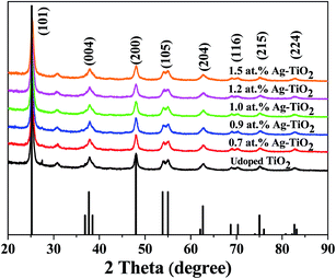 |
| | Fig. 1 XRD pattern of pure TiO2 and x at% Ag–TiO2. | |
Table 1 Ag contents in x at% Ag–TiO2 measured by XRF
| Samples (at% of Ag) |
Analyzed Ag content in at% |
| 0.7 |
0.45 |
| 0.9 |
0.63 |
| 1.0 |
0.84 |
| 1.2 |
1.03 |
| 1.5 |
1.21 |
The SEM morphology of different samples in Fig. 2 shows that the crystalline sizes for undoped TiO2 and at% Ag–TiO2 were in the region of 10–40 nm, which were in agreement with the size of nanoparticles determined from the diffraction peak of (101) and Scherer's equation and further confirms that the particle size were not noticeably influenced by the Ag-doping with the content ranging from 0.7 at% to 1.5 at%. Fig. 2 also shows that the obtained TiO2 and x at% Ag–TiO2 semiconductor materials consist of aggregated nanoparticles without any particular morphology.
 |
| | Fig. 2 SEM image of (a) undoped TiO2, (b) 0.7 at% Ag–TiO2, (c) 0.9 at% Ag–TiO2, (d) 1.0 at% Ag–TiO2, (e) 1.2 at% Ag–TiO2, (f) 1.5 at% Ag–TiO2. | |
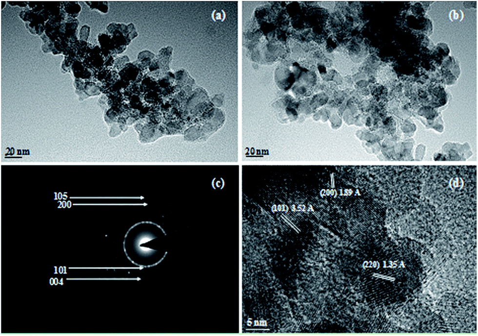
Further, a typical TEM image of undoped TiO2 and 1.2 at% Ag–TiO2 were also recorded and are shown in Fig. 3a and b, respectively. The TEM images further confirm that the crystalline sizes for undoped TiO2 and 1.2 at% Ag–TiO2 were in the region of 10–40 nm. Fig. 3c depicts the selected area electron diffraction (SAED) pattern of the 1.2 at% Ag–TiO2. The pattern clearly reveals bright concentric rings, which were due to the diffraction from the (101), (004), (200), and (105) planes of anatase TiO2. In the HRTEM image of 1.2 at% Ag–TiO2 (Fig. 3d), lattice fringes with d-spacing values of 3.52 Å, 1.89 Å, and 1.35 Å were observed, which corresponds to the (101), (200), and (220) planes of anatase TiO2.
 |
| | Fig. 3 TEM image of (a) undoped TiO2, (b) 1.2 at% Ag–TiO2, (c) SAED pattern and (d) HRTEM image of 1.2 at% Ag–TiO2. | |
X-ray photoelectron spectroscopy (XPS) was performed on the undoped and doped powders to compare the chemical state of the elements and explore how the doped silver cations interact with TiO2. The full scan XPS spectra of binding energy in Fig. 4a indicated that the material contained Ti, O, Ag elements together with trace contamination of C. In Fig. 4b, the peak position of the O 1s core levels of 1.0 at% Ag–TiO2 and 1.5 at% Ag–TiO2 shift to lower energy compared with those of undoped TiO2, indicating that the chemical environment of the elements has been changed.35,36 In x at% Ag–TiO2, some O–Ti was replaced by lower binding energy bind of O–Ag, therefore, the peak position of the O 1s core levels of x at% Ag–TiO2 shifts to lower energy, it is more obviously when the doping amount up to 1.5%. Similarly, two peaks of undoped-TiO2 at 457.9 and 463.6 eV, which were ascribed to Ti 2p3/2 and Ti 2p1/2, respectively, also shifted toward low binding energy (Fig. 4c). This phenomenon was attributed to the change of the local chemical environment of Ti ions influenced by Ag incorporation and the formation of Ag–O–Ti bonds on the surface of TiO2.37 For Ag 3d spectrum (Fig. 4d), two distinct peaks are observed at 367.9 and 373.9 eV. This doublet was assigned to Ag 3d5/2 and Ag 3d3/2 levels, respectively, coming from Ag+ ions. Although silver species was not observed in the XRD diagrams of x at% Ag–TiO2 even the concentration of Ag is up to 1.5% (as shown in Fig. 1), it is certain that some Ag ions have successfully substituted Ti ions in the TiO2 lattice during the solvothermal process, and some Ti–O bonds in TiO2 have been replaced by Ag–O bonds.
 |
| | Fig. 4 X-ray photoelectron spectroscopy of undoped-TiO2, 1.0 at% Ag–TiO2 and 1.5 at% Ag–TiO2. (a) Full scan XPS spectrum, (b) O 1s spectrum, (c) Ti 2p spectrum and (d) Ag 3d spectrum. | |
3.2. Band edge movement analysis of Ag–TiO2
As important electronic parameters in DSSCs, the message of band edge positions of photoanode material in DSSCs is extremely important because it could be used to estimate the driving force for electron injection. Fig. 5 shows the UV-vis absorption spectroscopy of different samples. In Fig. 5, a broad absorption peak attributed to the intrinsic band gap of TiO2 (≈3.2 eV) is observed in the region of 300–400 nm, which was associated with the electronic excitation of the valence band O 2p electron to the conduction band Ti 3d level. After doped with Ag, the band edge of this absorption shifts toward long wavelength, which indicates that the band gap is narrowed by doping with Ag. And it is more obvious with the increase doping amount of Ag. Also, the red shift of light adsorption indicated that the band gap energy (Eg) of Ag-doped TiO2 was reduced. This is because that Eg of semiconductor materials could be calculated using the following formula:| |
 | (1) |
where λ is the adsorption wavelength from UV-vis spectroscopy in nanometers. The narrowed band gap and reduced band gap energy are all good for absorbing sunlight and enhance its photovoltaic performance.38
 |
| | Fig. 5 UV-vis absorption spectra of undoped-TiO2 and x at% Ag–TiO2. | |
As analysis by optical spectra, the narrowed band gap and reduced band gap energy means band edge movement occurs in Ag-doped TiO2. However, the details and mechanism are still unknown by optical spectra analysis. Therefore, a steady-state spectroelectrochemical measurement was introduced to determine the conduction band edge position and the band edge movement in the semiconductor materials of x at% Ag–TiO2. Spectroelectrochemistry is a method used to ascertain the conduction band position in semiconductor materials. As supposed by Michael Grätzel, the absorbance at 780 nm is proportional to the density of electrons in the conduction band.39 Therefore, the method of spectroelectrochemistry could firstly determine the concentration of electrons in the conduction band by measuring the absorption of photons with band gap energy in the semiconducting film and then ascertain the conduction band position. The absorbance of undoped TiO2 and x at% Ag–TiO2 thin films deposited on an FTO substrate measured at 780 nm as a function of applied potential are shown in Fig. 6. As shown in Fig. 6, the absorbance of undoped TiO2 and x at% Ag–TiO2 thin films all follows a rule of exponential functions of applied potential and the absorption improved with the increase of the applied negative potential. More electrons are obtained in Ag-doped TiO2 films than that of undoped TiO2 film at the same applied potential (absolute value > 300 mV).
 |
| | Fig. 6 Optical absorbance at 780 nm of undoped TiO2 and x at% Ag–TiO2 photoelectrode films. | |
The onset of x at% Ag–TiO2 films are also smaller (absolute value) than that of undoped TiO2 film. The smaller onset means a lower Fermi level of the x at% Ag–TiO2, which indicates a positive shift of the electron quasi-Fermi level. Usually, the conduction band edge will shift simultaneously by an equal displacement of quasi-Fermi level relative to the I3−/I− Fermi level, therefore, the conduction band edge of x at% Ag–TiO2 also shifts toward the positive direction.40 This positive shift of conduction band edge is the main contribution to the increase of absorbance for x at% Ag–TiO2. Meanwhile, combined with optical spectra analysis, it is easy to found that the narrowed band gap of x at% Ag–TiO2 is also caused by its positive shift of conduction band edge. Herein, band edge movement of Ag-doped TiO2 is confirmed by spectroelectrochemical measurement, and this spectroelectrochemical measurement also confirms that the decreased bottom of conduction band of TiO2 after doping with Ag has narrowed the band gap of TiO2 and improved driving force of injected electron, resulting in increased TiO2 (e−) concentration in conduction band.
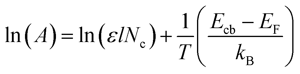
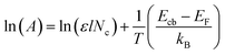
Furthermore, in order to quantitative analysis the effect of conduction band edge movement of TiO2 after doping with Ag on TiO2 (e−) concentration, another steady-state spectroelectrochemical measurement of 1.2 at% Ag–TiO2 with variable temperature was also applied. Fig. 7 shows the exponential distribution of the TiO2 (e−)s extracted from the variable temperature spectroelectrochemical data and are plotted as the chemical capacitance versus applied potential. In Fig. 7, the area below the exponential distribution curve stands for charge quantity in the conduction band of 1.2 at% Ag–TiO2 and undoped TiO2 at different temperature. It was obvious that the charge quantity in the conduction band of 1.2 at% Ag–TiO2 was larger than that of undoped TiO2 at any testing temperature. This is consistent with the results of spectroelectrochemical measurement above that Ag doping could reduce the bottom of conduction band of TiO2, increase TiO2 (e−) concentration and absorbance in conduction band. From Fig. 7 it could also be found that the charge quantity in the conduction band for both 1.2 at% Ag–TiO2 and undoped TiO2 increased with the raise of temperature, which could be easily interpreted by the relationship of TiO2 (e−) concentration and temperature as predicted by eqn (2).
| |
 | (2) |
where
kB is Boltzmann's constant,
T is test temperature,
Ecb is the energy of the conduction band edge,
EF is the Fermi level energy and
Nc is the states density of effective conduction band.
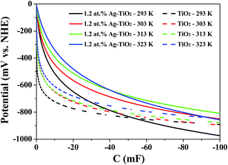 |
| | Fig. 7 Chemical capacitance for TiO2 and 1.2 at% Ag–TiO2 thin-film electrodes immersed in the standard electrolyte with 100 mM LiClO4, for TiO2 (e−) as a function of applied potential. | |
To obtain the quantity data of the band edge movement in 1.2 at% Ag–TiO2, the absorbance (A) for TiO2 and 1.2 at% Ag–TiO2 with different applied potential were plotted as a function of reciprocal temperature and shown in Fig. 8. The solid lines in Fig. 8 represent the results of a linear fit to eqn (3) for the data obtained at potentials between −0.45 and −0.70 V vs. Ag/AgCl.
| |
 | (3) |
 |
| | Fig. 8 Plot of ln(A) vs. T−1 each line represents a different potential from −0.45 to −0.70 V vs. Ag/AgCl in 50 mV increments from bottom to top. (a) Undoped TiO2 and (b) 1.2 at% Ag–TiO2. | |
As shown in Fig. 8, the absorbance increased with the increase of both temperature (moving from right to left of the plot) and applied potential (moving from down to up in the figure). From Fig. 8 and eqn (3), it can be conclude that the Ecb value of TiO2 and 1.2 at% Ag–TiO2 at different applied potentials could be calculated by the slope of lines in Fig. 8. Therefore, to get the Ecb value and further illustrate the band edge movement of Ag-doped TiO2, a global fit to all the data was performed to get the Ecb value at different applied potentials and the fit results are collected in Table 2. The fit results shown in Table 2 also indicate that the absolute values of Ecb increased as the increase of applied potential for both TiO2 and 1.2 at% Ag–TiO2. What's more, Ecb of 1.2 at% Ag–TiO2 is lower than that of undoped TiO2 at any applied potentials. This semi-quantitative analysis of variable temperature spectroelectrochemical measurement further confirms that conduction band edge of TiO2 shift positively after doping with Ag, which also verified the qualitative analysis results of conduction band edge movement by optical absorption and fixed temperature spectroelectrochemical measurement.
Table 2 Fit results of absorbance vs. temperature to eqn (3)
| EF (mV vs. Ag/AgCl) |
Ecb/q (mV vs. Ag/AgCl) |
| 1.2 at% Ag–TiO2 |
TiO2 |
| −450 |
−802.37 |
−790.31 |
| −500 |
−814.92 |
−823.73 |
| −550 |
−864.66 |
−856.89 |
| −600 |
−890.25 |
−882.62 |
| −650 |
−920.06 |
−910.77 |
| −700 |
−949.31 |
−940.85 |
3.3. Photovoltaic performance of DSSCs based on Ag–TiO2
In order to figure out the influence of Ag doping on the photoelectric properties of TiO2, different photoanodes based on TiO2 and x at% Ag–TiO2 were prepared and employed into N719 sensitized solar cells. The current–voltage (J–V) characteristic of the DSSCs devices based on different photoanodes under illumination (AM1.5G, 100 mW cm−2) are shown in Fig. 9, and the corresponding cells performance are summarized in Table 3. As shown in Fig. 9 and Table 3, the Voc decreases after doping with Ag at any amount levels. The Jsc increases when the TiO2 semiconductor doped with Ag, reaching a limit coinciding with an initial Ag quantity of 1.2 at%, after which the effect is reversed and the Jsc begins to fall. The decrease in efficiency at a high Ag loading (1.5 at%) was due to the free standing/excess Ag in the composite, which could oxidize to Ag(I) and erode to the redox electrolyte.41 The oxidation of the Ag would have acted as a new recombination center, thus reducing the number of charge carriers, which led to a decrease in the Jsc and Voc. Consequently, the overall conversion efficiency of the DSSC deteriorated. However, DSSC based on 1.2 at% Ag–TiO2 photoanode exhibited a Jsc of 19.75 mA cm−2, a Voc of 0.73 V, and a FF of 0.57 with the energy conversion efficiency (η) of 7.34%, indicating a 57% and 30% increase in Jsc and η respectively than the DSSC based on undoped TiO2 photoanode, which gives a Jsc of 12.61 mA cm−2, a Voc of 0.75 V, and a FF of 0.59 with a η of 5.64%.
 |
| | Fig. 9 Current density versus voltage curves of the DSSCs based on undoped TiO2 and x at% Ag–TiO2 photoanodes. | |
Table 3 Photoelectric properties and dye loading amount of different DSSCs
| Photoanodes |
Jsc (mA cm−2) |
Voc (V) |
FF |
η (%) |
Dye loading amount (10−7 mol cm−2) |
| Undoped-TiO2 |
12.61 |
0.75 |
0.59 |
5.64 |
1.21 |
| 0.7 at% Ag–TiO2 |
16.93 |
0.73 |
0.60 |
6.58 |
1.20 |
| 0.9 at% Ag–TiO2 |
17.54 |
0.74 |
0.60 |
6.90 |
1.21 |
| 1.0 at% Ag–TiO2 |
18.73 |
0.73 |
0.55 |
7.11 |
1.21 |
| 1.2 at% Ag–TiO2 |
19.75 |
0.73 |
0.57 |
7.34 |
1.20 |
| 1.5 at% Ag–TiO2 |
14.96 |
0.73 |
0.62 |
6.75 |
1.21 |
The decrease in the Voc is due to the conduction band edge movement of Ag–TiO2, as discussed above, the movement of conduction band edge potential (Ecb) of Ag-doped TiO2 decreases the energy gap between the Fermi level (EF) and the potential of the I−/I3− redox species (Ered) in the electrolyte, resulting in the phenomenon that the Voc of Ag-doped TiO2-based DSSC decreased. The Voc value can be described as eqn (4):
Assuming that Ered of I−/I3− in the electrolyte does not change with the dopant, it is anticipative that the Voc relies on the EF, which is related to the Ecb position. So it is definite that the lower conduction band edge of TiO2 results in less Voc.40
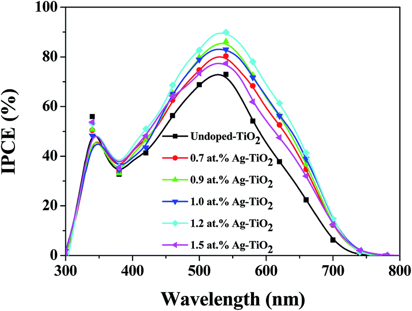
Although dye loading plays an important role in determine the photo-current density in DSSCs, the increase of Jsc in this study is not due the amount of dye adsorbed in the semiconductor films because the adsorption does not changed in the Ag-doped semiconductors, as shown in Table 3. Therefore, the increase of Jsc is due to several causes. First, as shown in Scheme 1, the conduction band edge moves to lower position after silver doping. This indicates the driving force for electron injection increases, which enhances the electron injection efficiency from the LUMO of the dye to the conduction band of TiO2. In addition, the inclusion of Ag nanoparticles resulted in a change in the Fermi energy level. The electrons in the conduction band of the TiO2 could be effectively captured by the Ag until a Fermi level equilibrium was obtained and the charge recombination process was minimized, which improved the DSSC performance. What's more, the increased Jsc is confirmed by IPCE response of cells, since they are related with the eqn (5):
| |
 | (5) |
where
e is the elementary charge and
ϕph.AM1.5G is the photon flux at AM1.5G, 100 mW cm
−2 irradiation.
42 Fig. 10 collected the IPCE spectra of different devices. As shown in
Fig. 10, upon doping TiO
2 with Ag, the IPCE spectrum of cells are enhanced in the region of 300–750 nm, which contributes to the increase of
Jsc.
 |
| | Scheme 1 Schematic on operation principles and photoinduced charge transfer process of DSSCs containing Ag–TiO2. | |
 |
| | Fig. 10 IPCE spectra of the DSSCs based on different photoelectrodes. | |
In order to illustrate the minimized charge recombination process in DSSCs based on Ag-doped TiO2, dark current measurement was firstly used to characterize the prepared DSSCs devices. Dark current measurement in DSSC can not be related directly to the back electron transfer process, since the electrolyte concentration in the films and the potential distribution across the nanoporous electrode in dark are different than those under illumination.43 However, a comparison of dark current between the investigated cells can provide useful information regarding the back electron transfer process. Therefore, dark current measurement of DSSCs has been considered as a qualitative technique to describe the extent of the back electron transfer.44 Fig. 11 shows the dark current–voltage characteristics of the DSSCs based on different photoelectrodes with the applied bias from 0 to +0.70 V. By comparing the curves in Fig. 11, it is found that when the concentration of Ag in the semiconductor is ≤1.2 at%, the dark current of the DSSCs based on x at% Ag–TiO2 increased much slower than that of DSSC based on undoped TiO2 when potential was greater than +0.25 V. In other words, under the same potential bias, when the potential was ≥0.25 V, the dark current for the DSSCs based on x at% Ag–TiO2 was noticeably smaller than that for the DSSC based on undoped TiO2. However, it is different when the concentration of Ag in the semiconductor is up to 1.5 at%, which indicates that a proper doping amount of silver in TiO2 semiconductor can successfully suppress the electron back reaction with oxide dye cation and/or the oxidized form of the redox shuttle, resulting in enhanced short circuit current density.
 |
| | Fig. 11 Dark current of the DSSCs based on different photoelectrodes. | |
EIS analysis was also used to study the interfacial charge transfer process in DSSCs based on undoped-TiO2 and x at% Ag–TiO2, respectively. The measurements were scanned from 0.1 to 100 kHz at room temperature with an applied bias voltage of 0.75 V. The Nyquist plots for the devices under dark condition are shown in Fig. 12a. The diameters of the medium-frequency semicircle increased when the concentration of Ag in the semiconductor is ≤1.2 at%, implying that the recombination reaction between the conduction band electrons in TiO2 film and electrolyte is better inhibited by doping with silver.45 While, when the concentration of Ag in the semiconductor exceeds 1.2 at%, the diameters of this semicircle decreased is also due to the oxidation of the Ag caused by excessive silver, which accelerate the recombination of injected electrons. This is consistent with the result of dark current measurement. The Nyquist plots for the devices under standard AM1.5G solar irradiation are shown in Fig. 12b. The large medium-frequency semicircles are assigned to the charge transfer processes at TiO2/dye/electrolyte interface, whose radius are decreased after doping with ≤1.2 at% Ag, suggesting a decrease of the electron transfer impedance at this interface. However, when the doping amount exceeds 1.2 at%, the electron transfer impedance at this interface increased due to the formation of more recombination centers in the semiconductor. The increase of charge recombination impedance and the decrease of electron transfer impedance in DSSCs are all benefit for performance improving.
 |
| | Fig. 12 Nyquist plots of DSSCs based on different photoelectrodes measured (a) in dark, (b) under standard AM1.5G solar irradiation. | |
Furthermore, the OCVD technique has been employed as a powerful tool to study interfacial recombination processes in the TiO2 DSSCs between photo-injected electrons and the electrolyte in the dark.46,47 It can provide some quantitative information on the electron recombination rate. Fig. 13 shows the OCVD decay curves of the DSSCs based on different photoelectrodes. It was observed that the OCVD response of the DSSCs with x at% Ag–TiO2 (x ≤ 1.2) photoelectrode were much slower than that with undoped-TiO2 photoelectrode, especially in the shorter time domain (within 30 s). Since the decay of the Voc reflects the decrease in the electron concentration, which is mainly caused by the charge recombination,48 the cell with x at% Ag–TiO2 (x ≤ 1.2) photoelectrode has a lower electron recombination rate than that of the cell with undoped-TiO2 photoelectrode. This further confirmed the results of EIS analysis in dark conditions.
 |
| | Fig. 13 Open-circuit voltage decay curves of the DSSCs based on different photoelectrodes. | |
4. Conclusions
Ag-doped TiO2 was prepared by an easy hydrothermal route and employed into ruthenium dye N719 sensitized solar cells. It was found that the Ag is incorporated into the structure of the TiO2. After doping with Ag, the conduction band edge moves to lower position. This positive shift of conduction band edge implies a decrease in the open-circuit voltage of DSSCs. However, lower movement of conduction band edge provides stronger driving force for electrons injection from the LUMO of the dye to the conduction band of TiO2. The deposition of Ag not only benefits for efficient charge transfer but also could effectively suppress the charge recombination between injected electrons and oxide dye cation and/or the oxidized form of the redox shuttle, resulting in a significant photocurrent enhancement. The DSSC based on 1.2 at% Ag–TiO2 photoanode exhibited a Jsc of 19.75 mA cm−2, a Voc of 0.73 V, and a FF of 0.57 with the energy conversion efficiency (η) of 7.34%, indicating a 57% and 30% increase in Jsc and η respectively than that of DSSC based on undoped TiO2 photoanode.
Acknowledgements
This work was supported by National Natural Science Foundation of China (Grant 21571042, 21171044 and 21371040) and the National key Basic Research Program of China (973 Program, 2013CB632900).
References
- B. O'Regan and M. Grätzel, Nature, 1991, 353, 737–740 CrossRef.
- M. Grätzel, Acc. Chem. Res., 2009, 42, 1788–1798 CrossRef PubMed.
- S. K. Balasingam, M. Lee, M. G. Kang and Y. Jun, Chem. Commun., 2013, 49, 1417–1487 Search PubMed.
- P. P. Das, S. Mukhopadhyay, S. A. Agarkar, A. Jana and P. S. Devi, Solid State Sci., 2015, 48, 237–243 CrossRef CAS.
- C. K. Dong, W. C. Xiang, F. Z. Huang, D. C. Fu, W. C. Huang, U. Bach, Y. B. Cheng, X. Li and L. Spiccia, Nanoscale, 2014, 6, 3704–3711 RSC.
- E. L. Unger, S. J. Fretz, B. Lim, G. Y. Margulis, M. D. McGehee and T. D. P. Stack, Phys. Chem. Chem. Phys., 2015, 17, 6565–6571 RSC.
- L. Tu, H. Pan, H. Xie, A. Yu, M. Xu, Q. Chai, Y. Cui and X. Zhou, Solid State Sci., 2012, 14, 616–621 CrossRef CAS.
- T. Chen, S. Wang, Z. Yang, Q. Feng, X. Sun, L. Li, Z. S. Wang and H. Peng, Angew. Chem., Int. Ed., 2011, 50, 1815–1819 CrossRef CAS PubMed.
- Z. S. Wang, Y. Cui, Y. Dan-oh, C. Kasada, A. Shinpo and K. Hara, J. Phys. Chem. C, 2008, 112, 17011–17017 CAS.
- K. H. Ko, Y. C. Lee and Y. J. Jung, J. Colloid Interface Sci., 2005, 283, 482–487 CrossRef CAS PubMed.
- Y. D. Duan, J. Zheng, M. Xu, X. Song, N. Fu, Y. Fang, X. Zhou, Y. Lin and F. Pan, J. Mater. Chem. A, 2015, 3, 5692–5700 CAS.
- S. K. M. Saad, A. A. Umar, M. Y. A. Rahman and M. M. Salleh, Appl. Surf. Sci., 2015, 353, 835–842 CrossRef CAS.
- S. Lee, J. H. Noh, H. S. Han, D. K. Yim, D. H. Kim, J. K. Lee, J. Y. Kim, H. S. Jung and K. S. Hong, J. Phys. Chem. C, 2009, 113, 6878–6882 CAS.
- X. Lü, X. Mou, J. Wu, D. Zhang, L. Zhang, F. Huang, F. Xu and S. Huang, Adv. Funct. Mater., 2010, 20, 509–515 CrossRef.
- B. Zhao, J. Wang, H. Li, H. Wang, X. Jia and P. Su, Phys. Chem. Chem. Phys., 2015, 17, 14836–14842 RSC.
- A. M. Bakhshayesh and N. Bakhshayesh, J. Colloid Interface Sci., 2015, 460, 18–28 CrossRef CAS PubMed.
- H. Tian, L. Hu, C. Zhang, W. Liu, Y. Huang, L. Mo, L. Guo, J. Sheng and S. Dai, J. Phys. Chem. C, 2010, 114, 1627–1632 CAS.
- A. Malik, S. Hameed, M. J. Siddiqui, M. M. Haque, K. Umar, A. Khan and M. Muneer, J. Mater. Eng. Perform., 2014, 23, 3184–3192 CrossRef CAS.
- K. P. Wang and H. Teng, Phys. Chem. Chem. Phys., 2009, 11, 9489–9496 RSC.
- W. W. Xu, S. Y. Dai, L. H. Hu, L. Y. Liang and K. J. Wang, Chin. Phys. Lett., 2006, 23, 2288–2291 CrossRef CAS.
- J. T. Park, W. S. Chi, H. Jeon and J. H. Kim, Nanoscale, 2014, 6, 2718–2729 RSC.
- Z. Liu, Y. Li, C. Liu, J. Ya, L. E. W. Zhao, D. Zhao and L. An, ACS Appl. Mater. Interfaces, 2011, 3, 1721–1725 CAS.
- A. R. Tanyi, A. I. Rafieh, P. Ekaneyaka, A. L. Tan, D. J. Young, Z. Zheng, C. Vijila, G. S. Subramanian and R. L. N. Chandrakanthi, Electrochim. Acta, 2015, 178, 240–248 CrossRef CAS.
- D. H. Kim, G. S. Han, W. M. Seong, J. W. Lee, B. J. Kim, N. G. Park, K. S. Hong, S. Lee and H. S. Jung, ChemSusChem, 2015, 8, 2392–2398 CrossRef CAS PubMed.
- M. Yang, R. Guo, K. Kadel, Y. Liu, K. O'Shea, R. Bone, X. Wang, J. He and W. Li, J. Mater. Chem. A, 2014, 2, 19616–19622 CAS.
- J. J. Mock, M. Barbic, D. R. Smith, D. A. Schullz and S. J. Schullz, J. Chem. Phys., 2002, 116, 6755–6759 CrossRef CAS.
- C. Wen, K. Ishikawa, M. Kishima and K. Yamada, Sol. Energy Mater. Sol. Cells, 2000, 61, 339–351 CrossRef CAS.
- Y. Gao, P. Fang, F. Chen, Y. Liu, Z. Liu, D. Wang and Y. Dai, Appl. Surf. Sci., 2013, 265, 796–801 CrossRef CAS.
- K. C. Lee, S. J. Lin, C. H. Lin, C. S. Tsai and Y. J. Lu, Surf. Coat. Technol., 2008, 202, 5339–5342 CrossRef CAS.
- S. P. Lim, A. Pandikumar, H. N. Lim, R. Ramaraj and N. M. Huang, Sci. Rep., 2015, 5, 11922 CrossRef PubMed.
- S. H. Hwang, H. Song, J. Lee and J. Jang, Chem.–Eur. J., 2014, 20, 12974–12981 CrossRef CAS PubMed.
- P. Y. Reddy, L. Giribabu, C. Lyness, H. J. Snaith, C. Vijaykumar, M. Chandrasekharam, M. Lakshmikantam, J. H. Yum, K. Kalyanasundaram, M. Grätzel and M. K. Nazeeruddin, Angew. Chem., Int. Ed., 2007, 46, 373–376 CrossRef CAS PubMed.
- N. G. Park, J. van de Lagemaat and A. J. Frank, J. Phys. Chem. B, 2000, 104, 8989–8994 CrossRef CAS.
- J. T. Tang, X. M. Chen, Y. Liu, W. Gong, Z. S. Peng, T. J. Cai, L. J. Luo and Q. Deng, Solid State Sci., 2013, 15, 129–136 CrossRef CAS.
- B. Xin, L. Jing, Z. Ren, B. Wang and H. Fu, J. Phys. Chem. B, 2005, 109, 2805–2809 CrossRef CAS PubMed.
- X. Chen, L. Song, L. You and L. Zhao, Appl. Surf. Sci., 2013, 271, 248–252 CrossRef CAS.
- Y. C. Cao, Z. Y. Zhao, J. Yi, C. S. Ma, D. C. Zhou, R. F. Wang, C. Li and J. B. Qiu, J. Alloys Compd., 2013, 554, 12–20 CrossRef CAS.
- M. Saif and M. S. A. Abdel-Mottaleb, Inorg. Chim. Acta, 2007, 360, 2863–2874 CrossRef CAS.
- G. Rothenberger, D. Fitzmaurice and M. Grätzel, J. Phys. Chem., 1992, 96, 5983–5986 CrossRef CAS.
- J. Yu, Y. L. Yang, R. Q. Fan, L. Li and X. Y. Li, J. Phys. Chem. C, 2014, 118, 8795–8802 CAS.
- G. Zhao, H. Kozuka and T. Yoko, Sol. Energy Mater. Sol. Cells, 1997, 46, 219–231 CrossRef CAS.
- A. Hagfeldt, G. Boschloo, L. C. Sun, L. Kloo and H. Pettersson, Chem. Rev., 2010, 110, 6595–6663 CrossRef CAS PubMed.
- A. Zaban, A. Meier and B. A. Gregg, J. Phys. Chem. B, 1997, 101, 7985–7990 CrossRef CAS.
- S. Ito, P. Liska, P. Comte, R. Charvet, P. Pechy, U. Bach, L. Schmidt-Mende, S. M. Zakeeruddin, A. Kay, M. K. Nazeeruddin and M. Graetzel, Chem. Commun., 2005, 25, 4351–4353 RSC.
- W. Zhang, R. Zhu, X. Liu, B. Liu and S. Ramakrishna, Appl. Phys. Lett., 2009, 95, 043304 CrossRef.
- J. Bisquert, A. Zaban, M. Greenshtein and I. Mora-Sero, J. Am. Chem. Soc., 2004, 126, 13550–13559 CrossRef CAS PubMed.
- K. Fan, W. Zhang, T. Y. Peng, J. N. Chen and F. Yang, J. Phys. Chem. C, 2011, 115, 17213–17219 CAS.
- H. Yua, S. Q. Zhang, H. J. Zhao, G. Willb and P. Liu, Electrochim. Acta, 2009, 54, 1319–1324 CrossRef.
|
| This journal is © The Royal Society of Chemistry 2016 |
Click here to see how this site uses Cookies. View our privacy policy here.