Ping-Yen Hsieh,
Duc-Dung Nguyen,
Chi-Young Lee and
Nyan-Hwa Tai*
Department of Materials Science and Engineering, National Tsing Hua University, No. 101, Section 2, Kuang-Fu Road, Hsinchu 30013, Taiwan, Republic of China. E-mail: nhtai@mx.nthu.edu.tw; Fax: +886 3 5737406; Tel: +866 3 5715131 ext. 42568
First published on 28th July 2016
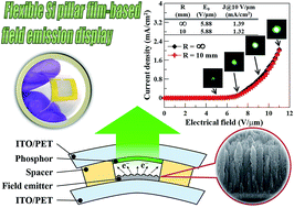
We report a new approach for the synthesis of various crystalline Si nanostructures on a polyimide (PI) substrate via microwave plasma enhanced chemical vapor deposition (MWPECVD) using SiCl4/H2 as precursors, and study the effects of conducting type (i.e., intrinsic, n-type, and p-type) on the electron field emission (EFE) properties of the Si nanostructures. H2 plasma treated B-doped crystalline Si pillars (H2: p-Si pillars) with a diameter of 50 nm and a sharp tip radius of 16 nm on a Mo-coated PI substrate reveals the best EFE performance with a low turn-on field of 5.85 V μm−1, high current density of 1.37 mA cm−2@10 V μm−1, and an extremely high field enhancement factor of 1281.13. This superior EFE performance is achieved because of its geometric features and high conductivity across the emitters. In addition, a flexible crystalline Si film-based field emission prototype device using the H2: p-Si pillar sample as the cathode is constructed. No obvious deterioration on EFE characteristics is observed when the device is subjected to bending at a radius of curvature (R) of 10 mm. According to the lifetime test, we achieve a half-life time over 10 h when a repeating FE-on/off test of 9 times at an R of 10 mm is performed, indicating high flexibility and good stability. These results thus demonstrate important steps toward a low-cost approach for creating high-performance and flexible field emission displays.
From another perspective, developing Si-based field emitters is highly desirable because of the widely utilized Si material and process compatibility with the already existing Si integrated circuit technology.10 Unfortunately, the EFE characteristics of Si-based materials are still unsatisfactory. Intensive research efforts have been devoted to improving the EFE properties of Si materials. Besides the requirement of high-quality crystallinity for obtaining high carrier mobility, these modification techniques include nanostructure engineering,10–14 H2 plasma treatment,13,14 metal implantation,15 adoption of a metal interfacial layer16 and coverage with metal particles,11 carbon nanomaterial film,12 and ferroelectric film.17 Among the abovementioned methods, two primary strategies, formation of nanostructure with small apex radius and increasing the conductivity, are employed to achieve superior EFE performance. The former involves sharp features, which increase the localized electric field owing to geometric features of the emitter. This leads to facile emission of electrons from the Si surface at low E0 and a drastic increase in the field enhancement factor (β) in comparison with its flat surface counterpart.18,19 On the other hand, incorporation of dopant or metal in the Si structure renders the Si-based material even more conductive and is thus a route for enhancing electron transport. It results in the EFE devices with low E0 accompanied by high J.11,15 Owing to the aforementioned modification techniques, Si-based EFE devises exhibiting high emission current and ballasting effect by using nanostructured Si arrays as emitters were developed to date.20,21 Such nanostructured Si arrays were fabricated from high-quality crystalline Si wafer using top-down etching process. However, to the best of our knowledge, the integration of Si film-based field emitters into flexible device architectures has not been reported. This is most likely due to poor thermal stability of polymer substrates and an immature transfer process.
Our previous study reported the feasibility of using microwave plasma enhanced chemical vapor deposition (MWPECVD) with a SiCl4/H2 mixture to directly deposit highly crystalline Si film onto polyimide (PI) substrate at a temperature as low as 185 °C.22 Furthermore, a self-biased sputtering solid doping source (SSSDS) process incorporated with SiCl4/H2 microwave plasma was adopted to effectively dope dopant atoms into the Si network for growing doped crystalline Si films.23 In order to continue our efforts on the development of MWPECVD grown Si nanostructures on polymer substrates toward flexible electronics, we herein present a new strategy to fabricate Si pillars using ultrathin Au film as a catalyst to induce the vapor–solid–solid (VSS) reaction in the aforementioned Si deposition system and thus to grow doped crystalline Si pillars. The VSS mechanism using Au catalyst appears to be the favorable process for the synthesis of Si nanostructure because the growth temperature can be lower than the eutectic temperature of the Au–Si system (∼363 °C). It leads to less unintentional incorporation of impurities, resulting from the reduction in atom diffusivity and solid solubility associated with the lower temperatures.24 The doped crystalline Si pillars was further treated by the H2 plasma dry etching process to generate a sharp nanostructure with a small apex radius at the pillar tips. This step makes the specific nanoscale structures ideal field emitters. In addition, a sputtered Mo interfacial layer was introduced between the crystalline Si film and PI substrate, where the Mo metal film can increase the lateral conductivity and enhance electron transport. The present study focused on the effects of the conducting type (i.e., intrinsic, n-type, and p-type) and nanostructure morphology on the EFE property of the synthesized crystalline Si film. Moreover, a flexible Si film-based EFE (Si-EFE) prototype device was fabricated by using H2 plasma treated B-doped crystalline Si pillars on Mo-coated PI substrate as the cathode. Their EFE characteristics, lifetime stability, and bending durability were evaluated in detail.
The electrical conductivity (σ) of the synthesized crystalline Si film samples was measured by an electrometer (Keithley 2400) using a sputtered Al film (∼100 nm) as ohmic contact between Si film and electrode. To investigate the effect of structural characteristics on the transport behavior of electrons, two configurations were utilized: (i) a pair of electrodes located on the surface of the crystalline Si film for measuring the conductivity along the Si film surface (designated as σ∥) and (ii) a setup with one electrode located on the crystalline Si film surface and the other located on the Mo interfacial layer for measuring the conductivity across the crystalline Si film thickness (designated as σ⊥).
The EFE property of the synthesized crystalline Si films was measured by using a tunable parallel-plate capacitor setup, in which a Mo hemispherical probe with 2 mm diameter was used as anode and crystalline Si film samples were used as cathode. The cathode-to-anode distance was controlled by using a micrometer. The current–voltage characteristics were acquired under high vacuum at a pressure below 1 × 10⁻⁶ Torr by using an electrometer (Keithley 2410). On the basis of the Fowler–Nordheim (F–N) theory,25 the EFE characteristics were modeled as shown in eqn (1),
![]() | (1) |
![]() | ||
Fig. 1 Photograph and schematic cross-sectional image of the fabricated flexible crystalline Si-EFE prototype device. |
The EFE characteristics of the crystalline Si-EFE prototype device were measured by using an electrometer (Keithley 2410) under high vacuum with a pressure below 1 × 10⁻⁶ Torr. In addition, the flexibility was evaluated by mechanical static bending tests, in which the flexible Si-FED was bent to generate a tensile strain at a designated radius of curvature (R) of 10 mm. Moreover, lifetime measurement was also performed to evaluate the stability and durability of the crystalline Si-EFE prototype device by repeating FE-on and FF-off pulses separated by a duration of 1 h under a bended state. The current density–time (J–t) behavior was recorded during the test.
Detailed observation of XRD patterns in Fig. 2(a) shows that a slight decrease in intensity and slight broadening of the full width at half maximum were observed in the diffraction peaks of the four doped crystalline Si film samples, i.e., n-Si film, p-Si film, p-Si pillars, and H2: p-Si pillars, as compared with that of i-Si film. This finding implies the decreases of crystallinity and crystal size after introduction of the dopants into the Si films.
Similar tendencies of crystallization characteristics may also be seen in the Raman spectra shown in Fig. 2(b). Raman spectrum of the i-Si film reveals a sharp peak centered at 520.4 cm−1 and a high XC value of 98.5%. By comparison, the doped crystalline Si films, regardless of their structure, exhibited a dominant peak close to 517–518 cm−1 and a weak peak around 480 cm−1. The XC in these doped crystalline Si film samples are over 90% even they contained a small amount of amorphous Si phases. The results shown in the Raman spectra also confirm that both XC and crystallite size decreased upon doping the crystalline Si film with the impurity. These results agree with amorphization of the doped Si network with local deformation caused by dopant atoms.27 However, it is interesting to note that XC in the H2: p-Si pillars was improved after treatment of the p-Si pillars with H2 plasma. This improvement is most likely due to removal of the amorphous phase, disordered structure, and native oxide through the in situ H2 plasma etching process.14,28
Cross-sectional morphologies of crystalline Si films having different structures are illustrated in Fig. 3. A remarkable dense columnar morphologies are found in i-Si film, n-Si film, and p-Si film samples, which agree very well with the findings of high-crystallinity characteristics from XRD and Raman analyses (Fig. 2). The high growth rate of these films under microwave glow discharge decomposition of a SiCl4/H2 mixture could also be observed in Fig. 3(a)–(c). After deposition for 3 min, the i-Si, n-Si, and p-Si films reached thicknesses of 739, 794, and 786 nm, respectively. These thicknesses are substantially higher than those obtained from many other PECVD systems using SiH4/H2 or SiH2Cl2/H2 mixtures as precursors with or without gaseous doping.29–31 The enhancement in growth rate of the doped crystalline Si films may be due to the incorporation of dopants in the Si films. After the VSS reaction using an ultrathin Au film as catalyst in SiCl4/H2 microwave plasma with the SSSDS process, the morphology markedly changed from a continuous columnar morphology to a featured isolated columnar morphology, as shown in Fig. 3(d). In our case, the crystalline p-Si pillars exhibited grains with 785 nm length, approximate 50 nm diameter, and 20 nm separation (Fig. 3(d)); therefore, the density of the Si-pillars is around 109 # per cm2. After the growth of the crystalline p-Si pillars, the nanostructured morphology was subsequently modified by a H2 plasma process where the B-doped crystalline Si pillars was physically sputtered off, particularly the amorphous phase, native oxide, and edge-side structure. Consequently, a geometrically sharp nanostructure with a small apex radius around 16 nm formed at the tip. In addition, based on the statistic calculation, most of the diameter and the tip curvature of the H2 plasma treated Si pillars are in the range of 50–65 nm and 14–17 nm, respectively, as shown in Fig. S3.† This indicates a well control of the Si nanostructure by using the VSS mechanism in SiCl4/H2 microwave plasma as proposed in this study. Morphological evidence can be found in Fig. 3(e) and (f).
To better understand the microstructure of the H2 plasma treated B-doped crystalline Si pillar structure, TEM studies were carried out. The left micrograph in Fig. 4(a) shows a cross-sectional BFI of the H2: p-Si pillar sample, and the right-hand side displays its SAED pattern. HRTEM images captured at positions labeled with squares (I) and (II), corresponding respectively to the interface and the top regions of the synthesized H2: p-Si pillars, are shown beside the BFI image in Fig. 4(b) and (c), respectively. FFT patterns at positions (i) to (iii) in Fig. 4(b) and (iv) in Fig. 4(c) are also presented. The cross-sectional BFI reveals a completely crystalline pillar structure with grain sizes of around 50 nm throughout the thickness. The SAED pattern consists of distinct spots without a broad diffuse ring, indicating a well-defined polycrystalline Si structure with a large grain size; in addition, signals for the Au and Mo interlayer can also be seen in the SAED pattern. HRTEM microstructure of the synthesized H2: p-Si pillar sample at the interface between the Au catalyst and Si pillar structure (region (I) of Fig. 4(a) and also Fig. 4(b)) revealed a ultrathin Au-silicide layer with a depth of around 3 nm on the Au catalyst surface and a lattice spacing of approximately 0.26 nm (image (i)). These can be indexed to the (660) planes of the Au2Si phase.11 Subsequently, crystalline Si with (111) plane, confirmed from the lattice spacing (image (ii)), was originated vertically from the top surface of the Au-catalyst and then preceded the development of an almost entirely crystalline Si pillar structure containing predominantly (111) and (220) planes (image (iii)). Elemental composition analysis of the interface between the Au catalyst and Si pillar structure are also validated by EDS line-scan elemental profiles as shown in Fig. 4(d). No amorphous incubation layer surrounding the Au catalyst and no residual contamination from the Au in the Si pillar structure were found after careful HRTEM examinations. These results suggest that the as-grown crystalline Si pillars follows the VSS growth mechanism under the base growth scheme.
One important point to emphasize is the formation of sharp features at the topmost layer consisting of well-defined Si(111) planes in region (II) of Fig. 4(a), as shown in Fig. 4(c). According to our previous study on the growth mechanisms of crystalline Si films using SiCl4/H2 as reactants,22 the stronger etching ability of H and Cl radicals on the Si network facilitate the crystallization of the Si film at low temperatures through the effects of surface etching, self-cleaning, and chemical annealing. The anisotropic etching rate of Si depends on the surface crystal orientation in the order (100) ≥ (110) ≫ (111). Therefore, the chemical stability of the (111) grain is much higher than that of other grains which are thus preferentially etched away. As a result, retention of the Si(111) grain in the Si film with nearly single crystalline Si(111) at the topmost layer is expected. Therefore, the Si pillars growth presented in this study also meets such a criterion. Upon close inspection of HRTEM images, we observed no deterioration of crystal structure at the top region of the pillar structure even when it was subjected to H2 plasma dry etching.
It is known that the formation of metal silicide at the initial reaction is the key point in the Si-based VSS growth mechanism.32 Up to now, growth of Si nanostructures through VSS mechanism using Al,33 Au24 and Cu32 as catalyst at temperature of 430 °C, 350 °C and 510 °C, respectively had been reported. These synthesis temperature are below their eutectic temperature. In addition, the requirement of thermal energy is strongly depended on the decomposition of Si-based precursor and then facilitate the metal-silicide formation.24 In this study, the growth temperature of crystalline Si film of 185 °C for a deposition time of 3 min were estimated by using an infrared pyrometer aiming at the substrate holder. It is of interest how Au film could interact with Si to form a Si pillar structure in SiCl4/H2 microwave plasma at such low temperature. Plasma dry etching of Au film using F- or Cl-containing reactants, e.g., CF4–CCl4 mixtures34 and pure Cl2,35 is a well-known technique. Fortunately, the etching species H, Cl and SiClx (1 ≤ x ≤ 3) radicals existed in microwave plasma when SiCl4 and H2 were used as the reactants. We believe that the Cl-based radicals had etching ability upon reaching the Au surface, and thus formed the catalyst with nanosized Au particles from the initial Au film. Additionally, MWPECVD exhibiting high-density plasma and high ionization rate22,23 allows a further decrease in synthesis temperature by using plasma activation. Because of these two reasons, developing a crystalline Si pillar structure even under a low substrate temperature (lower than 185 °C) became possible. This was achieved by formation of nanosized Au-catalyst particles using plasma dry etching of Cl-based radicals followed by preferential growth of Si nanostructures from Au-catalyst particles via VSS mechanism through a metal-silicide (Au2Si) formation in SiCl4/H2 microwave plasma. According to the abovementioned results, the suggested growth mechanism of the crystalline Si pillars synthesized using SiCl4/H2 microwave plasma via Au-catalyzed VSS mechanism is proposed in Fig. 5.
Electron transport is known to proceed from the bottom to the top of the films during EFE behavior. Consequently, evaluation of electron transport ability across the Si film (i.e., σ⊥) is important, as it significantly affects EFE performance. According to the results shown in Fig. 6, the σ⊥ values of all crystalline Si film samples are higher than σ∥. A probable explanation for these results is the microstructure feature, viz., columnar structure for i-Si, n-Si, and p-Si films, as well as pillar structure for p-Si and H2: p-Si pillars. Such structures feature an electrical transport path along the length of the columnar grains, which are perpendicular to the substrate and thus bypass the clustered defects and grain boundaries between the columns. Therefore, a high performance in EFE characteristics was anticipated.
As expected, the negligible EFE characteristics of the i-Si film with an E0 of 23.22 V μm−1 (here, defined as the E needed to extract a J of 10 μA cm−2) and a low J of 2.86 × 10⁻⁴ mA cm−2 at an applied E of 10 V μm−1 were obtained. The high applied E and extremely low J value indicate that emission of electrons from the i-Si film surface is difficult. In contrast, the n-Si film could be switched on at an E0 of 11.93 V μm−1 to attain a J value of 4.64 × 10⁻³ mA cm−2@10 V μm−1; whereas p-Si film needed a lower E0 (10.31 V μm−1) to turn on the EFE behavior and achieve a higher EFE capacity (J = 9.34 × 10⁻³ mA cm−2@10 V μm−1). β, which is a parameter dependent on the geometry, electron transport ability, crystal structure, and density of emitter of the emission sites, may be estimated from the F–N equation to assess the degree of EFE characteristics of the materials.36 The β value can be derived from eqn (1) and expressed as follows (eqn (2)):
![]() | (2) |
In addition, the EFE performance from p-Si film occurring at a lower E and a higher J were also found. The p-Si and the n-Si films with substantial similarities in microstructure characteristics and σ suggest that localized field enhancement and ability for electron transport play insignificant roles in this situation. According to the literature, the difference in EFE performance is ascribed to band bending induced by surface states.18,19,36 For the n-type cathode, mid-band-gap surface states become negatively charged, resulting in the formation of a potential barrier. This potential barrier prevents electrons from reaching the apex of the n-type cathode. As band-bending acts opposite in a p-type cathode, there exists no surface potential barrier for the electrons (the minority carriers) transport to the emission site.18,19,36 This is the reason why the p-Si film exhibited better EFE characteristics than the n-Si film.
The effect of nanostructures on EFE performance was also investigated. The p-Si pillar sample possessed superior EFE properties, viz., the EFE process could be turned on at E0 of 7.97 V μm−1 with a J of 5.10 × 10⁻¹ mA cm−2@10 V μm−1, in contrast to the p-Si film. The corresponding β is as high as 940.92. Furthermore, E0 further decreased to 5.85 V μm−1, with J sharply increasing to 1.37 mA cm−2@10 V μm−1 after the H2 plasma dry etching process. Hence, the H2: p-Si pillar sample exhibited an outstanding β value of 1281.13, which is almost four times higher than that of the i-Si film. EFE characteristics are well understood to be a result of combined effects of both electrical and geometric contributions. Because of similar results of σ for the p-Si film, p-Si pillar, and H2: p-Si pillar samples (Fig. 6), the main factor leading to enhancement of EFE performance for the latter two these samples is ascribed to the formation of nanostructures. Nanostructures with sharp configuration features and nanosized diameter increase the localized electric field, leading to facile emission of electrons from the surface of the material.18,19 Therefore, the H2: p-Si pillar sample with high σ and consisting of a B-doped crystalline Si pillar structure with 50 nm diameter and a sharp feature with a small apex radius at its tip is a promising material for an ideal field emitter. An additional benefit for higher EFE performance is resulting from the reduction of the barrier layer due to removal of the native oxide surrounding the as-synthesized p-Si pillar structure via H2 plasma treatment.14
As compared with the published data on EFE characteristics of nanostructured Si films (Fig. 8) prepared on heterogeneous substrate using various bottom-up approaches,10,14,16,37–40 this study demonstrate that H2 plasma treated B-doped crystalline Si pillar sample possessed high EFE performance with E0 = 5.85 V μm−1, J = 1.37 mA cm−2@10 V μm−1, and β = 1281.13.
![]() | ||
Fig. 8 Comparison of EFE performance of nanostructured Si film samples prepared on a heterogeneous substrate by using various bottom-up approaches. |
Lifetime measurements of the flexible Si-EFE prototype device were carried out because the stability and durability is an important parameter related to prospective applications of the field emitters. During the measurement, the Si-EFE prototype device was bent under an R value of 10 mm, and then a constant voltage of 900 V (i.e., E of 9 V μm−1) with a pulse width of 1 h was applied to generate periodical FE-on/FE-off tests for simulating practical operations. The results obtained are plotted as J–t curves (Fig. 10). The J@9 V μm−1 of the bent Si-EFE prototype device remained stable over a period of 13 h which consists of a FE-on time of 7 h and FE-off of 6 h. After the lifetime measurement was extended to 19 h, the J@9 V μm−1 still retain near 58% of its initial current, indicating a half-life time (τEFE) of over 10 h. The decrease in J is believed to be due to the formation of an oxide layer from the adsorption of oxygen under a vacuum environment with a pressure below 1 × 10⁻⁶ Torr, which results in an increase in the potential barrier for electron tunneling.37 Therefore, the synthesized sample possessing very high stability, as compared with that made of carbon nanomaterials or other Si-based materials, demonstrates the feasibility of application in flexible devices.
In summary, a flexible Si-EFE prototype device based on H2 plasma treated B-doped crystalline Si pillars on Mo/PI substrate as field emitter was reported. To synthesize the Si pillar nanostructure, we carried out microwave glow discharge decomposition of H2–diluted SiCl4 mixture incorporate with the SSSDS process using Au-catalyzed VSS mechanism followed by H2 plasma dry etching process. The H2: p-Si pillar sample exhibited high EFE performance with E0 = 5.85 V μm−1, J = 1.37 mA cm−2@10 V μm−1, and β = 1281.13. Furthermore, the high flexibility and stability of the Si-EFE prototype device was also demonstrated. According to the results, it is suggested that the flexible H2: p-Si pillars may hold promise for the development of a next-generation cathode material for high-performance EFE devices. Linking the flexible crystalline Si-thin film transistor22 acted as active-matrix driver electronics, a flat panel display integrated with fully Si material on a flexible polymer substrate can now be envisaged.
Footnote |
† Electronic supplementary information (ESI) available. See DOI: 10.1039/c6ra10255g |
This journal is © The Royal Society of Chemistry 2016 |