DOI:
10.1039/C6RA10132A
(Paper)
RSC Adv., 2016,
6, 75839-75843
Sensor based on chemical vapour deposition-grown molybdenum disulphide for gas sensing application
Received
19th April 2016
, Accepted 30th July 2016
First published on 1st August 2016
Abstract
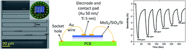
Over the past few decades, sensors based on field-effect transistors have drawn much attention. Initially three dimensional materials were used for sensing, which were later replaced by two dimensional materials because of their ease of manufacturing and large specific areas. Amongst the transition metal dichalcogenides, MoS2 has been widely used for the fabrication of sensors owing to its ability to differentiate between a charge donor and an acceptor analyte. In this work, we fabricated sensors using chemical vapour deposition grown-MoS2. MoS2 was grown on a p-Si/SiO2 substrate using Mo(CO)6 as a precursor, the growth was carried out by the sublimation of the precursor under a flow of high purity H2S at high temperature. The aim of this work is to achieve a level of sensitivity that would enable the detection of individual gas analytes upon adsorption to the MoS2 surface. To efficiently detect individual gas analytes upon adsorption to the surface, we used interdigitated electrodes in the device architecture to increase the area of the channels for analyte adsorption. We used CO2 and O2 gases, which acted as charge donors. A trilayer MoS2 film was examined, and the detection sensitivity for O2 was higher in comparison to CO2. The fabricated device showed significant sensitivity up to parts per million detection level.
Introduction
Two dimensional (2D) transition metal dichalcogenides have received immense attention over the past few years. Semiconducting 2D materials offer exceptional features such as structural stability, lack of dangling bonds, and mobility. These features make them suitable candidates for applications in channel materials for field-effect transistors (FETs). Since sensors respond to vapours or gases that are adsorbed on the surface of a channel material, the surface area of a sensing material is the most important factor in evaluating the sensing ability of a sensor. Due to their high surface to volume ratio, 2D materials are very sensitive to the changes in their surroundings, and their high surface area helps in the detection of individual gaseous molecules.1–6
Molybdenum disulphide (MoS2) in its monolayer pristine form is a direct band gap semiconductor, owing to which it achieves the field effect phenomenon easily.7,8 This characteristic behaviour of MoS2 has been exploited for practical sensing of gases and vapours. A lot of work has been done to realize the gas sensing applications of MoS2. Both mechanically exfoliated and chemical vapour deposition (CVD)-grown MoS2 have been used for these applications.9–16 Several researchers have studied theoretically the effect of different gases on 2D MoS2 sensors using the first principle calculations.17–19 Li et al. studied the effect of layer thickness on the performance of a NO sensor based on MoS2 FET device at room temperature. The results showed that the exfoliated MoS2 monolayer displayed a rapid response, while the multilayer MoS2 showed high sensitivity.20 Perkins et al. used exfoliated MoS2 monolayer for sensing a V-nerve agent. The device showed response at parts per billion (ppb) level with a good selectivity for the donor and acceptor analytes.21 Recently, a group studied the effect of external stimuli like biasing on the performance of a MoS2 sensing device. When a positive gate bias was applied and the device was exposed to a charge withdrawing gas, the increase in the sensitivity of the device was much more pronounced than that observed when a charge donating gas was used. Mechanically exfoliated MoS2 was used as the channel material and a sensing capability of up to 100 parts per million (ppm) was obtained.22 More recently two groups (Liu et al. and Cho et al.) used CVD-grown MoS2 as a sensing material. The former used NO2 and NH3 gases, and a detection limit of up to 20 ppb and 1 ppm with a sensitivity of up to 80% and 1900% was observed for NO2 and NH3, respectively. The latter group used NO2 and a detection limit of up to 120 ppb with a sensitivity up to 180% (ref. 23 and 24) was observed.
Although the FETs based on MoS2 have been extensively used to detect various gases, to the best of our knowledge, there are no reports on the detection of CO2 and O2 using CVD-grown MoS2. A few groups have studied ZnO nanorods for sensing O2.25 Here in, we report the gas sensing characteristics of MoS2 grown by metalorganic CVD (MOCVD) using Mo(CO)6 as a precursor that recently emerged as a novel precursor for synthesis of various form of MoS2.26,27 Trilayer MoS2 film was used to detect O2 and CO2 gases. We used varying concentrations of CO2 and O2 because these two gases have vital impact on our breathing system. O2 and CO2 are considered to be important because they play a significant role in the respiration of all living beings. It is highly imperative to quantify the concentration of O2 and CO2 to regulate the quality of indoor air. At higher concentrations, CO2 has adverse health effects including suffocation and drowsiness. We breathe in normal air which contains 20.9 vol% O2. If the level of O2 in the air falls below 19.5 vol% the air is considered to be oxygen-deficient, and if it falls below 16 vol% then the air is considered to be unsafe for life.28 The device fabricated by us worked on the principle that a change in its sheet resistance is observed upon the adsorption of gaseous analytes.
Experimental
MoS2 gas sensor characterization setup
The main objective of the development of a gas sensor characterization setup was to acquire the real time data from the sensors being tested. With the rapid advancement in the microelectronic industry, gas sensing technology has gained immense interest. Using the sensing setup, the behaviour of a gas sensor could be studied under different experimental conditions. The gas sensor characterization setup developed by us (Fig. 1) allows the users to customize experimental conditions according to their need. The gas sensor characterization setup consisted of controlling and measuring instruments. We first injected the test gas (O2 or CO2) into the dilution chamber using mass flow controllers (MFC). The chamber was then filled with an inert gas (Ar) to achieve the required test gas concentration. Finally the diluted gas was introduced into the test chamber which initially was in a vacuum condition. The gas sensor was placed in a test vacuum chamber and the electrodes were connected to a digital multimeter (Agilent, 34461A, 0.15 to 0.8 MΩ error range) for electrical measurements via a feed through. A LabVIEW program was used for synchronization. Hence, the possibility of data loss was minimized.
 |
| Fig. 1 MoS2 gas sensor characterization setup that consisted of test gases (O2 and CO2), chambers (mixing and test vacuum chamber), controlling (MFC and angle valve) and measurement instruments (digital multimeter). | |
Growth of MoS2 on SiO2/p-Si
The MoS2 was grown using the MOCVD method as we previously reported.29 MoS2 thin films were grown on a 1 by 1 cm size of thermally grown 300 nm thick SiO2 on p-Si substrate using Mo(CO)6 (Sigma-Aldrich, 577766) as a precursor and high purity H2S as the reaction gas in a shower head type reactor. The growth was carried out at different partial pressure ratios of the sulphur-reaction gas to the Mo-precursor (PSR/PMoP). After cleaning, the substrate was loaded into the load-lock chamber which is connected with showerhead type main CVD reactor. Subsequently, substrate was moved into pre-heated main CVD reactor to perform growth. To obtain two-dimensional (2D) MoS2 film, growth process was performed under higher PSR/PMoP condition. The fully covered MoS2 film was obtained in our optimized condition of 5 Torr pressure, 200PSR/PMoP with 30 sccm H2S at 350 °C and the 10 cm distance of showerhead to substrate was used. The PMoP was controlled by changing the temperature of Mo-precursor and no dilution or carrier gas was used.
Fabrication of sensing device
The FET device for gas sensing was fabricated using the photolithography process. Bi-layer process employed to make lithography process easier. Photoresist of LOR5B (MicroChem) which used for undercut layer was first spin coated sequentially for 5 s at 500 rpm and 45 s at 3000 rpm to obtain 0.5 μm thick film. Subsequently, photoresist was soft baked at 190 °C for 5 min. Positive resist of S1813 (MICROPOSIT) was spin coated at 4000 rpm for 60 s to obtain 1.5 μm thick film and soft baked at 115 °C for 1 min. We used a Karl-Suss mask aligner having a UV light intensity of 7 mW cm−2 and wavelength of 400 nm. The bi-layer photoresist film was exposed for 15 s. After that, exposed area was developed using MF-319 developer for 20 s by constant stirring and was then rinsed with de-ionized (DI) water. The top electrodes were deposited using e-beam evaporator. The metal used for defining the electrodes was Au/Ti; thickness of Ti was 5 nm, while that of Au was 50 nm. During the lift-off process, the substrate was immersed in a remover PG (MicroChem) at 40 °C for 4 min with constant stirring and was finally rinsed with DI water. Fig. 2a shows SEM image of the sensing device, and the photograph of the sensor incorporated onto printed circuit board (PCB). After the fabrication of the device, it was integrated with a PCB, and contact pads were connected to the PCB socket hole using a wire bonding method (Fig. 2b).
 |
| Fig. 2 (a) SEM image of sensing device. Distance between electrodes is 4.4 μm. Width and length of electrode is 37.5 and 520 μm, respectively. The sensing device was incorporated onto PCB for electrical measurement (inset). (b) Schematic diagram of incorporated sensing device with PCB. To incorporate, device was first attached PCB by using silver paste, and then contact pad was connected to socket hole by using wire bonding method. | |
Results and discussion
Characterization of MoS2 film
In order to examine the morphology, grain size, and thickness of the grown film, it was characterized using scanning electron microscopy (SEM) (Hitachi S-4800) and Raman spectroscopy (Thermo Fisher Scientific, DXR). From Fig. 3a, it can be seen clearly that triangular 2D island of MoS2 were formed. Increased growth times led to the coalescence of these monolayer islands to cover the substrate. The MoS2 bilayer film with trilayer islands (Fig. 3b) was obtained with 20 h growth time and trilayer MoS2 film was obtained after 26 h growth. The lateral dimension of the MoS2 triangles so formed was 0.3 μm. In case of the 2D growth, at higher PSR/PMoP, the Mo or S edge was covered by 100% sulphur to have the lowest surface energy resulting in the formation of triangular MoS2 islands.30,31 From the Raman spectroscopy measurement, the MoS2 film shows two dominant peaks of E12g and A1g at difference position for different growth time samples due to thickness of MoS2 film. The differences between E12g and A1g measured as 19 and 23 cm−1 for monolayer and trilayer film, respectively.32,33
 |
| Fig. 3 SEM image of MoS2 film. Triangular monolayer MoS2 islands were grown on SiO2/Si substrate at the initial growth time of 4 h (a). The partially covered trilayer MoS2 on fully covered bilayer film was grown after 20 h (b). The differences between two dominant peaks of in-plane (E12g) and out-of-plane (A1g) vibration was used to analyze number of layers of films measured as 19 and 23 cm−1 for monolayer islands (blue) and trilayer film (red), respectively. The intensity of Si peak was reduced owing to larger interference from trilayer MoS2 film (c). The Raman measurement was performed using a laser with excitation wavelength of 532 nm and power of 8 mW. | |
Gas sensing behaviour of MoS2 film
The sensing behaviour of the fabricated gas sensors were tested under CO2 and O2 at different concentrations. To obtain the response of the sensor at desired concentrations, the gases were diluted with an inert gas (Ar) in a mixing chamber. The required gas concentration was achieved by making the gases flow through the mass flow controller at a specific flow rate for certain period of time using the equation:
The gas sensitivity was measured using the equation:
where,
Rgas is the resistance in the presence of the test gas and
Rinert is the resistance in the inert environment. Resistance in the inert environment was recorded by using an Ar gas flow to serve as the base value resistance (200 MΩ). The sensor was then exposed to CO
2 and O
2 at a concentration level of 1000 ppm with flow rate of 10 sccm. Throughout the sensing experiment, the pressure of test vacuum chamber was maintained at a 0.5 Torr by angle valve. When the device was exposed to the gases, a charge transfer between the gas molecules and MoS
2 sheet occurred resulting in a change in their resistance. Charge depletion in the MoS
2 sheet reduces the number of electrons, and thus, reduces the number of charge carriers in it and enhances its resistance, while the charge accumulation leads to a decrease in the resistance. The strong interactions between the gas molecules and MoS
2 sheet lead to a significant change in conductivity of MoS
2. This is the basic working principle of gas sensing devices. The resistance of the sensor decreased upon exposure to CO
2. Since CO
2 is an electron donating gas, it possesses n-doping characteristics and upon exposure to MoS
2 channel, it injects charges to the surface, which in turn shifts the Fermi level to the conduction band of MoS
2 leading to a decrease in the resistance of the sensor.
16 The fabricated device displayed a quick response upon exposure to the gases at room temperature. Note that the response time was much greater than the recovery time. The sensor was exposed to the gases until a saturation point was achieved. Once the device reached the saturation, the flow of CO
2 was turned off and the sensor was again exposed to the inert gas (Ar) in order to recover the original resistance. Subsequently, temperature of cartridge heater stage was increased up to 40 °C to facilitate the process of desorption. Since the gas molecules were physisorbed on MoS
2 sheet, the bonding between them and MoS
2 sheet was weak, thus the molecules could be easily desorbed by the flow of the inert gas (Ar) or by applying a little heat. One cycle was recorded by exposing the MoS
2 sheet first to CO
2 and then to the inert gas (Ar). The response and recovery times were found to be 37 and 53 s, respectively. The sensitivity was recorded to be 3.95% (
Fig. 4a). Using the same procedure, the sensor was exposed to 1000 ppm O
2. Upon exposure to O
2, the sensor showed a decrease in the resistance, which indicates that O
2 is also an electron donating gas and leads to a decrease in the channel resistance. The response and recovery times at 1000 ppm O
2 were measured to be 18 and 47 s, respectively.
 |
| Fig. 4 (a) Sensor response upon exposure to 1000 ppm CO2. (b) Response under different concentration of CO2. (c) Sensor response upon exposure to 1000 ppm O2. (d) Response under different concentration of O2. (e) Cyclic test to check the stability of device under 1000 ppm. (f) Change in sensitivity at different gas concentration levels, the lines shows the best fit curves. | |
The sensitivity was recorded to be 4.84% (Fig. 4c). After measuring the response upon exposure to 1000 ppm, the sensor was tested under different gas concentrations. The response of the sensor at various CO2 and O2 concentrations is shown in Fig. 4b and d, respectively. A detection limit of up to 100 ppm could be achieved. However, it is evident from the graphs that the sensor had the potential to work even at lower concentration levels. Fig. 4f shows the relationship between the sensitivity and CO2 concentration. The best fit line shows that the relationship between the CO2 concentration and sensitivity was linear. Repeatability is considered to be the most important factor for the commercial gas sensing devices. Commercialized products need to work for several cycles under different ambient conditions. The cyclic test was performed by injecting the test gas and inert gas alternatively. It can be seen from Fig. 4e that the response and recovery times were almost constant with standard deviation of 0.018% for each cycle of this device.
Both the gases showed similar behaviour (i.e., acted as electron donors). However, some differences in the sensitivity and the response and recovery times were noticed. Our sensor was more sensitive to O2 than to CO2. Moreover, the time required to complete equal number of cycles in the case of O2 was lesser than that required in the case of CO2. The main reason behind this observation is the fact that the ability to donate charges and adsorption energy in O2 is much higher than that in CO2. From Fig. 4f, it is clear that as the concentration increases, the sensitivity also increases. This linear relationship is very important from the commercial point of view.
Conclusions
A highly sensitive gas sensor having adequate sensitivity at room temperature was developed. A gas sensor characterization system was set up and its interfacing was done to obtain a continuous real time analysis automatically. An interdigitated electrode architecture was used to obtain the appropriate charge collection and sensitivity. Both the gases (CO2 and O2) acted as charge donors. From the results, it is clearly evident that the sensing ability of the sensor was higher for O2 than that for CO2. In addition, the total time required for completing equal number of cycles was more in the case of CO2 than that in the case of O2. Further studies such as doping effect, sensing using the 2D heterostructure materials, and sensing property of different number of MoS2 layer could be helpful for the realization of gas sensing mechanism by 2D MoS2.
Acknowledgements
This work was supported by Korea Evaluation Institute of Industrial Technology (KEIT) funded by the Ministry of Trade, Industry and Energy (MOTIE) (Project No. 10050296, Large scale (Over 8′′) synthesis and evaluation technology of 2-dimensional chalcogenides for next generation electronic devices).
References
- A. D. Franklin, Nature, 2013, 498, 443 CrossRef CAS PubMed
. - M. M. Shulaker, G. Hills, N. Patil, H. Wei, H.-Y. Chen, H.-S. P. Wong and S. Mitra, Nature, 2013, 501, 526 CrossRef CAS PubMed
. - K. S. Novoselov, V. I. Fal'ko, L. Colombo, P. R. Gellert, M. G. Schwab and K. Kim, Nature, 2012, 490, 192 CrossRef CAS PubMed
. - R. Ganatra and Q. Zhang, ACS Nano, 2014, 8, 4074–4099 CrossRef CAS PubMed
. - Z. Sun and H. Chang, ACS Nano, 2014, 8, 4133 CrossRef CAS PubMed
. - D. Jariwala, V. K. Sangwan, L. J. Lauhon, T. J. Marks and M. C. Hersam, ACS Nano, 2014, 8, 1102 CrossRef CAS PubMed
. - K. Lee, R. Gatensby, N. McEvoy, T. Hallam and G. S. Duesberg, Adv. Mater., 2013, 25, 6699 CrossRef CAS PubMed
. - Z. Yin, H. Li, H. Li, L. Jiang, Y. Shi, Y. Sun, G. Lu, Q. Zhang, X. Chem and H. Zhang, ACS Nano, 2012, 6, 74 CrossRef CAS PubMed
. - Y. Li, C.-Y. Xu, J.-Y. Wang and L. Zhen, Sci. Rep., 2014, 4, 7186 CrossRef CAS PubMed
. - B. Cho, J. Yoon, S. K. Lim, A. R. Kim, D. H. Kim, S. G. Park and H. C. Ko, ACS Appl. Mater. Interfaces, 2015, 7, 16775 CAS
. - B. Cho, M. G. Hahm, M. Choi, J. Yoon, A. R. Kim, Y. J. Lee and Y. Jeong, Sci. Rep., 2015, 5, 8052 CrossRef CAS PubMed
. - Q. He, Z. Zeng, Z. Yin, H. Li, S. Wu, X. Huang and H. Zhang, Small, 2012, 8, 2994 CrossRef CAS PubMed
. - M. Donarelli, S. Prezioso, F. Perrozzi, F. Bisti, M. Nardone, L. Giancaterini and L. Ottaviano, Sens. Actuators, B, 2015, 207, 602 CrossRef CAS
. - R. Samnakay, C. Jiang, S. L. Rumyantsev, M. S. Shur and A. A. Balandin, Appl. Phys. Lett., 2015, 106, 023115 CrossRef
. - S. Y. Cho, S. J. Kim, Y. Lee, J. S. Kim, W. B. Jung, H. W. Yoo and H. T. Jung, ACS Nano, 2015, 9, 9314 CrossRef PubMed
. - W. Zhang, P. Zhang, Z. Su and G. Wei, Nanoscale, 2015, 7, 18364 RSC
. - Q. Yue, Z. Shao, S. Chang and J. Li, Nanoscale Res. Lett., 2013, 8, 1 CrossRef PubMed
. - N. Yu, L. Wang, M. Li, X. Sun, T. Hou and Y. Li, Phys. Chem. Chem. Phys., 2015, 17, 11700 RSC
. - S. Zhao, J. Xue and W. Kang, Chem. Phys. Lett., 2014, 595, 35 CrossRef
. - H. Li, Z. Yin, Q. He, H. Li, X. Huang, G. Lu and H. Zhang, Small, 2012, 8, 63 CrossRef CAS PubMed
. - F. K. Perkins, A. L. Friedman, E. Cobas, P. M. Campbell, G. G. Jernigan and B. T. Jonker, Nano Lett., 2013, 13, 668 CrossRef CAS PubMed
. - D. J. Late, Y. K. Huang, B. Liu, J. Acharya, S. N. Shirodkar, J. Luo and C. N. R. Rao, ACS Nano, 2013, 7, 4879 CrossRef CAS PubMed
. - B. Liu, L. Chen, G. Liu, A. N. Abbas, M. Fathi and C. Zhou, ACS Nano, 2014, 8, 5304 CrossRef CAS PubMed
. - B. Cho, A. R. Kim, Y. Park, J. Yoon, Y. J. Lee, S. Lee and D. H. Kim, ACS Appl. Mater. Interfaces, 2015, 7, 2952 CAS
. - C. S. Chou, Y. C. Wu and C. H. Lin, RSC Adv., 2014, 4, 52903 RSC
. - Z. Liu, L. Zhang, R. Wang, S. Poyraz, J. Cook, M. J. Bozack, S. Das, X. Zhang and L. Hu, Sci. Rep., 2016, 6, 22503 CrossRef CAS PubMed
. - J. J. Pyeon, S. H. Kim, D. S. Jeong, S.-H. Baek, C.-Y. Kang, J.-S. Kim and S. K. Kim, Nanoscale, 2016, 8, 10792 RSC
. - G. Korotcenkov, Handbook of gas sensor materials, Springer, New York, 2013 Search PubMed
. - J. Mun, Y. Kim, I. Kang, S. K. Lim, S. J. Lee, J. W. Kim, H. M. Park, T. Kim and S. Kang, Sci. Rep., 2016, 6, 21854 CrossRef CAS PubMed
. - S. Helveg, J. V. Lauritsen, E. Lægsgaard, I. Stensgaard, J. K. Norskov, B. S. Clausen and F. Besenbacher, Phys. Rev. Lett., 2000, 84, 951 CrossRef CAS PubMed
. - H. Schweiger, P. Raybaud, G. Kresse and H. Toulhoat, J. Catal., 2002, 207, 76 CrossRef CAS
. - C. Lee, H. Yan, L. E. Brus, T. F. Heinz, J. Hone and S. Ryu, ACS Nano, 2010, 4, 2695 CrossRef CAS PubMed
. - H. Li, Q. Zhang, C. C. R. Yap, B. K. Tay, T. H. T. Edwin, A. Olivier and D. Baillargeat, Adv. Funct. Mater., 2012, 22, 1385 CrossRef CAS
.
Footnote |
† Equally contribute. |
|
This journal is © The Royal Society of Chemistry 2016 |
Click here to see how this site uses Cookies. View our privacy policy here.