
Optical fingerprints and electron transport properties of DNA bases adsorbed on monolayer MoS2†
Munish Sharma*a,
Ashok Kumarb and
P. K. Ahluwalia*a
aDepartment of Physics, Himachal Pradesh University, Shimla 171005, India. E-mail: munishsharmahpu@live.com; pk_ahluwalia7@yahoo.com
bCentre for Physical Sciences, School of Basic and Applied Sciences, Central University of Punjab, Bathinda, 151001, India
First published on 15th June 2016
Abstract
Electronic, optical and transport properties of DNA nucleobase adsorbed on monolayer MoS2 has been investigated using density functional theory. A significant polarization in MoS2 has been observed upon DNA nucleobase adsorption. The nucleobase origin of the modulation in the electronic properties is clearly captured in the simulated STM measurements. The electronic transport through conjugate systems allows the clear distinction of nucleobases from one another. The modulation in electron energy loss spectra and transport properties of pristine MoS2 has been observed on nucleobase adsorption which could serve as a fingerprint for realization of next generation DNA sequencing devices. We believe that these results also bring out the possibility of fabrication of MoS2 based biosensors for selective detection of DNA bases in real long-chain DNA molecules.
1. Introduction
The interface between bio-systems and nano-materials is emerging as the most important tool for detection of various biomolecules.1–4 In particular, the development of cost-effective, efficient and selective detection in next generation bio-sensing devices is “need of the hour”. Numerous studies have been made to explore the applications of graphene-based devices for DNA biosensing.1,5–7 Graphene shows high flexibility, transparency, and device scalability but still offers lower sensitivity to biosensing due to the lack of a band gap.8,9Conventionally, metal oxides have been commonly used in sensing devices.10,11 However, the poor sensitivity and high temperature operability in metal oxide devices; researchers have been investigating in new alternative materials such as silicene, CNT, MoS2 etc. for sensing applications.12–17 MoS2 has been found to have the potential to overcome the material-dependent shortcomings for biosensing applications.8 Two dimensional (2D) layered transition metal dichalcogenides (TMDs) offer high surface-to-volume ratio and semiconducting properties which are essential for sensing applications.18–20
Particularly, MoS2-based TMDs monolayers, due to its exotic electronic and transport properties, remain a testing ground for sensing applications19,21,22 e.g. the photoluminescence spectra (PL) of MoS2 reveals the possibility of optical biosensors;19 modulation in PL due to the presence of DNA base could serve as a fingerprint for selective optical biosensing;19 nano-pore in pristine MoS2 results in fast detection of DNA bases;17 MoS2 based biomedical sensor shows promise to detect DNA origami, tumor necrosis factor-alpha (TNF-a) molecules etc.21–25
The detection of a single nucleotide is the key idea for identification of disease for the personalized medication.26 Therefore, it is important to understand the interaction of biomolecules with the materials used for sensing. The exploration of optical response and transport properties of DNA bases and MoS2 conjugate system still need deep understanding.
In the present work, efforts have been devoted to explore the interaction of four DNA nucleotides namely adenine (A), thymine (T), cytosine (C) and guanine (G) with MoS2 using first principles electronic structure theory. Theoretical insight about the optical response and electron transport properties of the considered nano-bio composite systems are investigated.
2. Simulation details
First principle calculations were performed within the framework of DFT as implemented in SIESTA code.27,28 To account for electron–ion interactions, we have used well tested Troullier Martin, norm conserving, relativistic pseudo-potential29–31 in fully separable Kleinman and Bylander form. The exchange and correlation energies were treated within the generalized gradient approximation (GGA) with PBE functional. In addition, we also used a nonlocal correlation energy functional (vdW-DF1) to account for van der Waal interaction.32,33 The double-ζ polarized (DZP) numerical atomic orbital basis set with the confinement energy 30 meV has been used to expand the Kohn–Sham orbitals. A 200 Ry mesh cutoff has been used for reciprocal space expansion of the total charge density.We have employed 7 × 7 supercell in our calculations. In the direction perpendicular to the monolayer, a distance of nearly 25 Å has been kept between repeated units to eliminate an interaction between adjacent monolayers, making it an effective 2D layer. The Brillouin zone was sampled using 5 × 5 × 1 Monkhorst–Pack of k-points. Optical calculations were carried out using 33 × 33 × 3 optical mesh with 0.2 eV optical broadening. A 150 unoccupied states have been used to obtain optical spectra.
The pristine monolayer with 147 atoms, and DNA nucleobases (A, T, C and G) were fully relaxed, thereafter, atomic forces were minimized to determine the preferred orientation and optimum height of the planar base of the molecule relative to the surface of the MoS2 monolayer. The determination of the minimum total energy configuration was then followed by a 360° rotation of the base molecules in steps of 30° to probe the dependence of the energy on the orientation of the base molecules with respect to the underlying 2D-MoS2.
3. Results and discussion
We took a single layer of MoS2 having optimized lattice constant reported in our previous studies29,34 for the (7 × 7) supercell. In order to determine the optimized structure, nucleobase has been placed parallel to monolayer with Mo atom at center of nucleobase hexagon. The in-plane orientation of nucleobase is expected to be more stable because geometry of the interacting species plays an important role in noticeable interaction which usually favors planarity of the two components. The optimized structures have been presented in Fig. 1. It has been found in structural optimization that the base molecule favors flat configuration which is in agreement with previously reported studies.1,2,35 The stability of relaxed structure has been obtained by calculating binding energy as follows:| Eb = Enucleobase+MoS2 − (Enucleobase + EMoS2) |
 | ||
| Fig. 1 Optimized ball and stick model of A, T, C and G adsorbed MoS2 monolayer with GGA-PBE functional. | ||
where EMoS2+nucleobase is total energy of MoS2 with absorbed molecule and Enucleobase, EMoS2 are total energies of nucleobase and pristine MoS2. The obtained binding energy and the optimum height with respect to monolayer have been tabulated in Table 1. The optimum height is defined as the vertical distance between the center of mass of the molecule and the top S-layer of the MoS2 layer. Note that negative magnitude of value of Eb indicates the physisorption of nucleobase on monolayer MoS2. Interestingly we find increase in optimum height of nucleobase on MoS2 within vdW-DF1 functional as compared to GGA-PBE functional. Binding is found to be more negative in vdW-DF1 calculations as compared to GGA-PBE method. The binding energies obtained with vdW-DF1 method are in good agreement with the previously reported values.35 The magnitude of the calculated binding energy exhibits the following order: guanine > adenine/cytosine > thymine for both GGA-PBE and vdW-DF1 functionals. The difference in our calculated and previously reported binding energy might be due to difference in optimized height and preferred orientation of nucleobase on MoS2 in equilibrium state (Table 1).
| System | 〈Rmolecule−MoS2〉 (Å) | Eb (eV) | Band gap (eV) | ||||
|---|---|---|---|---|---|---|---|
| Our calculation | Others35 | Our calculation | Others35 | ||||
| GGA-PBE | vdW-DF1 | GGA-PBE | vdW-DF1 | ||||
| Pristine MoS2 | — | — | — | — | — | — | 1.60 |
| Adenine + MoS2 | 3.51 | 3.74 | 3.53 | −0.20 | −0.54 | −0.82 | 1.26 |
| Thymine + MoS2 | 3.49 | 3.73 | 3.64 | −0.19 | −0.51 | −0.75 | 1.58 |
| Cytosine + MoS2 | 4.00 | 3.61 | 3.52 | −0.20 | −0.53 | −0.74 | 1.30 |
| Guanine + MoS2 | 3.37 | 3.66 | 3.55 | −0.27 | −0.60 | −0.90 | 1.03 |
In order to gain further insight about the interactions of biomolecules with monolayer MoS2, the charge density difference analysis has been performed (Fig. 2). The charge density difference profiles have been obtained as
| Δρ = ρnucleobase+MoS2 − (ρnucleobase + ρMoS2) |
 | ||
| Fig. 2 Side and top views of charge density difference profiles for adenine (a and b), thymine (c and d), cytosine (e and f), and guanine (g and h) adsorption MoS2. Green and red color depicts charge accumulation and depletion respectively. Isosurface value is set at 14 × 10−5 e Å−3. | ||
3.1 Electronic structure
The electronic band structure of pristine MoS2 exhibit semiconducting nature with band gap of 1.60 eV which is in good agreement with the previously reported DFT calculation36–38 and experimentally measured values.39,40 On the examination of molecules adsorbed electronic band structure of MoS2, new molecular states emerged in the band gap region (Fig. 3) introducing n-type doping effect. The appearance of these energy states leads to decrease in energy band gap (Table 1). The decrease in band gap is maximum (35.62%) for guanine + MoS2 and minimum (1.25%) for A + MoS2 as compared to pristine MoS2. | ||
| Fig. 3 Electronic band structure for pristine and A, T, C & G adsorbed monolayer MoS2. The Fermi level is set at 0 eV. | ||
The appearance of molecular levels is further confirmed by atom projected density of states as shown in Fig. 4. The major contribution in the valance band and the conduction band originates from Mo orbital's in the vicinity of valance band maxima and conduction band minima. The presence of finite density of states due to atoms of the nucleobase in the vicinity of VBM confirms the nucleobase origin of the impurity states. DOS of C and N are more pronounced in adenine and guanine adsorbed MoS2, on the other hand, oxygen DOS dominates in thymine and cytosine adsorbed MoS2 (Fig. 4(a–d)).
 | ||
| Fig. 4 Atom projected density of states for nucleobase adsorption on MoS2 (a) adenine–MoS2 (b) thymine + MoS2 (c) cytosine + MoS2 (d) guanine + MoS2. The magnified PDOS in the vicinity of valance band is presented in inset of the respective figure. | ||
A comparative analysis of the energy level diagram and corresponding PDOS of pristine nucleobase (Fig. S1 and S2†) and composite system (Fig. 3 and 4) gives clear signatures of energy level offset which essentially leads to decrease in the band gap. The relative alignment of valance band and conduction band could be quantified in terms of the band offset. The band offset (or energy level offset) can also be measured experimentally by using STM and μ-XPS in terms of valance band offset (VBO) and conduction band offset (CBO)41 which can be utilized as a tool for biosensing. We define VBO as ΔEv = Enucleobase − Enucleobase+MoS2 and CBO ΔEc = EMoS2 − Enucleobase+MoS2 respectively. The VBO and CBO have been tabulated in Table 2. The negative (positive) values indicate the upward (downward) shift in valance band maxima (conduction band minima). Larger value of offset gives indication of modulation in band gap which in principle is the cause of decrease in band gap to a large extent in guanine + MoS2.
| System | Valance band offset (eV) | Conduction band offset (eV) |
|---|---|---|
| Adenine + MoS2 | −0.45 | 0.34 |
| Thymine + MoS2 | −0.15 | 0.14 |
| Cytosine + MoS2 | −0.35 | 0.45 |
| Guanine + MoS2 | −0.24 | 0.46 |
3.2 Optical properties
In order to exploit inherent direct band character of pristine MoS2 which provides an effective way to detect various biomolecules by recording the change in PL spectra,19 it is important to look for the modulation in optical response of nucleobase + MoS2 systems for selective optical biosensing. For materials with a hexagonal layered symmetry, dielectric properties can be calculated with an electric vector E perpendicular to the c-axis and parallel to c-axis. The influence of nucleobase adsorption of MoS2 in terms of the in-plane (E⊥c) and out-of-plane (E‖c) real & imaginary part of dielectric function (ε1 and ε2) and electron energy loss spectra is shown in Fig. 5. Peak positions in imaginary part (ε2) and loss spectra of pristine MoS2 and nucleobase adsorbed MoS2 for E⊥c and E‖c axis have been tabulated in Table 3. | ||
| Fig. 5 Imaginary part (ε2), real part (ε1) of dielectric function and electron energy loss (EEL) spectra for nucleobase adsorbed MoS2 for E⊥c and E‖c axis. Inset shows the magnified view of real part of dielectric function. | ||
| System | ε2 (eV) | Loss spectra (eV) | ||
|---|---|---|---|---|
| E⊥c | E‖c | E⊥c | E‖c | |
| Pristine MoS2 | 2.70, 2.88 (ref. 42) | 5.23 | 3.19, 5.38, 7.48 | 6.42, 7.02, 8.29 |
| Adenine + MoS2 | 2.70 | 5.06 | 3.19, 5.34, 6.87 | 6.36, 7.02, 8.23 |
| Thymine + MoS2 | 2.70 | 5.06 | 3.19, 5.34, 6.89 | 6.36, 7.02, 8.23 |
| Cytosine + MoS2 | 2.70 | 5.06 | 3.19, 5.37, 6.91 | 6.36, 7.02, 8.27 |
| Guanine + MoS2 | 2.70 | 5.06 | 3.19, 5.31, 6.86 | 6.36, 7.02, 8.19 |
A pronounced peak at 2.70 eV indicating interband transition in imaginary part of dielectric function (ε2) for in-plane polarization, which is in close agreement with the experimentally measured value of 2.88 eV.42 The ε2 shows noticeable blue shift of 0.17 eV (Table 3) in out-of plane polarization (E‖c) for nucleobase conjugate system as compared to pristine MoS2. The peak in the imaginary part of dielectric function remains unaltered with nucleobase adsorption. At higher energy range, marginal modulation has been found in ε2, on nucleobase adsorption for both in-plane and out-of-plane polarization.
Furthermore, in real part (ε1) the x-axis from negative to positive corresponds to the collective excitations of electrons. It can be seen in Fig. 5 that ε1 in in-plane polarization cuts the zero axis from the negative y-axis at 3.05, 7.45 eV and at 6.33 eV for out-of-plane polarization (E‖c) in pristine MoS2 while for nucleobase MoS2 complexes ε1 cuts the zero axis between 5.34 and 5.41 eV (UV region) as far as the parallel and perpendicular polarization is concerned.
Plasmons play a large role in the optical properties of metals and semiconductors. Light of frequencies below (above) the plasma frequency is reflected (transmitted) by a material because the electrons in the material screen (not fast to screen) the electric field of the light. The sharp peaks in the EEL function are associated with the existence of plasma oscillations. EELS has been calculated from dielectric functions using the expression:

3.3 STM topographical analysis and tunneling current characteristics
The expected π-orbitals overlap between the DNA nucleobase and MoS2 in planer alignment of molecules offer the favorable condition for the STM experiments. STM topographical images are known for providing the important structural and electronic information. A STM like topograph have been obtained within Tersoff and Hamann approximation43,44 as implemented in WSxM Code.45 The simulated STM measurements have been performed at biasing of ±1.5 eV between sample and tip. The STM topographical images for the nucleobase adsorbed MoS2 is presented in Fig. 6. The bright spots in the images indicate that the larger magnitude of tunneling current in forward bias which originates from the nucleobase due to presence of occupied energy states of nucleobase in the vicinity of valance band maxima (Fig. 3). The faded CB topograph show typical features of the un-occupied states. The STM topography reveals that cytosine (guanine) offers maximum (minimum) number of occupied states in VB while adenine (cytosine) offers maximum (minimum) unoccupied states in CB. These distinct features originating from individual bases could serve as fingerprints for selective detection of nucleobase in STM experiments.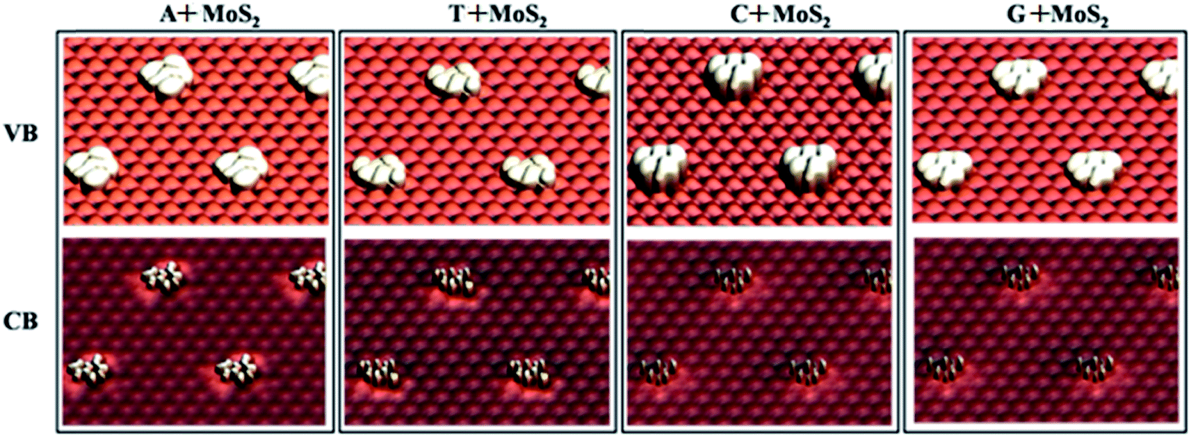 | ||
| Fig. 6 Simulated STM-like topographical images of DNA nucleobase adsorbed on MoS2 for valance band (VB) and conduction band (CB) at biasing of ±1.5 eV between sample and tip. | ||
Next, we looked at the tunneling current characteristics of the nucleobase adsorbed MoS2 within STM like setup shown in Fig. S3 of ESI.† In the STM-like setup, a tip is modeled by a cage-like Au13 cluster. The Bardeen, Tersoff and Hamann (BTH) formalism of electron tunneling was used to calculate the tunneling current in this model setup.46 The biasing is defined as forward bias (or positive bias) when the sample is connected to the positive potential with electrons flowing from tip to sample. The tip is kept at a distance of 4 Å above the nucleobase which describes the non bonding tip sample configuration (Fig. S3†). It is worth mentioning here that the choice of the tip and sample separation defines the magnitude of current as tunneling current is directly proportional to the convolution of DOS between the tip and sample, although the tunneling characteristics remain the same.
The tunneling current characteristics for pristine and nucleobase + MoS2 system have been shown in Fig. 7. We find a rise in tunneling current at a small forward bias of ∼0.7 V for guanine and cytosine adsorbed MoS2. We find the tunneling current more pronounced at ∼1 V which is lower than the value reported by Tanaka et al.47 It is interesting to note that the magnitude of tunneling current increases in negative bias as compared to positive bias which can be attributed to the larger number of unoccupied states in the functionalized monolayers (Fig. 3 and 4). This rise in tunneling current in forward (reverse) bias is attributed to the VB (CB) band offset (Table 2). Note that the rise in tunneling current from zero magnitude depends on the amount of offset taking place upon nucleobase adsorption as far as the type of nucleobase adsorption is concerned.
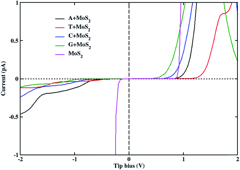 | ||
| Fig. 7 The tunneling current characteristics of A, T, C, G adsorbed MoS2 and pristine MoS2. The distance of separation between tip and sample has been taken as 4 Å. | ||
3.4 Current–voltage characteristics
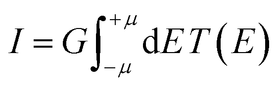
Furthermore, the electron transport through the nucleobase–MoS2 system has been explored with in equilibrium transport theory as implemented in GOLLUM code.48 It uses the DFT generated Hamiltonian as an input and generate the s-matrix and associated physical quantities such as current. The whole device setup is divided into left electrode (LE), scattering region (SR) and right electrode (RE) as shown in Fig. S4.† The applied finite voltage to the electrode change the incoming and outgoing electron distribution and hence Hamiltonian. The modified DFT Hamiltonian can be expressed in the following form:49where, the matrices HL, HR are Hamiltonian for left and right lead, HLM, HRM are interaction Hamiltonian between leads and extended molecule; HM[ρ] represents non equilibrium density matrix derived Hamiltonian; μ (=eV/2) represents the change in energy levels of electrodes; S represents the corresponding overlap matrix blocks between electrode and extended molecule. It is worth mentioning here that the finite bias effects on HM[ρ] are accounted by aligning and de-aligning the molecular orbital's at extended molecular region with shifted electrode energy levels (due to biasing). Therefore, this enables GOLLUM to introduce essential non-equilibrium effects within equilibrium transport theory. Thus the current voltage characteristics (I–V) computed from equilibrium equation

where, G = e/h is the unit of quantum conductance and T(E) is the transmission probability of electron with energy E passing from one electrode to another. Note that STM measurements provide the possibility to probe the electronic structure on a scale unobtainable with other methods on the other hand transport characteristics mimic the possibility of the model in realization of actual devices like FET for sensing application.
The current–voltage (I–V) characteristics for the pristine and nucleobase adsorbed MoS2 is depicted in Fig. 8. An I–V characteristic of pristine MoS2 is almost flat with in the small bias indicating its semiconducting nature. The magnitude of current increases with the increase in applied bias for the pristine as well as the nucleobase + MoS2 complexes. The magnitude of current with applied bias is more in nucleobase + MoS2 complexes as compared to pristine MoS2. The higher magnitude of current in nucleobase complex is due to increase in number of open channels (transmission coefficients) conjugate system as compared to pristine MoS2 (Fig. S5†).
 | ||
| Fig. 8 The current–voltage (I–V) characteristics of pristine MoS2 and A, T, C, G adsorbed MoS2. | ||
Note that the polarization of the pristine MoS2 caused by the DNA nucleobase (Fig. 2) might be the principle cause of small current with in lower bias region. Therefore, these results clearly offer a way to utilize MoS2-based device for DNA sensor.
4. Conclusions
First principle calculations have been carried out for the pristine and nucleobase adsorbed MoS2 using SIESTA code. Following can be concluded from the study:• DNA nucleobase are weakly physisorbed on pristine MoS2 monolayer.
• MoS2 monolayer is considerably polarized upon the adsorption of nucleobase.
• Adsorption of nucleobase leads to offset in the energy levels of pristine nucleobase and MoS2 upon adsorption which causes modification of effective band gap in pristine MoS2.
• The electronic energy band gap is reduced to maximum of 35.62% in guanine + MoS2 complex as compared to pristine MoS2.
• EEL of nucleobase + MoS2 conjugate system is blue shifted by ∼0.58 eV as compared to pristine MoS2.
• The simulated STM measurements give the distinct features for individual nucleobase in STM topograph and tunneling current characteristics.
• Electron transport characteristics (I–V) show large magnitude of current in nucleobase + MoS2 complexes as compared to pristine MoS2 monolayer indicating the possibility of MoS2 for the selective detection of nucleobase.
In nutshell, our study reveals MoS2 monolayer to be strong candidate for the selective bio-sensing of nucleotides.
Acknowledgements
The authors wish to thank Prof. Ravindra Pandey, Michigan Technological University, for his motivation to carry out this work and discussions that proved fruitful. Helpful discussions with Dr Brij Mohan and Rajesh Thakur are highly acknowledged. Munish Sharma wishes to acknowledge the DST, Govt. of India, New Delhi for providing the financial support in the form of INSPIRE Fellowship. CVRAMAN, high performance computing cluster (provided by FIST, DST, Govt. of India, New Delhi) at Physics Department, Himachal Pradesh University has been used to obtain results presented in this paper.References
- T. Ahmed, S. Kilina, T. Das, J. T. Haraldsen, J. J. Rehr and A. V. Balatsky, Nano Lett., 2012, 12, 927–931 CrossRef CAS PubMed.
- S. Gowtham, R. H. Scheicher, R. Pandey, S. P. Karna and R. Ahuja, Nanotechnology, 2008, 19, 125701 CrossRef CAS PubMed.
- T. Kuila, S. Bose, P. Khanra, A. K. Mishra, N. H. Kim and J. H. Lee, Biosens. Bioelectron., 2011, 26, 4637–4648 CrossRef CAS PubMed.
- Y. Shao, J. Wang, H. Wu, J. Liu, I. A. Aksay and Y. Lin, Electroanalysis, 2010, 22, 1027–1036 CrossRef CAS.
- C. Sathe, X. Zou, J.-P. Leburton and K. Schulten, ACS Nano, 2011, 5, 8842–8851 CrossRef CAS PubMed.
- S. Meng, P. Maragakis, C. Papaloukas and E. Kaxiras, Nano Lett., 2007, 7, 45–50 CrossRef CAS PubMed.
- D. Fu and L.-J. Li, Nano Rev., 2010, 1, 5354 CrossRef PubMed.
- D. Sarkar, W. Liu, X. Xie, A. C. Anselmo, S. Mitragotri and K. Banerjee, ACS Nano, 2014, 8, 3992–4003 CrossRef CAS PubMed.
- X. Gan and H. Zhao, Sens. Mater., 2015, 27, 191–215 CAS.
- C.-S. Chou, Y.-C. Wu and C.-H. Lin, RSC Adv., 2014, 4, 52903–52910 RSC.
- S.-W. Fan, A. K. Srivastava and V. P. Dravid, Sens. Actuators, B, 2010, 144, 159–163 CrossRef CAS.
- B. Liu, L. Chen, G. Liu, A. N. Abbas, M. Fathi and C. Zhou, ACS Nano, 2014, 8, 5304–5314 CrossRef CAS PubMed.
- S. Mukhopadhyay, S. Gowtham, R. H. Scheicher, R. Pandey and S. P. Karna, Nanotechnology, 2010, 21, 165703 CrossRef PubMed.
- Z. Wang, H. He, W. Slough, R. Pandey and S. P. Karna, J. Phys. Chem. C, 2015, 119, 25965–25973 CrossRef CAS.
- R. G. Amorim and R. H. Scheicher, Nanotechnology, 2015, 26, 154002 CrossRef PubMed.
- S. K. Vashist and J. H. Luong, Carbon, 2015, 84, 519–550 CrossRef CAS.
- A. B. Farimani, K. Min and N. R. Aluru, ACS Nano, 2014, 8, 7914–7922 CrossRef CAS PubMed.
- G. Korotcenkov, J. Mater. Sci. Eng. B, 2007, 139, 1–23 CrossRef CAS.
- K. Kalantar-Zadeh and J. Z. Ou, ACS Sens., 2016, 1(1), 5–16 CrossRef CAS.
- M. Sharma, P. Jamdagni, A. Kumar and P. K. Ahluwalia, AIP Conf. Proc., 2016, 1731, 140045 CrossRef.
- K. Liu, J. Feng, A. Kis and A. Radenovic, ACS Nano, 2014, 8, 2504–2511 CrossRef CAS PubMed.
- H. S. Kim and Y.-H. Kim, Biosens. Bioelectron., 2015, 69, 186–198 CrossRef CAS PubMed.
- X. Zhang, M. Rahman, D. Neff and M. L. Norton, Beilstein J. Nanotechnol., 2014, 5, 501–506 CrossRef CAS.
- J. Lee, P. Dak, Y. Lee, H. Park, W. Choi, M. A. Alam and S. Kim, Sci. Rep., 2014, 4, 7352 CrossRef CAS PubMed.
- H. Nam, B.-R. Oh, M. Chen, S. Wi, D. Li, K. Kurabayashi and X. Liang, J. Vac. Sci. Tech. B, 2015, 33, 06FG01 CrossRef.
- D. A. Wheeler, M. Srinivasan, M. Egholm, Y. Shen, L. Chen, A. McGuire, W. He, Y.-J. Chen, V. Makhijani and G. T. Roth, Nature, 2008, 452, 872–876 CrossRef CAS PubMed.
- P. Ordejón, E. Artacho and J. M. Soler, Phys. Rev. B: Condens. Matter Mater. Phys., 1996, 53, R10441 CrossRef.
- J. M. Soler, E. Artacho, J. D. Gale, A. García, J. Junquera, P. Ordejón and D. Sánchez-Portal, J. Phys.: Condens. Matter, 2002, 14, 2745 CrossRef CAS.
- M. Sharma, A. Kumar, P. Ahluwalia and R. Pandey, J. Appl. Phys., 2014, 116, 063711 CrossRef.
- M. Sharma, P. Jamdagni, A. Kumar and P. Ahluwalia, Phys. E, 2015, 71, 49–55 CrossRef CAS.
- N. Kumar, M. Sharma, J. Sharma and P. Ahluwalia, Indian J. Phys., 2015, 89, 143–150 CrossRef CAS.
- M. Dion, H. Rydberg, E. Schröder, D. C. Langreth and B. I. Lundqvist, Phys. Rev. Lett., 2004, 92, 246401 CrossRef CAS PubMed.
- G. Román-Pérez and J. M. Soler, Phys. Rev. Lett., 2009, 103, 096102 CrossRef PubMed.
- M. Sharma, G. Loh, G. Wang, R. Pandey, S. P. Karna and P. Ahluwalia, RSC Adv., 2016, 6, 38499–38504 RSC.
- H. Vovusha and B. Sanyal, RSC Adv., 2015, 5, 67427–67434 RSC.
- M. Hosseini, M. Elahi, M. Pourfath and D. Esseni, J. Phys. D: Appl. Phys., 2015, 48, 375104 CrossRef.
- T. Li, Phys. Rev. B: Condens. Matter Mater. Phys., 2012, 85, 235407 CrossRef.
- H. Ramakrishna Matte, A. Gomathi, A. K. Manna, D. J. Late, R. Datta, S. K. Pati and C. Rao, Angew. Chem., 2010, 122, 4153–4156 CrossRef.
- A. Splendiani, L. Sun, Y. Zhang, T. Li, J. Kim, C.-Y. Chim, G. Galli and F. Wang, Nano Lett., 2010, 10, 1271–1275 CrossRef CAS PubMed.
- K. F. Mak, C. Lee, J. Hone, J. Shan and T. F. Heinz, Phys. Rev. Lett., 2010, 105, 136805 CrossRef PubMed.
- M.-H. Chiu, C. Zhang, H.-W. Shiu, C.-P. Chuu, C.-H. Chen, C.-Y. S. Chang, C.-H. Chen, M.-Y. Chou, C.-K. Shih and L. J. Li, Nat. Commun., 2015, 6, 7666 CrossRef CAS PubMed.
- Y. Li, A. Chernikov, X. Zhang, A. Rigosi, H. M. Hill, A. M. van der Zande, D. A. Chenet, E.-M. Shih, J. Hone and T. F. Heinz, Phys. Rev. B: Condens. Matter Mater. Phys., 2014, 90, 205422 CrossRef.
- J. Tersoff and D. Hamann, Phys. Rev. Lett., 1983, 50, 1998 CrossRef CAS.
- R. M. Feenstra, J. A. Stroscio and A. Fein, Surf. Sci., 1987, 181, 295–306 CrossRef CAS.
- I. Horcas, R. Fernández, J. Gomez-Rodriguez, J. Colchero, J. Gómez-Herrero and A. Baro, Rev. Sci. Instrum., 2007, 78, 013705 CrossRef CAS PubMed.
- D. Tománek and S. G. Louie, Phys. Rev. B: Condens. Matter Mater. Phys., 1988, 37, 8327 CrossRef.
- H. Tanaka and T. Kawai, Nat. Nanotechnol., 2009, 4, 518–522 CrossRef CAS PubMed.
- J. Ferrer, C. J. Lambert, V. M. García-Suárez, D. Z. Manrique, D. Visontai, L. Oroszlany, R. Rodríguez-Ferradás, I. Grace, S. Bailey and K. Gillemot, New J. Phys., 2014, 16, 093029 CrossRef.
- V. M. García-Suárez and J. Ferrer, Phys. Rev. B: Condens. Matter Mater. Phys., 2012, 86, 125446 CrossRef.
Footnote |
| † Electronic supplementary information (ESI) available. See DOI: 10.1039/c6ra10008b |
| This journal is © The Royal Society of Chemistry 2016 |