DOI:
10.1039/C6RA09606A
(Paper)
RSC Adv., 2016,
6, 55064-55070
Fabrication and ionic transportation characterization of funnel-shaped nanochannels†
Received
13th April 2016
, Accepted 23rd May 2016
First published on 25th May 2016
Abstract
Solid-state nanochannels have attracted increasing interest because they exhibit similar properties to, but are more stable than, biological nanopores. However, existing solid-state nanochannels, such as conical-shaped nanochannels, possess a limited critical region at the tip side, and thus demonstrate poor controllability of the orientation and magnitude of ionic rectification. In this work, we demonstrate the fabrication of funnel-shaped nanochannels with a gradual structural transformation. The longer critical regions can be controlled by tuning the etching temperature. In addition, the rectification ratio can be increased from about 3 to 6 by introducing a longer critical region. Using finite-element analysis based on the Poisson–Nernst–Planck (PNP) equations, it can be found that the increased length of the critical region could contribute to the asymmetric ion transportation. The funnel-shaped nanochannels with enhanced asymmetric ion transportation may find applications in the fields of materials, electronics, and life sciences.
Introduction
Biological nanochannels play key roles in basic biochemical processes in living systems,1 which are realized mainly by three characteristic features: ionic selectivity, ionic rectification and ionic gating. Inspired by protein channels, various solid-state nanopores and nanochannels have been fabricated and functionalized to recreate these functions, in order to simulate the process of ionic transport in living organisms.2–7 Previous works have shown that ion current rectification and permselectivity in confined channels are a consequence of electrostatic interactions between the substrate of the channel and the electrolyte solution.8 Under asymmetric conditions (i.e., an asymmetric-shaped channel or a symmetric channel with asymmetric surface charges), the internal potential has been shown to be asymmetric. Thus, ions with the opposite charge to the substrate would accumulate near the channel surface, but the distribution would be non-uniform along the axis due to the asymmetric channel structure. Considering the match between Debye length and the diameter of the channel, this non-uniformity is a prerequisite for traditional fluidic diodes based on asymmetric nanochannels. But under symmetric conditions (i.e., a cylindrical channel), a Debye length on the order of the nanochannel diameter does not result in ion current rectification due to the lack of broken symmetry in their electrochemical potential. Therefore, asymmetric properties (i.e., asymmetric shape, surface charges and wettability) of the nanochannels are the foundations of rectification and permselectivity. To date, various approaches and materials have been proposed to construct and functionalize solid-state nanopores and nanochannels to meet the requirements for ion current rectification and permselectivity, which are the basis of sensing, energy transition, and filtration.9–13
Early work in this field started with the α-hemolysin protein nanochannel, which consists of a single protein nanochannel embedded within a lipid bilayer membrane.14–16 Protein-based nanochannels and the surrounding lipid bilayers can become unstable if external parameters such as pH, salt concentration, temperature and mechanical stress are changed. Hence research has increasingly focused on solid-state nanochannels, due to their high stability, durability, shape-controllability and tailorable surface properties. The most widely used materials for nanochannels are polymers, such as polycarbonate (PC),17,18 polyethylene terephthalate (PET)19–21 and polyimide (PI),22–24 silicon nitride,25–27 silicon,28,29 and glass.30,31 To date, a variety of approaches have been used to prepare abiotic nanochannels for resistive-pulse sensing, including track-etching,32,33 focused ion beam sculpting,27,34 electron-beam lithography,34 soft lithography35,36 and film embedding of carbon nanotubes.37 Among these, the track-etching method for polymer solid-state nanochannels has proved to be a surprisingly versatile tool for contemporary biotechnology and has been used to fabricate both symmetric and asymmetric solid-state nanochannels. Different shapes of nanochannels, such as cylindrical,38,39 hourglass-shaped,40,41 cigar-shaped,42–44 bullet-shaped,45,46 conical,22,47–49 funnel-shaped,50–52 and dumbbell-shaped nanochannels have been prepared by controlling the potential difference and by adding surfactants or organic solvents to the etching solution during the etching process. However, previously reported nanochannels, such as conical nanochannels, possess only a short critical region at the tip, and thus demonstrate poor controllability of the orientation and magnitude of ionic rectification.51,53–55 Therefore, it is necessary to fabricate a novel solid-state nanochannel system with a longer critical region by precise control of its asymmetric shape, to achieve more complicated functions.
Herein, we fabricated funnel-shaped nanochannels comprised of three parts: a conical segment, a spout and a cylindrical segment (Fig. 1a). By controlling the etching temperature, the position of the spout can be tuned precisely. In practical terms, the length of the conical segment was observed to be longer than 10 μm, the majority of the 12 μm thickness of the PET film, while the cylindrical segment was confined to less than 2 μm long. Meanwhile, the diameters of the large openings at the base side and the cone angles of the conical segments increased with increasing etching temperature. These funnel-shaped nanochannels exhibited superior asymmetric ion transportation properties compared with conical nanochannels, which was further proved by finite-element analysis based on the Poisson–Nernst–Planck (PNP) equations.
 |
| | Fig. 1 (a) Scheme of funnel-shaped nanochannels in PET film and the internal surface properties. (b) SEM images of the cross section of the funnel-shaped nanochannels, and an enlarged image of a cylindrical segment. (c) SEM image of the base side of the funnel-shaped nanochannels and an enlarged image. (d) SEM images of the tip side of the funnel-shaped nanochannels and an enlarged image. | |
Experiments
Polyethylene terephthalate (PET) membrane preparation
Polymer foils of polyethylene terephthalate (PET) (Hostaphan RN 12, Hoechst, density of 2 × 107 cm−2) with 12 μm thickness were irradiated at the linear accelerator UNILAC (GSI, Darmstadt) with swift heavy ions (Au) having an energy of 11.4 MeV per nucleon. The fabrication of nanochannels in the PET membrane was accomplished by asymmetric etching of the damage trail of the heavy ions which passed through the membrane. Before the chemical etching process, the polymer films were exposed to UV light (365 nm, 20 W) for 1 h from each side.
Fabrication of the funnel-shaped nanochannels
The fabrication and current–voltage (I–V) recording device is shown in Fig. S1.† In the fabrication process, the device was heated to control the etching temperature. The following solutions were used as etching and stopping solutions for the etching of PET: 9 M NaOH for etching, 1 M KCl + 1 M HCOOH for stopping. The etching process was carried out at different temperatures (25 °C, 30 °C, 40 °C, 50 °C, 60 °C). First, the track-etched membrane was mounted between two halves of a conductivity cell, and Pt electrodes were used to apply a transmembrane potential. Then one half of the cell was filled with etching solution while the other was filled with stopping solution. During etching, a potential of 1 V was applied across the membrane in order to monitor the breakthrough of the nanochannel and observe the current flowing through the nascent nanochannels. The current remained zero as long as the channel is not yet etched through, and after the breakthrough an increase of current was observed. The etching process was stopped when the current reached a certain value. The membrane was then soaked in MilliQ water (18.2 MΩ) to remove residual salts.
Current measurement
The ionic transport properties of the nanochannels were studied by measuring ionic current through the multinanochannels. Ionic current was measured with a Keithley 6487 picoammeter (Keithley Instruments, Cleveland, OH). The funnel-shaped nanochannel membrane was mounted between two chambers of the etching cell mentioned above. The I–V curves were adjusted to zero current at zero voltage to remove small offsets experienced between runs. All measurements were carried out at room temperature, and I–V behaviour was examined with 0.1 M KCl neutral aqueous solution. In all experiments, Ag/AgCl electrodes were used to apply a transmembrane potential across the film, with the positive electrode placed at the base of the funnel-shaped nanochannels and the negative electrode at the tip. The main transmembrane potential used in this work was stepped at 0.2 V per step for 1 s per step (0.2 V s−1) from −2 to +2 V, with a period of 40 s.
Results and discussion
Morphology of the funnel-shaped nanochannels
The dimension and morphology of the funnel-shaped nanochannels were characterized by scanning electron microscopy (SEM). Fig. 1b–d shows the SEM images of the fracture and the surface of the funnel-shaped nanochannels etched at 40 °C. Fig. 1b shows the cross section of funnel-shaped nanochannels and an enlarged image of a cylindrical segment. It can be clearly observed that the asymmetric nanochannel consists of a conical segment and a cylindrical segment. The base side of the conical segment is about 1000 nm in diameter, while the diameter of the cylindrical segment is about 15 nm. Fig. 1c illustrates the top view of the base side of the funnel-shaped nanochannels and an enlarged image, which shows the tapering of the conical segment. Fig. 1d shows the top view of the tip side of the nanochannels and an enlarged image. The tip diameter is about 15 nm, which is equal to the diameter of the cylindrical segment. These results complement the results for the cross sections of the funnel-shaped nanochannel, and verify the transformation from a conical structure to a cylindrical segment indirectly.
Funnel-shaped nanochannels with varied etching temperatures
Five funnel-shaped nanochannels with different geometries were prepared under etching temperatures of 25 °C, 30 °C, 40 °C, 50 °C, and 60 °C. By adjusting the etching temperature, the base side diameter, the cone angle and the spout position of the funnel-shaped nanochannels could be precisely controlled (Fig. 2a). Fig. 2b–f show the SEM images of the top views and cross sections of these funnel-shaped nanochannels. The difference in base diameters (Fig. 2bi–fi) and cone angles (Fig. 2bii–fii) of the nanochannels prepared under different etching temperatures can clearly be observed. The diameters of the base sides increased from ∼800 nm to ∼1400 nm (Fig. 3a), while the cone angles increased from ∼3.9° to ∼7.8° (Fig. 3b) as the etching temperature increased from 25 °C to 60 °C. Table S1† shows the statistical diameters and cone angles, which were analyzed based on SEM images. The tip diameters could be calculated using eqn (1):56| |
 | (1) |
where VB and VT are the bulk-etching speed and track-etching speed, DT and DB are the tip and base diameters, k is the specific conductivity of the electrolyte, and U and I are the applied voltage and measured ionic current from the pore conductivity measurements, respectively. The calculated tip diameters also increased along with the increasing etching temperature from ∼12 nm to ∼20 nm, which is consistent with the results of SEM (Fig. 2biii–fiii).
 |
| | Fig. 2 (a) Schematic diagram of the transition of asymmetric nanochannels from conical-shaped to funnel-shaped by changing the etching temperature. (b–f) SEM images of the funnel-shaped nanochannels with varying temperature (left to right: 25 °C, 30 °C, 40 °C, 50 °C, 60 °C). (i): top view; (ii): cross section (scale bar 100 nm); (iii): enlarged cylindrical segments. | |
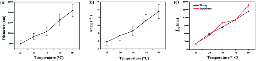 |
| | Fig. 3 (a) The variation of the base diameter of the conical segment of the funnel-shaped nanochannel with temperature. (b) The variation of the conical angle of the conical segment of the funnel-shaped nanochannel with temperature. (c) The location of the spout observed from SEM images (experiment: red line) and calculated by the model (theory: dark line). | |
Furthermore, the length of the cylindrical segment, which can be represented by the distance between spout and the tip of the nanochannel, can also be obtained from the SEM images. Below 25 °C, the cylindrical segment of the funnel-shaped nanochannel was about 220 nm, which is negligible compared with the length of the entire channel. That is to say, this nanochannel approximately cone-shaped. The length of the cylindrical segment increased along with the etching temperature, reaching 515 nm, 1000 nm, 1114 nm and 1979 nm for the channels created at 30 °C, 40 °C, 50 °C and 60 °C, respectively (Fig. 3c, red line). In order to further prove the relationship between the spout position and etching temperature, we suggested a theoretical model for these funnel-shaped asymmetric nanochannels. The following formula was used to calculate the location of the transition point:
| |
 | (2) |
where
L is the entire length of the channel,
L1 is the length of the cone,
L2 is the distance between the tip side and the transition point,
α is the angle of the conical segment, and
DB and
DT are the base and tip diameters of the conical segment. Then a quantitative relationship between the length of the cylindrical segment
L2 and the parameters
DB,
DT and
α of the conical segment can be established through
eqn (2). Theoretical calculations show that the spout is close to the tip side (about 220 nm from tip side) at relatively low temperature (25 °C). When the temperature rose to 60 °C, the length of the cylindrical segment increased to about 1900 nm, and the length of the cylindrical segment increased almost linearly with the increasing etching temperature (
Fig. 3c, black line), which could be reproduced by the experimental curves obtained from SEM images.
The relationship between the track-etching velocity and the etching temperature, which can be characterized by measuring the breakthrough ionic current in the track-etching process, has also been studied. Fig. 4 shows the changes in track-etching velocity with the etching temperature ranging from 25 °C to 60 °C in three parallel experiments. The etching velocities were 0.21 μm min−1, 0.58 μm min−1, 0.82 μm min−1, 1.21 μm min−1, and 2.3 μm min−1 at 25 °C, 30 °C, 40 °C, 50 °C, and 60 °C, respectively, which matched a binomial simulation (Fig. 4, black line). This nonlinear increase indicates indirectly that the cylindrical segment will be longer if the etching temperature is higher.
 |
| | Fig. 4 Relationship between the etching velocity and the temperature (25 °C, 30 °C, 40 °C, 50 °C, 60 °C). The red square  , blue circle , blue circle  and green triangle and green triangle  represent three parallel experiments. Black line is the polynomial simulation curve. represent three parallel experiments. Black line is the polynomial simulation curve. | |
Etching mechanism
The etching mechanism is schematically shown in Fig. 5a and b. At low temperature (25 °C), the VLT (low temperature track-etching velocity) along the direction of the damage trail is faster than the VLB (low temperature bulk-etching velocity) in the direction perpendicular to the damage trail of heavy ions which passed through the membrane. After a short breakthrough time, the etching process was stopped before the alkali diffused to the region beyond the damage trail. Hence, a small cylindrical segment was formed at the tip side of the nanochannel (Fig. 5a). At high temperature (60 °C), the VHT (high temperature track-etching velocity) is much faster than the VLT and VHB (high temperature bulk-etching velocity), and the etching process was stopped as soon as breakthrough was achieved, which means that there is not enough time for the tip side to be etched, and thus a longer cylindrical segment was obtained (Fig. 5b). In fact, the etching rate ratio (VLT/VLB) was as much as 1000 under low temperature conditions (25 °C), while a high temperature further increased the etching rate ratio (VHT/VHB). Hence, funnel-shaped nanochannels with different cylindrical segments can be generated by changing the etching temperature.
 |
| | Fig. 5 (a) Schematic of etched ion tracks in a low temperature environment. (b) Schematic of etched ion tracks in a high temperature environment. | |
Ionic transport properties
The ionic transport properties of these funnel-shaped nanochannels were examined by current measurements. The transmembrane ionic current was recorded under symmetrical electrical conditions using 0.1 M KCl (pH ≈ 7) solution in both halves of the conductivity cell. Fig. 6a shows the I–V properties of funnel-shaped nanochannels that were prepared under different etching temperatures from 25 °C to 60 °C, from which it can be seen that the I–V curves associated with ionic migration through these nanochannels are nonlinear. The ion-current rectification properties of these funnel-shaped nanochannels have been observed previously in a variety of asymmetrical nanochannels and nanotubes, and experiments prove that ion-current rectification is linked to asymmetry, e.g., conical nanochannel systems with excess surface charge.57,58 The extent to which the funnel-shaped nanochannel rectifies the ion current flowing through it can be quantified by the rectification ratio, defined as the absolute value of the current obtained at −2 V divided by the current obtained at +2 V. Clearly, the rectification ratios increased gradually from about 3 to 6 along with the increasing etching temperature (Fig. 6b, blue line). In the conical nanochannel, only weak ion-rectifying behaviour was observed because the transport properties are determined by the physical and chemical properties of the nanoscale critical point (tip side) of the channel. Nevertheless, with an increased critical region, the cylindrical segment has tremendous potential for ion selectivity and can enhance the rectification ratio.
 |
| | Fig. 6 (a) Current–voltage curves for funnel-shaped nanochannels formed at different temperatures. (b) Ion current at constant voltage (−2 V) and rectification ratio of the funnel-shaped nanochannels formed at different temperatures. | |
Meanwhile, the ion current at constant voltage (−2 V) decreased significantly from 3.2 μA to 1.5 μA (Fig. 6b, dark line) as the etching temperature increased. This also can be explained by the length of the cylindrical segment, which is comparable to the Debye length.50,51 In the nanochannel, the charged nanosized crucial region (the tip side of the conical and the cylindrical segment of the funnel-shaped nanochannel) can adsorb the counter-ions in the electrolyte, and block the ion transportation. The resistance of the ions is proportional to the length of the cylindrical segment because of the interactions with charged channel wall. As a result, funnel-shaped nanochannels with longer critical regions have a smaller ionic current.
Theoretical calculations based on Poisson–Nernst–Planck (PNP)
Previous works have shown that ion current rectification observed in nanochannels is dependent on three conditions: the accordance between the diameter of the channel and the length of the electrical double layer, the excess surface charge, and the interactions of ions with the pore wall.59–61 To gain further understanding of ion transportation in the funnel-shaped nanochannels, a model based on the Poisson–Nernst–Planck (PNP) equations is used to quantitatively describe the ion current in the nanochannel.57,62,63 Finite-element analysis was performed to simultaneously solve the PNP equations for the ion concentration to better understand the shape-dependent I–V behaviours (Fig. S2†). The concentration distribution of the ions (K+ and Cl−) visually reflects the rectification ratio because the rectification effect stems from the accumulation and depletion of ions in the channel in response to different bias polarities. As shown in Fig. 7a, it can be clearly observed that both the K+ and Cl− concentrations under −2 V are higher than under +2 V for the conical-shaped nanochannels, because the ions accumulate under negative voltage, resulting in high ion conduction. On the contrary, reversing the direction of the applied electric field moves the ions in the outward direction from the channel, causing the formation of a depletion zone and, consequently, a very low conductance of the nanochannel, which generates the rectification of ion current. The concentration distribution of the funnel-shaped nanochannels is similar to that of the conical-shaped nanochannels, but more ions would accumulate in the spout and the longer cylindrical segment, which is comparable to the Debye length, (Fig. 7b) thus leading to a higher rectification ratio. In addition, the negatively charged nanosized critical region (the tip side of the conical and the cylindrical segment of the funnel-shaped nanochannel) can adsorb the counter-ions (K+) in the electrolyte, hence, the K+ concentrations are higher than the Cl− concentrations both in the conical and funnel-shaped nanochannel. Therefore, the ion concentration distributions simulated by finite-element simulations can provide direct and strong evidence for our experimental results, which also have important ramifications for the application of such funnel-shaped nanochannels in biosensor designs.
 |
| | Fig. 7 (a) Concentration profiles (K+ and Cl−) of numerical simulations of a 2D configuration of the conical-shaped nanochannel under −2 V and +2 V. (b) Concentration profiles (K+ and Cl−) of numerical simulations of a 2D configuration of the funnel-shaped nanochannel under −2 V and +2 V. | |
Conclusions
In summary, we have shown that the funnel-shaped nanochannels with a gradual structural transformation can be fabricated by changing the track-etching temperature. The funnel-shaped nanochannels consist of three parts, the conical segment, the cylindrical segment and the spout that connects the conical segment and the cylindrical segment. The spout position can be controlled by adjusting the etching temperature. Most importantly, the rectification ratio can be increased from about 3 to 6 by introducing the longer critical region. Additionally, finite-element analysis agrees well with the experimental results. Such funnel-shaped nanochannels may find applications in the fields of materials, electronics, and life sciences.
Acknowledgements
This work was supported by the National Research Fund for Fundamental Key Projects (2013CB933000), the National Natural Science Foundation (21434003, 91427303, 21421061), and the Key Research Program of the Chinese Academy of Sciences (KJZD-EW-M03). The authors thank the Material Science Group of GSI for providing the ion-irradiated samples.
Notes and references
- B. Hille, Ion channels of excitable membranes, Sinauer, Sunderland, MA, 2001 Search PubMed.
- K. Xiao, X.-Y. Kong, Z. Zhang, G. Xie, L. Wen and L. Jiang, J. Photochem. Photobiol., C, 2016, 26, 31–47 CrossRef CAS.
- L. Wen, Y. Tian and L. Jiang, Angew. Chem., Int. Ed., 2015, 54, 3387–3399 CrossRef CAS PubMed.
- S. J. Kim, Y.-A. Song and J. Han, Chem. Soc. Rev., 2010, 39, 912–922 RSC.
- H. Daiguji, Chem. Soc. Rev., 2010, 39, 901–911 RSC.
- R. E. Gyurcsányi, TrAC, Trends Anal. Chem., 2008, 27, 627–639 CrossRef.
- C. R. Martin and Z. S. Siwy, Science, 2007, 317, 331–332 CrossRef CAS PubMed.
- I. Vlassiouk and Z. S. Siwy, Nano Lett., 2007, 7, 552–556 CrossRef CAS PubMed.
- J.-Y. Lin, C.-Y. Lin, J.-P. Hsu and S. Tseng, Anal. Chem., 2016, 88, 1176–1187 CrossRef CAS PubMed.
- Z. Zhang, X.-Y. Kong, K. Xiao, Q. Liu, G. Xie, P. Li, J. Ma, Y. Tian, L. Wen and L. Jiang, J. Am. Chem. Soc., 2015, 137, 14765–14772 CrossRef CAS PubMed.
- L. Wen, K. Xiao, A. V. Sainath, M. Komura, X. Y. Kong, G. Xie, Z. Zhang, Y. Tian, T. Iyoda and L. Jiang, Adv. Mater., 2016, 28, 757–763 CrossRef CAS PubMed.
- M. Fujiwara and T. Imura, ACS Nano, 2015, 9, 5705–5712 CrossRef CAS PubMed.
- J. D. Feng, K. Liu, R. D. Bulushev, S. Khlybov, D. Dumcenco, A. Kis and A. Radenovic, Nat. Nanotechnol., 2015, 10, 1070–1076 CrossRef CAS PubMed.
- T. Li, L. Liu, Y. R. Li, J. N. Xie and H. C. Wu, Angew. Chem., Int. Ed., 2015, 54, 7568–7571 CrossRef CAS PubMed.
- J. J. Kasianowicz, E. Brandin, D. Branton and D. W. Deamer, Proc. Natl. Acad. Sci. U. S. A., 1996, 93, 13770–13773 CrossRef CAS.
- J. E. Gouaux, O. Braha, M. R. Hobaugh, L. Song, S. Cheley, C. Shustak and H. Bayley, Proc. Natl. Acad. Sci. U. S. A., 1994, 91, 12828–12831 CrossRef CAS.
- C. C. Harrell, Y. Choi, L. P. Horne, L. A. Baker, Z. S. Siwy and C. R. Martin, Langmuir, 2006, 22, 10837–10843 CrossRef CAS PubMed.
- C. Schönenberger, B. Van der Zande, L. Fokkink, M. Henny, C. Schmid, M. Krüger, A. Bachtold, R. Huber, H. Birk and U. Staufer, J. Phys. Chem. B, 1997, 101, 5497–5505 CrossRef.
- P. Y. Apel, I. V. Blonskaya, O. L. Orelovitch, P. Ramirez and B. A. Sartowska, Nanotechnology, 2011, 22, 175302 CrossRef PubMed.
- K. Xiao, G. Xie, P. Li, Q. Liu, G. Hou, Z. Zhang, J. Ma, Y. Tian, L. Wen and L. Jiang, Adv. Mater., 2014, 26, 6560–6565 CrossRef CAS PubMed.
- M. Ali, S. Nasir and W. Ensinger, Chem. Commun., 2015, 51, 3454–3457 RSC.
- L. P. Wen, Q. Liu, J. Ma, Y. Tian, C. H. Li, Z. S. Bo and L. Jiang, Adv. Mater., 2012, 24, 6193–6198 CrossRef CAS PubMed.
- A. Mara, Z. Siwy, C. Trautmann, J. Wan and F. Kamme, Nano Lett., 2004, 4, 497–501 CrossRef CAS.
- Z. Siwy, D. Dobrev, R. Neumann, C. Trautmann and K. Voss, Appl. Phys. A: Mater. Sci. Process., 2003, 76, 781–785 CrossRef CAS.
- D. J. Niedzwiecki, R. Iyer, P. N. Borer and L. Movileanu, ACS Nano, 2013, 7, 3341–3350 CrossRef CAS PubMed.
- A. Han, M. Creus, G. Schürmann, V. Linder, T. R. Ward, N. F. de Rooij and U. Staufer, Anal. Chem., 2008, 80, 4651–4658 CrossRef CAS PubMed.
- J. Li, D. Stein, C. McMullan, D. Branton, M. J. Aziz and J. A. Golovchenko, Nature, 2001, 412, 166–169 CrossRef CAS PubMed.
- R. Kox, C. Chen, G. Maes, L. Lagae and G. Borghs, Nanotechnology, 2009, 20, 115302 CrossRef PubMed.
- S. R. Park, H. Peng and X. S. Ling, Small, 2007, 3, 116–119 CrossRef CAS PubMed.
- N. Laohakunakorn, V. V. Thacker, M. Muthukumar and U. F. Keyser, Nano Lett., 2015, 15, 695–702 CrossRef CAS PubMed.
- G. Wang, A. K. Bohaty, I. Zharov and H. S. White, J. Am. Chem. Soc., 2006, 128, 13553–13558 CrossRef CAS PubMed.
- P. Y. Apel, I. V. Blonskaya, S. N. Dmitriev, O. L. Orelovitch, A. Presz and B. A. Sartowska, Nanotechnology, 2007, 18, 305302 CrossRef.
- P. Apel, Radiat. Meas., 2001, 34, 559–566 CrossRef CAS.
- A. Storm, J. Chen, X. Ling, H. Zandbergen and C. Dekker, Nat. Mater., 2003, 2, 537–540 CrossRef CAS PubMed.
- O. A. Saleh and L. L. Sohn, Nano Lett., 2003, 3, 37–38 CrossRef CAS.
- J. Han and H. Craighead, Science, 2000, 288, 1026–1029 CrossRef CAS PubMed.
- L. Liu, C. Yang, K. Zhao, J. Li and H.-C. Wu, Nat. Commun., 2013, 4, 2989 Search PubMed.
- N. Liu, Y. Jiang, Y. Zhou, F. Xia, W. Guo and L. Jiang, Angew. Chem., Int. Ed., 2013, 52, 2007–2011 CrossRef CAS PubMed.
- Q. H. Nguyen, M. Ali, V. Bayer, R. Neumann and W. Ensinger, Nanotechnology, 2010, 21, 365701 CrossRef PubMed.
- X. Hou, F. Yang, L. Li, Y. L. Song, L. Jiang and D. B. Zhu, J. Am. Chem. Soc., 2010, 132, 11736–11742 CrossRef CAS PubMed.
- X. Hou, Y. J. Liu, H. Dong, F. Yang, L. Li and L. Jiang, Adv. Mater., 2010, 22, 2440–2443 CrossRef CAS PubMed.
- H. Zhang, X. Hou, L. Zeng, F. Yang, L. Li, D. Yan, Y. Tian and L. Jiang, J. Am. Chem. Soc., 2013, 135, 16102–16110 CrossRef CAS PubMed.
- M. Ali, P. Ramirez, H. Q. Nguyen, S. Nasir, J. Cervera, S. Mafe and W. Ensinger, ACS Nano, 2012, 6, 3631–3640 CrossRef CAS PubMed.
- P. Y. Apel, I. Blonskaya, A. Y. Didyk, S. Dmitriev, O. Orelovitch, D. Root, L. Samoilova and V. Vutsadakis, Nucl. Instrum. Methods Phys. Res., Sect. B, 2001, 179, 55–62 CrossRef CAS.
- P. Y. Apel, I. Blonskaya, O. Orelovitch and S. Dmitriev, Nucl. Instrum. Methods Phys. Res., Sect. B, 2009, 267, 1023–1027 CrossRef CAS.
- Y. Xie, X. Wang, J. Xue, K. Jin, L. Chen and Y. Wang, Appl. Phys. Lett., 2008, 93, 163116 CrossRef.
- Z. P. Zeng, Y. Ai and S. Z. Qian, Phys. Chem. Chem. Phys., 2014, 16, 2465–2474 RSC.
- X. Hou, H. Dong, D. Zhu and L. Jiang, Small, 2010, 6, 361–365 CrossRef CAS PubMed.
- P. Y. Apel, Y. E. Korchev, Z. Siwy, R. Spohr and M. Yoshida, Nucl. Instrum. Methods Phys. Res., Sect. B, 2001, 184, 337–346 CrossRef CAS.
- K. Xiao, G. Xie, Z. Zhang, X. Y. Kong, Q. Liu, P. Li, L. Wen and L. Jiang, Adv. Mater., 2016, 28, 3345–3350 CrossRef CAS PubMed.
- Q. H. Nguyen, M. Ali, S. Nasir and W. Ensinger, Nanotechnology, 2015, 26, 485502 CrossRef PubMed.
- D. Mo, J. D. Liu, J. L. Duan, H. J. Yao, H. Latif, D. L. Cao, Y. H. Chen, S. X. Zhang, P. F. Zhai and J. Liu, Nucl. Instrum. Methods Phys. Res., Sect. B, 2014, 333, 58–63 CrossRef CAS.
- J. M. Perry, K. Zhou, Z. D. Harms and S. C. Jacobson, ACS Nano, 2010, 4, 3897–3903 CrossRef CAS PubMed.
- L. Gao, P. Li, Y. Zhang, K. Xiao, J. Ma, G. Xie, G. Hou, Z. Zhang, L. Wen and L. Jiang, Small, 2015, 11, 543–549 CrossRef CAS PubMed.
- Y. Shang, Y. Zhang, P. Li, J. Lai, X.-Y. Kong, W. Liu, K. Xiao, G. Xie, Y. Tian and L. Wen, Chem. Commun., 2015, 51, 5979–5982 RSC.
- P. Y. Apel, I. V. Blonskaya, O. L. Orelovitch, B. A. Sartowska and R. Spohr, Nanotechnology, 2012, 23, 225503 CrossRef PubMed.
- I. Vlassiouk, S. Smirnov and Z. Siwy, ACS Nano, 2008, 2, 1589–1602 CrossRef CAS PubMed.
- R. Karnik, C. Duan, K. Castelino, H. Daiguji and A. Majumdar, Nano Lett., 2007, 7, 547–551 CrossRef CAS PubMed.
- Z. Siwy, I. Kosińska, A. Fuliński and C. Martin, Phys. Rev. Lett., 2005, 94, 048102 CrossRef CAS PubMed.
- I. Kosińska and A. Fuliński, Phys. Rev. E: Stat., Nonlinear, Soft Matter Phys., 2005, 72, 011201 CrossRef PubMed.
- D. Stein, M. Kruithof and C. Dekker, Phys. Rev. Lett., 2004, 93, 035901 CrossRef PubMed.
- E. R. Cruz-Chu, T. Ritz, Z. S. Siwy and K. Schulten, Faraday Discuss., 2009, 143, 47–62 RSC.
- J. Cervera, B. Schiedt and P. Ramirez, Europhys. Lett., 2005, 71, 35 CrossRef CAS.
Footnote |
| † Electronic supplementary information (ESI) available. See DOI: 10.1039/c6ra09606a |
|
| This journal is © The Royal Society of Chemistry 2016 |
Click here to see how this site uses Cookies. View our privacy policy here. 


 , blue circle
  and green triangle
  represent three parallel experiments. Black line is the polynomial simulation curve.

