DOI:
10.1039/C6RA09580A
(Paper)
RSC Adv., 2016,
6, 56963-56970
Tunable and ultra-broad plasmon enhanced upconversion emission of NaYF4:Yb3+, Er3+ nanoparticles deposited on Au films with papilla Au nanoparticles
Received
13th April 2016
, Accepted 6th June 2016
First published on 7th June 2016
Abstract
Rare earth ions doped upconversion nanoparticles have broad applications ranging from biological imaging to solar energy conversion. However, the application of upconversion nanoparticles has been limited due to their low upconversion efficiencies. In this paper, two kinds of Au films with tunable and broad surface plasmonic absorptions were used to enhance the upconversion emission of NaYF4:Yb3+, Er3+ nanoparticles, respectively. The results demonstrated that the upconversion enhancement is highly dependent on the topography of Au films. About 77 and 40-fold enhancement were obtained for the green and red UC emissions of NaYF4:Yb3+, Er3+ nanoparticles on the irregular and random Au particles. About 121 and 78-fold enhancement were obtained for the green and red UC emissions of NaYF4:Yb3+, Er3+ nanoparticles on continuous Au films with papilla Au nanoparticles, respectively. In contrast to that of NaYF4:Yb3+, Er3+ nanoparticles deposited on quartz substrate, and the corresponding UC efficiency of NaYF4:Yb3+, Er3+ nanoparticles on irregular and random Au particles and continuous Au films with papilla Au nanoparticles increased by 50% and 100%, respectively. The enhancement of UC emission may be attributed to the increase of radiative decay rate and the enhancement of excitation field.
1. Introduction
Rare earth doped upconversion (UC) nanocrystals can convert two or more photons with lower energy into one photon with higher energy, and have unique potential applications in biological assays and medical imaging due to their sharp emission bandwidths, large anti-Stokes shifts, low auto-fluorescence background and high penetration depth.1–7 However, the UC emissions of rare earth doped nanocrystals mainly are attributed to the parity-forbidden 4f–f electron transitions, resulting in their low UC emission efficiencies. For example, hexagonal phase NaYF4 nanocrystals co-doped with Yb3+ and Er3+ has been commonly considered as one of the most effective UC materials.8–10 However, its UC quantum efficiency is only 0.005% (at 150 W cm−2) when the particle size is 8–10 nm under 980 nm excitation.10 Therefore, approaches to improve UC emission from rare earth doped nanocrystals are of particular interest for their application. In recent years, researchers have developed several effective methods for enhancing the efficiency of UC emission of nanoparticles, including a host lattice selection with low phonon energy, amorphous shell coating on the surface of UC nanocrystals, photonic crystals surface effect, and surface plasmon enhancement caused by metal nanocrystals.11–14
Localized surface plasmon (LSP) occurs around the metal nanoparticles due to free electrons oscillate, which can be coupled with UC emission light of rare earth ions doped nanocrystals and excitation light. Thus the localized surface plasmon of metal nanocrystals was proposed as a convenient approach for increasing the efficiency of UC emission.15,16 At present, considerable investigation have been done about influence of LSP of metal nanocrystals on the UC emission of nanocrystals. For example, Yan group reported an obvious enhancement in the UC emission intensity by LSP for the first time.17 The 2.3 and 3.7 enhancement factors were obtained for green and red UC emissions, respectively. Duan group demonstrated a more than 150% increasing of the blue UC emission intensity in the NaYF4:Yb3+, Tm3+ nanoparticles attached to Au nanoparticles.18 Another works obtained an average 5.1 factor enhancement of UC emission in NaYF4:Yb3+, Er3+ nanoparticles caused by gold island films. In the metal nanostructures enhanced UC emission, the established guiding principle is that the overlapping between the surface plasmon absorption peak and 980 nm excitation light or UC emission wavelength of the nanoparticles is required. However, in the previous works, the LSP bands of metal structures overlapped with either the near infrared absorption or visible UC emission bands due to the larger energy separation between the absorbing and UC emission bands of rare earth ions.19,20 This severely limits its enhancement factor because the surface plasmon of metal nanoparticles cannot couple simultaneously with near infrared excitation light (980 nm) and UC emission light. Consequently, it is important to tune LSP absorption of metal particles to near infrared and UC emission region. In addition, the mechanism of UC emission caused by metal nanostructure is still in debate. For example, in some works, the enhancing UC emissions was considered to be the radiative decays rate increasing of rare earth ions induced by metal nanostructure because there is an overlapping between the surface plasmon absorption and UC emission bands of rare earth ions.19 Addition works demonstrated that the excitation field enhancement can induce the enhancement of the UC intensity due to the overlapping presence between the surface plasmon absorption peak and excitation light.21 However, the UC emission enhancement was also obtained in another works when the surface plasmon absorption did not overlapped with 980 nm excitation light and UC emission.22 Therefore, detailed studies of enhancement mechanism of UC emission are still needed. Based on the above discussions, the metal nanostructures with tunable and broad surface plasmonic absorption are advantages to the enhancement of UC emission and in-depth understanding of UC emission enhancement mechanisms. In this work, two kinds of Au films with tunable and broad surface plasmonic absorption were prepared by using polystyrene microsphere arrays as template. The influence of Au films with tunable and ultra-broad LSP absorption on the UC emission of NaYF4:Yb3+, Er3+ nanoparticles was investigated by the decay lifetime measurement, the rate equations and simulation of electric field distributions.
2. Experimental
The commercial colloidal suspension (10 vol% solid content, Bangs Laboratories Inc, Fishers, IN) with monodispersive polystyrene microspheres having an average diameter of 275 nm were used to fabricate an ordered arrays on quartz substrates by a self-assembly technique.23 The 0.1 and 0.5 M of HAuCl4 acid solution was filled into the void of PS microspheres arrays. After sintering at 750 °C, the Au films with various topographies were obtained. The NaYF4:Yb3+, Er3+ UC nanoparticles were prepared according to the previous work.24–28 High purity (99.99%) Y2O3, Yb2O3 and Er2O3, and analytical reagent grade oleic acid, NaF and NaOH were used as raw materials. All chemicals were used directly without further purification. RE(NO3)3 (RE = Y, Yb, Er) compounds were prepared by dissolving the corresponding RE2O3 compound in hot HNO3 solution. The Yb (20%)/Er (2%) co-doped NaYF4 nanoparticles were prepared via a hydrothermal method. Initially, either Yb(NO3)3, Er(NO3)3 and Y(NO3)3 were dissolved in deionized water with the concentration of 0.6 mol L−1, and the NaF was dissolved in deionized water with the concentration of 1 mol L−1. Then all solutions were mixed together with a certain amount, including 2.4 g NaOH, 18 ml deionized water, 14 ml anhydrous ethanol, 40 ml oleic acid, 4.68 ml Y(NO3)3 solution, 1.2 ml Yb(NO3)3 solution, 0.12 ml Er(NO3)3 solution, and 4.8 ml NaF solution. Subsequently, the solution is transferred into a 100 ml Teflon-lined stainless steel autoclave. The sample is then sealed and continuously heated at 160 °C for 12 hours. The final NaYF4:Yb3+, Er3+ UC nanoparticles was obtained by centrifugation and washed several times with methanol, ethanol and cyclohexane. The NaYF4:Yb3+, Er3+ UC nanoparticles dissolved in n-hexane octane were deposited on the surface of Au films by spin coating at 1000 rpm using a MTI-VCT 100 spinner. For comparison, the solution of identical concentrations NaYF4:Yb3+, Er3+ nanoparticles were deposited on the surface of quartz by same spin coating method.
The sizes of NaYF4:Yb3+, Er3+ nanoparticles were observed by JEOL 2100 transmission electron microscope (TEM). The microstructures of the Au films were obtained by QUANTA FEG 650 scanning electron microscope (SEM). The UC emission spectra of NaYF4:Yb3+, Er3+ nanoparticles deposited on the surface of Au films were measured by HITACHI-F7000 spectrometer under the 980 excitation. The absorption spectra of Au films were characterized by HITACHI-U4100 spectrophotometer. In order to obtain the relative thickness of NaYF4:Yb3+, Er3+ nanoparticles on the quartz and Au films, the transmittance spectra of NaYF4:Yb3+, Er3+ nanoparticles on the quartz and Au films were measured by HITACHI-U4100 spectrophotometer. In measurement of the transmittance spectra, the corresponding transmittance of quartz, Au film substrates were subtracted as based line, respectively. Power X-ray diffraction patterns were obtained on a Rigaku diffractometer. For the UC luminescence lifetime measurements, the UC emissions under the 971 nm pulse laser were passed through the Andor SR-500i spectrometer and detected by the Hamamastu R928 photomultiplier connected to a 1 GHz Tektronix digital oscilloscope. The UC efficiency of NaYF4:Yb3+, Er3+ nanoparticles deposited on various Au films were measured by the integrating sphere, and the integrating sphere setup was built for the UC efficiency measurement. The electric field intensities and distributions of APS-1 and APS-2 were simulated by the software.29
3. Results and discussions
Transmission electron microscope (TEM) images provide detailed information about the sizes and shapes of NaYF4:Yb3+, Er3+ nanoparticles. From Fig. 1(a), the average size of NaYF4:Yb3+, Er3+ nanoparticles is about 8–10 nm. Fig. 1(b) exhibited the high resolution TEM image of NaYF4:Yb3+, Er3+ nanoparticles. The obvious lattice fringes of the nanoparticle can be observed. The lattice spacing is about 0.19 nm, corresponding to the (220) crystal plane of the α-NaYF4:Yb3+, Er3+. Two kinds of Au films were prepared by using 0.1 and 0.5 M of HAuCl4 solution, which were referred to as APS-1 and APS-2, respectively. Fig. 1(c) shows the X-ray diffraction (XRD) patterns of the NaYF4:Yb3+, Er3+ nanoparticles, APS-2 Au films and NaYF4:Yb3+, Er3+/APS-2 nanocomposites. It is obvious that the XRD peaks of NaYF4:Yb3+, Er3+ nanoparticles and APS-2 Au film are well matched with these of JCPDS no. 77-2042 and 04-0784 standard cards, respectively, which confirms the formation of well crystallized α-NaYF4:Yb3+, Er3+ and cubic phase Au. As for NaYF4:Yb3+, Er3+ deposited on APS-2 Au film, the XRD diffraction peaks from α phase NaYF4:Yb3+, Er3+ and cubic phase Au were observed, suggested that the NaYF4:Yb3+, Er3+/Au nanocomposites were formed. The average size of NaYF4:Yb3+, Er3+ nanoparticles was calculated to be about 7.6 nm by the Scherrer equation, which is consistent with that obtained by TEM.
 |
| | Fig. 1 TEM images of NaYF4:Yb3+, Er3+ nanoparticles (a) and high resolution TEM of NaYF4:Yb3+, Er3+ nanoparticles (b), XRD pattern (c) of the NaYF4:Yb3+, Er3+ nanoparticles, APS-2 film, NaYF4:Yb3+, Er3+/APS-2 nanocomposites and the corresponding standard JCPDS card. | |
The SEM micrographs of APS-1 and APS-2 Au films were shown in the Fig. 2. It is noted that APS-1 Au film is composited of the irregular and random Au particles. The diameter distribution of Au particles is from 50 to 500 nm, and the diameter of most of Au particles is about 200 nm in the APS-1 Au film as shown in Fig. 2(a). For the APS-2 Au film, the continuous Au films with papilla Au nanoparticles with an average diameter of 100 nm were formed, as shown in Fig. 2(b). Fig. 2(c) exhibited the cross-section SEM image of the APS-2 Au film. It can be seen that papilla Au nanoparticles are inlaid on the Au film with a thick about 101.2 nm. The NaYF4:Yb3+, Er3+ nanoparticles were spin coated on the surface of the various Au films. The SEM image of NaYF4:Yb3+, Er3+ nanoparticles on the surface of APS-2 was shown in the Fig. 2(d). A dense NaYF4:Yb3+, Er3+ nanoparticles films were formed on surfaces of Au films by spin-coating.
 |
| | Fig. 2 SEM images of APS-1 (a) and APS-2 (b) Au film; the cross-section SEM image of APS-2 Au film (c); the SEM of NaYF4:Yb3+, Er3+ nanoparticles deposited on the APS-2 Au film (d). | |
Fig. 3(a) shows the absorption spectra of APS-1 and APS-2. Absorption intensity and peak positions are dependent on the concentration of HAuCl4 solution. For the APS-1, absorption curves exhibited an obvious peak located at 525 nm, which is attributed to the surface plasmon of Au particles. While the ultra-broad band absorption in the region of 300–1100 nm was obtained in the APS-2 due to the coupling among the neighboring Au particles.30,31 The UC emission spectra were measured with the NaYF4:Yb3+, Er3+ nanoparticles deposited on the surfaces of the APS-1 and APS-2 under the excitation of 980 nm with same power. Fig. 3(b) shows the UC emission spectra of the NaYF4:Yb3+, Er3+ nanoparticles spin-coated on the APS-1 and APS-2 Au films. For the comparison, the UC emission spectrum of NaYF4:Yb3+, Er3+ nanoparticles coated on quartz substrate was also shown in the Fig. 3(b), which was denoted as NP. The NaYF4:Yb3+, Er3+ nanoparticles on the Au films and quartz substrate exhibited a red UC emission peak resulting from a transition from 4F9/2 to 4I15/2 and a green UC emission from a transition from 2H11/2/4S3/2 to 2I15/2. In the UC emission process, the UC emission intensity (Iuc) depends on the excitation power (P).
 |
| | Fig. 3 Absorbance spectra (a) of APS-1 and APS-2; a comparison of UC emission spectra (b) of NaYF4:Yb3+, Er3+ nanoparticles deposited on the quartz substrate (green line), APS-1 (black line) and APS-2 (pink line), the inset is the optical images of the NaYF4:Yb3+, Er3+ nanoparticles spin-coated on the quartz substrate (down), APS-1 (middle) and APS-2 Au films (up). | |
There is a proportional relationship between the pump power (P) and UC emission intensity (Iup), which can be expressed as the Iuc = Pn. The n is the number of the pumping photons required to excite Er3+ ions from the ground state to the emitting excited state. According to log![[thin space (1/6-em)]](https://www.rsc.org/images/entities/char_2009.gif) Iuc = nlogP equation, a straight line with slope n can be obtained, as shown in Fig. 4. The n values for 4S3/2 → 4I15/2 (546 nm) and 4F9/2 → 4I15/2 (650 nm) transitions of Er3+ ions in the all samples are closed to 2, which suggested that the two photons UC emission process were involved. Fig. 5 exhibits the UC emission mechanism resulting of the NaYF4:Yb3+, Er3+ nanoparticles. The absorption section of Er3+ is relatively low in comparison with that of Yb3+. Thus for the Yb3+and Er3+ pairs, the role of Yb3+ is to transfer its absorption energy to Er3+ ions for emitting visible photons. Upon 980 nm excitation, the Yb3+ ions absorb 980 nm excitation light with the transition from 2F7/2 to 2F5/2. Subsequently, it transfers absorbed energy to the adjacent Er3+ with Yb3+ dropping back to its ground state, which results in that the Er3+ ions transmit to the 4I11/2 excited state. Due to the energy level match, the higher 4F7/2 excited states of Er3+ were populated by a similar energy transfer from the Yb3+ ions. The 4F7/2 excited states Er3+ ions relax nonradiatively to the 2H11/2 and 4S3/2 states. As the electrons return to the ground state, green emissions corresponding to 525 and 546 nm, respectively, can be emitted. Alternatively, the electrons from the 2H11/2 and 4S3/2 states is nonradiatively relaxed to the 4F9/2 state, resulting in the red UC emission located at 650 nm by a 4F9/2–4I15/2 transition. In addition, the 4I11/2 energy level of Er3+ undergoes rapid relaxation to the lower-lying 4I13/2 state. The 4I13/2 state of Er3+ can be promoted to the 4F9/2 state via energy transfer. The radiative transition from 4F9/2 to 4I15/2 generated the 650 nm UC emission.
Iuc = nlogP equation, a straight line with slope n can be obtained, as shown in Fig. 4. The n values for 4S3/2 → 4I15/2 (546 nm) and 4F9/2 → 4I15/2 (650 nm) transitions of Er3+ ions in the all samples are closed to 2, which suggested that the two photons UC emission process were involved. Fig. 5 exhibits the UC emission mechanism resulting of the NaYF4:Yb3+, Er3+ nanoparticles. The absorption section of Er3+ is relatively low in comparison with that of Yb3+. Thus for the Yb3+and Er3+ pairs, the role of Yb3+ is to transfer its absorption energy to Er3+ ions for emitting visible photons. Upon 980 nm excitation, the Yb3+ ions absorb 980 nm excitation light with the transition from 2F7/2 to 2F5/2. Subsequently, it transfers absorbed energy to the adjacent Er3+ with Yb3+ dropping back to its ground state, which results in that the Er3+ ions transmit to the 4I11/2 excited state. Due to the energy level match, the higher 4F7/2 excited states of Er3+ were populated by a similar energy transfer from the Yb3+ ions. The 4F7/2 excited states Er3+ ions relax nonradiatively to the 2H11/2 and 4S3/2 states. As the electrons return to the ground state, green emissions corresponding to 525 and 546 nm, respectively, can be emitted. Alternatively, the electrons from the 2H11/2 and 4S3/2 states is nonradiatively relaxed to the 4F9/2 state, resulting in the red UC emission located at 650 nm by a 4F9/2–4I15/2 transition. In addition, the 4I11/2 energy level of Er3+ undergoes rapid relaxation to the lower-lying 4I13/2 state. The 4I13/2 state of Er3+ can be promoted to the 4F9/2 state via energy transfer. The radiative transition from 4F9/2 to 4I15/2 generated the 650 nm UC emission.
 |
| | Fig. 4 Dependence of excitation light power on UC emission intensity of NaYF4:Yb3+, Er3+ nanoparticles deposited on the quartz substrate (a), APS-1 (b) and APS-2 (c). | |
 |
| | Fig. 5 The UC emission mechanism of the NaYF4:Yb3+, Er3+ nanoparticles. | |
From the optical images and the UC emission spectra shown in Fig. 3, the UC emission of NaYF4:Yb3+, Er3+ nanoparticles on the surfaces of the APS-1 and APS-2 were enhanced in contrast to that of NP, respectively. It is possible that the residuals from the PS template were contributed to this enhancement. In order to investigate the influence of the residuals from the PS template on the UC emission, the FTIR spectra of APS-2 Au film were measured, as shown in the Fig. 6(a). It was reported that the typical vibration peaks of the PS microspheres were located at the 3000 cm−1.32 In the APS-2 film, no typical vibration peaks of the PS microspheres were observed, suggested that no residuals from the PS templates occurred. Therefore, the enhancement of UC emission is not attributed to the influence of residuals from the PS template.
 |
| | Fig. 6 The FTIR spectra (a) of APS-2 Au film and the transmittance spectra (b) of nanoparticles coated on quartz, APS-1 and APS-2. | |
In addition, the thickness difference of NaYF4:Yb3+, Er3+ nanoparticles on three kinds of substrates has the influence on the UC emission. The relative thickness of the NaYF4:Yb3+, Er3+ nanoparticles on various substrates can be estimated based on the Lambert–Beer law:
where
A and
T are the absorption and transmittance of sample, respectively. The
d and
k denote the thickness of the NaYF
4:Yb
3+, Er
3+ nanoparticles and molar absorption coefficient, respectively. The molar absorption coefficient is same for the same used NaYF
4:Yb
3+, Er
3+ nanoparticles. Therefore, the transmittance is an inverse proportional to the thickness of the NaYF
4:Yb
3+, Er
3+ nanoparticles. The ratio (
D) of the thickness of NaYF
4:Yb
3+, Er
3+ nanoparticles on the quartz substrate to that on the Au film can be expressed as:
| D = d1/d2 = log(1/T1)/log(1/T2) |
where the
d1 and
d2 is the thickness of NaYF
4:Yb
3+, Er
3+ nanoparticles on the quartz substrate and Au films, respectively. In measurement of the transmittance spectra, the corresponding transmittance of quartz, APS-1 and APS-2 substrate were subtracted as based line, respectively.
Fig. 6(b) exhibited the transmittance spectra of NaYF
4:Yb
3+, Er
3+ nanoparticles on the quartz substrate, APS-1 and APS-2. The absorption band of NaYF
4:Yb
3+, Er
3+ nanoparticles is located at 225 nm. Based on the transmittance spectra shown in the
Fig. 6(b), the ratio (
D) of thickness of NaYF
4:Yb
3+, Er
3+ nanoparticles on the quartz to that on the APS-1 and APS-2 Au films was 1.2 and 0.9, respectively, suggesting that the thickness of NaYF
4:Yb
3+, Er
3+ nanoparticles has influence on the enhancement of UC emission. Considering the influence of the thickness of NaYF
4:Yb
3+, Er
3+ nanoparticles, the UC emission enhancement factor (EF) was denoted as:
where the
I2 and
I1 represent the integral area intensity of red or green UC emission of NaYF
4:Yb
3+, Er
3+ nanoparticles on the surface of the Au films and quartz substrates, respectively. The green and red UC emission of the NaYF
4:Yb
3+, Er
3+ nanoparticles on the surface of the APS-1 increased by 77 and 40 fold, respectively in comparison with the spectrum of NP and NP deposited on the quartz substrate, as shown in
Fig. 3(b). Previous results demonstrated that the guiding principle for UC emission enhancement is to tune the LSP peak of metal nanostructures to the excitation or UC emission wavelength of the nanoparticles doped with rare earth ions.
21 It is obvious that the higher UC emission enhancement factor were achieved for green upconversion emission, which is attributed to the better overlapping between the green UC emission and 525 nm SPR absorption of the APS-1. In comparison to the UC emission of the NaYF
4:Yb
3+, Er
3+ nanoparticles on the surface of the quartz substrate, the green and red UC emission of the NaYF
4:Yb
3+, Er
3+ nanoparticles on the surface of the APS-2 increased by 121 and 78 fold. It is notable that the UC emission intensity of NaYF
4:Yb
3+, Er
3+ nanoparticles on the surface of APS-2 was higher than that of NaYF
4:Yb
3+, Er
3+ nanoparticles on the surface of APS-1. This indicates that the broad surface plasmonic absorption of ASP-2 plays a crucial role in the enhancement of the UC emission of NaYF
4:Yb
3+, Er
3+ nanoparticles, which is due to the better coupling between the 980 nm excitation light and ultra-broad plasmonic absorption. The UC efficiency of NaYF
4:Yb
3+, Er
3+ nanoparticles deposited on various Au films were measured by the integrating sphere. The UC efficiency of NaYF
4:Yb
3+, Er
3+ nanoparticles deposited on the surfaces of the quartz, APS-1 and APS-2 substrates are 0.00196%, 0.00298% and 0.00401%, respectively. It is well known that the UC efficiency of luminescence materials is relative low in contrast to the common luminescence. The Van Veggel group reported that the absolute quantum efficiency of β-NaYF
4:20% Yb
3+/2% Er
3+ is 0.005% (at 150 W cm
−2) with 8–10 nm particles sizes.
10 Although the absolute UC efficiency of NaYF
4:Yb
3+, Er
3+ nanoparticles is low in the present work, the UC efficiency of NaYF
4:Yb
3+, Er
3+ nanoparticles deposited on APS-1 and APS-2 substrates increased by 1.5 and 2 factor in contrast to that on the quartz substrate, respectively.
The UC emission enhancement is attributed to the LSP effect of the Au films. In recent decades, the LSP effect enhanced fluorescence has been extensively investigated in organic dyes and quantum dot and UC nanoparticles.33,34 Two possible reasons may account for the plasmon enhanced UC emission caused by the Au films. One is that an increase in the UC emission rate caused by the LSP coupled UC emission will effectively promote the UC emission efficiency, which result in the decreasing of UC emission lifetime. Fig. 7 exhibited the UC emission lifetime at the 670 nm of NaYF4:Yb3+, Er3+ nanoparticles on the surface of APS-1, APS-2 and quartz substrate. The UC luminescence lifetimes at the 670 nm of NaYF4:Yb3+, Er3+ nanoparticles at the surfaces of quartz substrate, APS-1 and APS-2 films are about 358.79, 339.81, 329.54 μs, respectively. The lifetime decreasing means that the increasing of radiative decays rate is one of the reasons for the enhanced UC emission of NaYF4:Yb3+, Er3+ nanoparticles. Additionally, the modification of decay lifetime of UC emission from NaYF4:Yb3+, Er3+ nanoparticles on the APS-2 film is larger than that of NaYF4:Yb3+, Er3+ nanoparticles on the APS-1 film, which indicated that larger UC enhancement of NaYF4:Yb3+, Er3+ nanoparticles on the APS-2 film is due to the well coupling between of the broad plasmonic resonance of the APS-2 film and UC emission caused by the well overlapping between the surface plasmon absorption of APS-2 film and UC emission wavelength of the NaYF4:Yb3+, Er3+ nanoparticles.
 |
| | Fig. 7 Decay lifetime at the 670 nm of NaYF4:Yb3+, Er3+ nanoparticles on the quartz, APS-1 and APS-2. | |
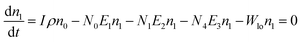
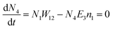
Another possible mechanism is that an enhancement of the local incident electric field leads to the population of the excited levels of Er3+. For understanding this UC emission enhancement mechanism, the rate equations were considered by the energy levels diagram shown in Fig. 5.
| |
 | (1) |
| |
 | (2) |
| |
 | (3) |
| |
 | (4) |
| |
 | (5) |
where the
n0 and
n1 is the population of ground state and excitation state of Yb
3+. The
E1,
E2, and
E3 are the energy transfer from the Yb
3+ to the Er
3+, respectively, as shown in
Fig. 5. The
N0,
N1,
N2,
N3,
N4 denoted the population of ground state (
4I
15/2) and excitation state (
4I
11/2,
4F
9/2,
4S
3/2,
2H
11/2,
4F
7/2,
4I
13/2) of Er
3+, respectively. The
Wl1 and
Wl2 indicates the nonradiative transition from upper energy level (
4S
3/2,
2H
11/2,
4F
7/2,
4I
11/2) to lower energy lever (
4F
9/2,
4I
13/2) of Er
3+, respectively. The
W1,
W2 and
W3 are the radiative transition from the luminescent levels (
2H
11/2,
4S
3/2,
4F
9/2) to ground state (
4I
15/2) of Er
3+, respectively. The
I and
ρ are the excitation field intensity and absorption section, respectively. The
Wl0 is the radiative transition from excitation state (
2F
5/2) to ground state (
2F
7/2) of Yb
3+, which can be neglected. By resolving the rate equations, the population of the luminescent levels of Er
3+ ions can be expressed as:
| |
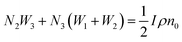 | (6) |
In the eqn (6), the N2W3 and N3(W1 + W2) is the green (Igreen) and red (Ired) UC emission intensity, respectively. Therefore it can be expressed as:
| |
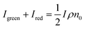 | (7) |
As shown in the eqn (7), the green and red UC emission intensities of the NaYF4:Yb3+, Er3+ nanoparticles is associated with the intensity of excitation field. The strong localized electric field can be created around the APS-1 and APS-2 Au films due to its surface plasmon from Au films, which could result in the enhancement of the excitation field. Thus UC emission of the NaYF4:Yb3+, Er3+ nanoparticles on the APS-1 and APS-2 Au films was enhanced. The electric field intensities and distributions of the APS-1 and APS-2 Au films were simulated, respectively. Based on the SEM image shown in Fig. 2, the size of Au particles and their distance were set as 200 and 100 nm in the ASP-1 Au film, respectively. The thickness of Au films and size of the papilla Au particles were set as 100 nm and 100 nm in the ASP-2 Au film, respectively, and the distance between the papilla Au particles were set as 100 nm. The models of simulated electric field distributions of the ASP-1 and ASP-2 Au film were exhibited in the Fig. 8.
 |
| | Fig. 8 The model of simulated electric field distributions of the ASP-1 and ASP-2 Au film. | |
Fig. 9(a) and (b) exhibited the simulated electric field intensities and distributions of the APS-1 and APS-2 Au films, respectively. As shown in the Fig. 9, the electric field intensities of both Au films were improved, which may result in the UC emission enhancement of the NaYF4:Yb3+, Er3+ nanoparticles. In particular, significant enhancement for the green and red UC emissions of NaYF4:Yb3+, Er3+ nanoparticles deposited on the surface of APS-2 Au film was obtained in contrast to that of APS-1 Au films, which is attributed to the strong enhancement of the local incident electromagnetic field caused by the APS-2 Au film, as shown in Fig. 9. The LSP peak of APS-2 Au film extends from visible to near infrared regions, which is overlapped with the excited light of 980 nm, resulting in well coupling together between the LSP of APS-2 Au film and the excitation light, as shown in Fig. 5. Thus significant excitation enhancement effect was obtained in the APS-2 Au films, resulting in significant enhancement of UC emission of the NaYF4:Yb3+, Er3+ nanoparticles on the surface of APS-2 Au film.
 |
| | Fig. 9 Simulated electric field distributions of APS-1 and APS-2. | |
4. Conclusions
In this paper, the irregular and random Au particles and continuous Au films with papilla Au nanoparticles were used to enhance the UC emission of NaYF4:Yb3+, Er3+ nanoparticles. The UC emission enhancement factors are highly dependent on the topography of Au films. About 77 and 40-folds enhancement were obtained for the green and red UC emission of NaYF4:Yb3+, Er3+ nanoparticles on the irregular and random Au particles, and about 121 and 78-folds enhancement were obtained for the green and red UC emission NaYF4:Yb3+, Er3+ nanoparticles on the continuous Au films with papilla Au nanoparticles, respectively, which were from the increasing of radiative decays rate and significant enhancement of the local electromagnetic field.
Acknowledgements
This work was supported by the Reserve talents project of Yunnan Province (2013HB068), Applied Basic Research Program of Yunnan Province (2014FB127) and Talent Youth Science Foundation of College of materials science and technology (20140205), Kunming University of Science and Technology.
Notes and references
- D. T. Tu, L. Q. Liu, Q. Ju, Y. S. Liu, H. M. Zhu, R. F. Li and X. Y. Chen, Angew. Chem., Int. Ed., 2011, 123, 6430–6434 CrossRef.
- J. Zhou, Z. Liu and F. Li, Chem. Soc. Rev., 2012, 41, 1323 RSC.
- Y. S. Liu, D. T. Tu and H. M. Zhu, Adv. Mater., 2010, 22, 3266 CrossRef CAS PubMed.
- P. Alivisatos, Nat. Biotechnol., 2004, 22, 47–52 CrossRef CAS PubMed.
- X. Xu, M. Li, Y. Xiang, Q. Wang, F. Tang, Y. Wu, Z. Cao and W. Li, Biomaterials, 2010, 31, 8724 CrossRef PubMed.
- Z. Chen, H. Chen, H. Hu, M. Yu, F. Li, Q. Zhang, Z. Zhou and C. Huang, J. Am. Chem. Soc., 2008, 130, 3023 CrossRef CAS PubMed.
- X. Huang, S. Han, W. Huang and X. Liu, Chem. Soc. Rev., 2013, 42, 173 RSC.
- L. M. Yao, J. Zhou, J. L. Liu, W. Feng and F. Y. Li, Adv. Funct. Mater., 2012, 22, 2667 CrossRef CAS.
- F. Wang, J. Wang and X. G. Liu, Angew. Chem., Int. Ed., 2010, 49, 7456–7460 CrossRef CAS PubMed.
- J. C. Boyer and F. C. J. M. van Veggel, Nanoscale, 2010, 2, 1417–1419 RSC.
- S. Schietinger, T. Aichele, H. Q. Wang, T. Nann and O. Benson, Nano Lett., 2010, 10, 134 CrossRef CAS PubMed.
- F. Wang, R. R. Deng, J. Wang, Q. X. Wang, Y. Han, H. M. Zhu, X. Y. Chen and X. G. Liu, Nat. Mater., 2011, 10, 968–973 CrossRef CAS PubMed.
- C. Tao, W. Zhu, Q. An, H. Yang, W. Li, C. Lin, F. Yang and G. Li, J. Phys. Chem. C, 2011, 115, 20053 CAS.
- F. Zhang, G. B. Braun, Y. F. Shi, Y. C. Zhang, X. H. Sun, N. O. Reich, D. Y. Zhao and G. Stucky, J. Am. Chem. Soc., 2010, 132, 2850–2851 CrossRef CAS PubMed.
- H. Zhang, Y. J. Li, I. A. Ivanov, Y. Q. Qu, Y. Huang and X. F. Duan, Angew. Chem., Int. Ed., 2010, 49, 2865–2868 CrossRef CAS PubMed.
- T. Hayakawa, S. T. Selvan and M. Nogami, Appl. Phys. Lett., 1999, 74, 1513–1515 CrossRef CAS.
- W. Feng, L. D. Sun and C. H. Yan, Chem. Commun., 2009, 4393–4395 RSC.
- H. Zhang, D. Xu, Y. Huang and X. F. Duan, Chem. Commun., 2011, 47, 979–981 RSC.
- Y. Chen, K. Munechika and D. S. Ginger, Nano Lett., 2007, 7, 690–696 CrossRef CAS PubMed.
- H. Zhang, Y. J. Li, I. A. Ivanov, Y. Q. Qu, Y. Huang and X. F. Duan, Angew. Chem., Int. Ed., 2010, 49, 2865–2868 CrossRef CAS PubMed.
- T. Ming, H. J. Chen, R. B. Jiang, Q. Li and J. F. Wang, J. Phys. Chem. Lett., 2012, 3, 191–202 CrossRef CAS.
- P. Anger, P. Bharadwaj and L. Novotny, Phys. Rev. Lett., 2006, 96, 113002 CrossRef PubMed.
- P. Jiang, J. F. Bertone, K. S. Hwang and V. L. Colvin, Chem. Mater., 1999, 11, 2132–2140 CrossRef CAS.
- X. Wang, J. Zhuang, Q. Peng and Y. D. Li, Nature, 2005, 437, 121–124 CrossRef CAS PubMed.
- X. Liang, X. Wang, J. Zhuang, Q. Peng and Y. D. Li, Adv. Funct. Mater., 2007, 17, 2757–2765 CrossRef CAS.
- G. S. Yi and G. M. Chow, Chem. Mater., 2007, 19, 341–343 CrossRef CAS.
- M. Wang, J. L. Liu, Y. X. Zhang, W. Hou, X. L. Wu and S. K. Xu, Mater. Lett., 2009, 63, 325–327 CrossRef CAS.
- Y. G. Su, L. P. Li and G. S. Li, Cryst. Growth Des., 2008, 8, 2678–2683 CAS.
- Y. Wang, L. W. Liu, S. Y. Hu, Q. Y. Li, Z. H. Sun, X. H. Miao, X. C. Yang and X. H. Zhang, Acta Phys. Sin., 2013, 19, 197803 Search PubMed.
- W. Xu, Y. S. Zhu, X. Chen, J. Wang, L. Tao, S. Xu, T. Liu and H. W. Song, Nano Res., 2013, 6(11), 795–807 CrossRef CAS.
- W. H. Zhang, F. Ding and S. Y. Chou, Adv. Mater., 2012, 24, op236 CAS.
- G. M. Chen, S. H. Liu, S. J. Chen and Z. N. Qi, Macromol. Chem. Phys., 2001, 202, 1189–1193 CrossRef CAS.
- X. D. Yu, L. Shi, D. Z. Han, J. Zi and P. V. Braun, Adv. Funct. Mater., 2010, 20, 1910–1916 CrossRef CAS.
- P. Y. Yuan, Y. H. Li, M. K. Gnanasammandhan, Z. P. Guan, Y. Zhang and Q. H. Xu, Nanoscale, 2012, 4, 5132 RSC.
|
| This journal is © The Royal Society of Chemistry 2016 |
Click here to see how this site uses Cookies. View our privacy policy here. 


