Hydrogen-terminated mesoporous silicon monoliths with huge surface area as alternative Si-based visible light-active photocatalysts

Ting Lia, Jun Lib, Qiang Zhangb, Emma Blazebya, Congxiao Shangc, Hualong Xud, Xixiang Zhang*b and Yimin Chao*a
aSchool of Chemistry, University of East Anglia, Norwich Research Park, Norwich, NR4 7TJ, UK. E-mail: y.chao@uea.ac.uk
bKing Abdullah University of Science and Technology (KAUST), Division of Physical Science and Engineering, Thuwal 23955, Saudi Arabia. E-mail: xixiang.zhang@kaust.edu.sa
cSchool of Environmental Sciences, University of East Anglia, Norwich, NR4 7TJ, UK
dDepartment of Chemistry, Shanghai Key Laboratory of Molecular Catalysis and Innovative Materials and Laboratory of Advanced Materials, Fudan University, Shanghai 200433, P. R. China

Received 12th April 2016 , Accepted 14th July 2016

First published on 21st July 2016


Abstract

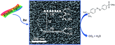
Silicon-based nanostructures and their related composites have drawn tremendous research interest in solar energy storage and conversion. Mesoporous silicon with a huge surface area of 400–900 m2 g−1 developed by electrochemical etching exhibits excellent photocatalytic ability and stability after 10 cycles in degrading methyl orange under visible light irradiation, owing to its unique mesoporous network, abundant surface hydrides and efficient light harvesting. This work showcases the profound effects of surface area, crystallinity, pore topology on charge migration/recombination and mass transportation. Therein the ordered 1D channel array has outperformed the interconnected 3D porous network by greatly accelerating the mass diffusion and enhancing the accessibility of the active sites on the extensive surfaces.


1 Introduction

As it is free and abundant, the use of sunlight to store, transfer and convert energies offers great potential to address some of the most concerned fundamental issues in the sustainable development of human society, future clean fuel schemes, and equally important environmental protection. Significant efforts have been dedicated to explore novel materials and advanced technologies to harness the renewable solar energy as desired.1 Inspired by Nature's photosynthesis, the majority of the research attention has been focused on the development of effective nanomaterials in driving various photochemical reactions in the ultraviolet-visible range of irradiation.2,3 In spite of the remarkable progress that has been made, major setbacks, including narrow light responsive range, wide electronic bandgap, fast charge recombination, and cost ineffective materials, are still challenges facing the search for visible light-active photocatalysts with feasible up-scalability and environmental friendliness.4

Recently, as a promising metal free elemental semiconductor, silicon has received great attention owing to its high activity, natural abundance, low cost, and huge availabilities of Si microelectronic industry infrastructures.5–7 To date, among a range of emerging nano-engineered silicon structures, various efforts have been dedicated to silicon quantum dots (Si QDs) and silicon nanowires (Si NWs) featured by a broad absorption over entire spectral range and tunable bandgap energy.8–14 The photocatalytic potentiality of Si QDs, Si NWs and related composites in CO2 reduction, dye degradation, and selective oxidation has been very well covered in literature.8,9,15

As an indispensable member of the silicon family, porous silicon has been extensively investigated in applications ranging from optoelectronics to emerging fields like sensing,16 battery,17 drug delivery,18,19 and bio-imaging,20,21 since its first discovery in the mid-1950s by Uhlir at Bell laboratory.22 The importance of porous silicon didn't get fully unveiled until 1990s when Canham, Gösele and Lehmann reported the visible photoluminescence at room temperature from porous silicon caused by quantum confinement effect.23,24

The photoactivity of nanoporous silicon in separating the photoexcited e/h+ pairs has been verified, while the promising uses of the sensitive photo-responsivity in solar water splitting, visible light-driven photodegradation of methyl orange, phenol, nitroaromatics have also been broadly discussed.25–28 However, the specific surface area (SSA) is often in the range of 25–300 m2 g−1. Inspired by a recent finding that significant SSA up to 864 and 1125 m2 g−1 has been realized for the first time on p-type porous silicon by electrochemical etching,29,30 mesoporous silicon with large surface area has thus been investigated in this study. To the best of our knowledge, their potential use in photo chemical conversion has yet been evaluated. From practical point of view, porous silicon monoliths can be separated from reaction systems more readily. Its possible scalability, processability, and compatibility with MEMS infrastructure can open up more opportunities in real life use. Compared to the overwhelming amount of work addressed to Si QDs and NWs, the photocatalytic potentiality of porous silicon is still waiting for more exploration and establishing a better understanding of the structural effects is timely required.

Unlike the low dimensional silicon nanomaterials, porous silicon has more complex primary and secondary structural features. For porous materials, the exposed surface and pores govern the reaction kinetics profoundly by adjusting the absorption and loading capacity. Abundant viable active sites on the surface are crucial for surface initiated photochemical conversions, through increasing the surface/volume ratio. Various pore properties (size, length, orderity) also play a critical role in determining the mass transfer. While for porous silicon materials, the microstructural figures embedded on the porous framework also remarkably define its electronic band structure and affect the photo-excited charge carrier generation, recombination. Thus a clearer picture of these multiple morphological factors would be highly valued as more insightful guidance can be gained in rationally designing efficient porous Si materials.

Electrochemical etching is a classic top-down method of producing porous silicon with various topologies.31 The structural properties, such as pore size, pore straightness and surface area, are adjustable with relative ease by simply altering etching parameters (current density, etching time), or using commercially available silicon wafers doped at different levels etc. Therefore it's very favourable to produce porous silicon more controllably with better crystallinity and less defects, which would increase the lifetime of photoexcited electrons/holes that are important to trigger the photocatalytic reaction.32

Given the above background, the aim of this study is to investigate the photocatalytic activity of hydrogen terminated mesoporous silicon (MPSi) with huge surface area prepared by galvanostatic anodization. By analysing the etching-induced surface, pores and microstructures, they are classified into two representative structure models: interconnected 3D network (I-MPSi) and ordered 1D channel array (O-MPSi). Each pros and cons in photocatalysis due to varied structure-related properties are discussed correspondingly with possible solutions to address these limitations for efficiency optimization.

2 Experimental

2.1 Materials

Silicon wafers (moderately boron-doped p-Si (100) chip with a resistivity of 1–10 Ω cm, single side polished, backside etched, Compart Technology, Peterborough, U.K.; heavily boron-doped p-Si (100) chip with a resistivity of 0.001–0.01 Ω cm, single side polished, backside etched, Virginia semiconductor, USA), ethanol (≥99.8%, Sigma-Aldrich), acetone (≥99.5%, Sigma-Aldrich), hydrofluoric acid (48–51 wt% in water, Acros Organics), methyl orange (C14H14N3NaO3S, Fluka Analytical), distilled water.

2.2 Electrochemical etching of silicon

Samples were prepared by electrochemical anodic etching of boron-doped p-Si (100) chip in ethanoic hydrofluoric acid consisting of 48–51% HF aqueous solution and ethanol with a volume ratio of 1[thin space (1/6-em)]:[thin space (1/6-em)]1 at 298 K. Silicon pieces were firstly degreased by ethanol and then transferred to dilute HF/ethanol solution at room temperature to dissolve surface oxides before etching. Then it was sealed into a leak-free Teflon cell, which has a two-electrode configuration. The unpolished side of the silicon chip was attached with a platinum plate and a tungsten coil as current collectors to ensure a homogeneous current distribution on the Si anode. Meanwhile a platinum wire was utilized as the counter electrode to provide a constant etching current generated by Keithley SourceMeter 2601. Immediately after etching terminated, the freshly made sample was carefully removed from the electrolyte to a clean Schlenk flask and dried under vacuum until liquid residue was removed completely so to prevent undesired structural and compositional modification. All samples were carefully handled and stored under nitrogen for next use. The corresponding etching conditions are summarized in Table 1.
Table 1 Etching conditions and textural properties of porous silicon samplesa
MPSi samples I/mA cm−2 t/min Thickness/μm SBET/m2 g−1 Vmeso/cm3 g−1 d/nm
a SBET: multi point BET surface area; Vmeso: mesopore volume; d: mean pore diameter.
I-MPSi-10 10 15 5.8 887.1 1.09 3.07
I-MPSi-30 30 15 20.7 907.0 1.04 3.43
I-MPSi-60 60 15 23.7 994.4 1.36 3.82
I-MPSi-60-05 60 05 14.0 819.2 1.08 3.84
O-MPSi-150 150 05 34.0 458.5 1.76 9.55
O-MPSi-150-10 150 10 58.7 455.3 1.72 9.55


2.3 Sample characterization

The morphology of porous silicon materials were studied by Field Emission Scanning Electron Microscope (FE-SEM) on FEI Helios Nanolab 400S and the applied e-beam voltage was 5 kV; the bright-field images, diffraction patterns and high-resolution TEM (HRTEM) images were all acquired by FEI Titan 80–300 microscope equipped with a high-brightness Schottky-field emission electron source which worked at 300 kV. X-ray powder diffraction (XRD) patterns were recorded by Thermo ARL Xtra diffractometer with Cu Kα radiation (λ = 1.540 Å) at 45 kV and 40 mA to identify the crystalline phase. All scans were made in a 2θ range of 30–80° with a step size of 0.01° and a step time of 1 s using aluminium sample holders. The chemical composition of porous silicon was distinguished by Attenuated Total Reflectance (ATR) Fourier Transform-Infrared (FT-IR) Spectroscopy (PerkinElmer Spectrum 400) and each spectrum was averaged over 32 scans with a resolution of 4 cm−1. The optical properties were characterized by UV-vis spectrometer (Perkin Elmer Lambda 35) and fluorescence spectrometer (Perkin-Elmer LS55). The nitrogen sorption isotherms were performed on Quantachrome Autosorb-1 instrument at 77 K. All samples were degassed below 473 K for 3 h before the measurements were carried out. The specific surface area (SSA) was derived from the adsorption isotherm via the application of Brunauer–Emmett–Teller (BET) theory in the domain of relative pressure between 0.05 and 0.3. The micropore analysis was performed using t-plot method. The pore size distribution was measured by the Barrett–Joyner–Halenda (BJH) approach. The total pore volume was obtained from the amount adsorbed at relative pressure P/P0 = 0.99.

2.4 Photocatalytic activity

Methyl orange (MO) degradation under visible light irradiation was employed to evaluate the photocatalytic activity of our samples. An 8 W fluorescent lamp was employed as the visible light source and glass vials were used in the experiments to filter out ultraviolet irradiation. The reactions were carried out in a 15 mL glass vial, containing 2 mg MPSi thin layer (disk-like, the diameter is 1.1 cm and the external surface area is 1.9 cm2) and 4 mL MO solution with initial concentration of 5.0 × 10⁻⁵ M under stirring. The remaining MO concentration was measured by monitoring the absorption peak at λmax = 464 nm using UV-vis absorption spectrometer (Perkin Elmer Lambda 35). All experiments were carried out under ambient conditions at room temperature. The organic carbon content in liquid samples was detected by Skalar Total Organic Carbon Analyser (TOC). For the cycle runs, MPSi was simply washed with 5 wt% aqueous HF prior to the next cycle.

3 Results and discussion

3.1 Characterization of mesoporous silicon thin films

I-MPSi-30 and O-MPSi-150 have been characterized as the respective representatives for typical I-MPSi and O-MPSi structures. Their distinct microscopic morphologies are clearly illustrated in Fig. 1. As presented, both silicon substrates are significantly porosified along with the formation of numerous pores with narrow interspacings after etching. This is well known as two-electron electrochemical reaction, resulting in the silicon atoms rapidly dissolving into soluble substances in HF solution under anodic polarization.33 More specifically I-MPSi-30 (Fig. 1A) shows much smaller pores (4.7 nm, Fig. 1E) and thinner pore walls than O-MPSi-150 (Fig. 1B) of which the average pore size is measured to be 10.5 nm, seen in the PSD curve (Fig. 1F). As shown in Fig. 1A and B insets, the porous layer thickness is 20.7 μm and 34.0 μm respectively and it is considerably consistent for the entire layer (Fig. S1). The cross-section images for I-MPSi-30 and O-MPSi-150 are characterized in Fig. 1C and D. A nicely ordered 1D channel array is shown in O-MPSi-150 with nanoscale silicon filaments homogeneously developed on the pore walls. The pores are parallel to each other and perpendicular to the substrate, propagating in the [100] direction primarily (Fig. S2). On the contrary, I-MPSi-30 is seen as a highly interconnected 3D porous network while the general top-down texturing is still observable (Fig. S2). As presented in the high magnification Fig. 1C inset, the silicon matrix is also densely embedded with massive irregular Si nanocrystals.
image file: c6ra09474k-f1.tif
Fig. 1 FE-SEM images of as etched I-MPSi-30 ((A) top view; (C) cross-section) and O-MPSi-150 ((B) top view; (D) cross-section). Inset (A and B) layer thickness; inset (C and D) higher magnification cross sectional images. Histograms of pore size distribution of I-MPSi-30 (E) and O-MPSi-150 (F) derived from FESEM micrographs; X-ray diffraction patterns (G) and ATR-IR spectra (H) of I-MPSi-10 (a), I-MPSi-30 (b), I-MPSi-60 (c) and O-MPSi-150 (d).

X-ray diffraction analysis in Fig. 1G reveals a preserved crystallinity throughout the highly eroded frameworks, showing a strong peak centered at 2θ between 69.0° and 69.2°, attributable to crystal plane (400) of silicon. Various degrees of broadening in full width at half maximum (FWHM) represent the existence of nanocrystallites with different sizes constituting the macroscopic lattice. Based on the individual peak profile, Si particle size is calculated to be 11.2 nm, 7.1 nm, 5.5 nm and 17.3 nm for I-MPSi-10, I-MPSi-30, I-MPSi-60 and O-MPSi-150, respectively, according to Scherrer equation. Notably the nanocrystal size reduces with higher etching current density and I-MPSi samples possess much finer microstructures than O-MPSi-150 in agreement with the FESEM observation. According to pore-forming mechanisms, these nano-features are formed as a result of electrochemical etching, chemical dissolution, and quantum confinement effect.33,34 As smallest regions of porous framework, they play a key role in achieving a high surface area on porous silicon, and also can alter the optical properties profoundly.

Fig. 1H displays the ATR-IR spectra of I-MPSi-10 (a), I-MPSi-30 (b), I-MPSi-60 (c) and O-MPSi-150 (d). Six characteristic peaks are presented in each spectrum with the strongest Si–Si band at 615 cm−1. The absorptions at 664 cm−1 and 910 cm−1 are originated from Si–H wagging and scissoring modes, revealing the intense etching that occurred on the surface. The fact is further confirmed by the presence of peaks at 2087 cm−1, 2110 cm−1, 2139 cm−1, commonly assigned to the stretching modes of SiHx species (x = 1, 2, 3, respectively) on the surface. Since there is neither Si–O stretching peak in the range of 1000–1200 cm−1 nor any absorption around 2260 cm−1, corresponding to SiOySiHx (x + y = 4, x = 1, 2, 3) complexes in all spectra, it has shown that the as-etched surface is free of oxide phases and purely hydrogen terminated. In fact the surface species especially Si–H bonds appear to be very crucial in determining the photoactivity of silicon nanomaterials.9,12,35 In that sense the abundant hydrides generated on the surfaces of I-MPSi and O-MPSi samples can be expected to promote the photocatalytic performance.

A nitrogen physisorption analysis has been carried out for a more precise examination of their structural characteristics. Quantitative results are summarized in Table 1. The adsorption/desorption isotherms of nitrogen onto I-MPSi samples (I-MPSi-30 in Fig. 2A and others in Fig. S3) exhibit typical type-IV curves with distinct capillary condensation step at P/P0 ∼ 0.4, which is featured by a H2 hysteresis loop. Multi point BET analysis of the adsorption isotherm of I-MPSi-30 yields an exceptionally high surface area up to 907.0 m2 g−1. The average pore diameter is 3.43 nm derived from the adsorption branch using BJH model. The total mesopore volume is 1.04 cm3 g−1. The SSA can further reach up to almost 1000 m2 g−1 by increasing the current density to 60 mA cm−2. According to the results in Table 1, not only SSA, but pore volume and pore size are also increased with higher etching current density along with a broader pore size distribution (Fig. 2B). However the increasing surface tension arose from severely etched porous structure under high etching current density also tends to impair the mechanical stability of the MPSi monoliths. Thus additional techniques, such as super critical drying, are essential to tackle this issue so more prominent SSA is achievable on I-MPSi.29,30


image file: c6ra09474k-f2.tif
Fig. 2 Nitrogen sorption isotherms (A) of I-MPSi-30 (a) and O-MPSi-150 (b); pore size distribution (B) of I-MPSi-30 (a), O-MPSi-150 (b), I-MPSi-10 (c) and I-MPSi-60 (d) acquired by BJH approach.

In the IV-H1 type isotherms of O-MPSi samples (O-MPSi-150 in Fig. 2A and others in Fig. S3), the capillary condensation has occurred at a higher relative pressure of 0.7, demonstrating the existence of much larger pores than I-MPSi samples. The average pore size for O-MPSi-150 is extracted as 9.55 nm, which is in good accordance with the FESEM observation (10.5 nm) and HRTEM data (9.4 nm) in Fig. 3. In contrast with I-MPSi which has a larger surface area, the larger pore size and pore volume is unique for O-MPSi samples.


image file: c6ra09474k-f3.tif
Fig. 3 HRTEM images and SAED patterns of I-MPSi-30 (A–C) and O-MPSi-150 (D–F).

HRTEM examination of the pore qualities such as regularity, interconnectivity, crystallinity has also performed. As presented in Fig. 3, abundant pores have been formed. In agreement with the previous FESEM findings, the highly interconnected porous network is featured in I-MPSi-30, while the nicely aligned 1D channel arrays are spotted in O-MPSi-150. One can see rough surface from both samples. Selected area electron diffraction (SAED) analysis (B and E) has been performed to identify the lattice configuration. Patterns from I-MPSi-30 (B) and O-MPSi-150 (E) have shown diffraction spots corresponding to (400), (220), (111) planes of the diamond cubic structure. In contrast to the well-defined monocrystalline structure of O-MPSi-150, the pattern from I-MPSi-30 exhibits slight deviation, which can be explained by the increased surface stresses resulted from the high SSA up to 907.0 m2 g−1 and finite 5.8 nm Si nanoparticles by the intense cavitation. Nevertheless, the lattice fringes with 0.313 nm inter-planar spacing of Si (111) plane is still observable (Fig. 3C inset).

The optical properties of porous samples have been investigated by means of UV-vis absorption and emission spectroscopies. As seen in Fig. 4A, the absorption spectra of I-MPSi-30 (a) and O-MPSi-150 (b) span across a very broad region from 250 nm to 800 nm, as a result of an enlarged bandgap between the conductive and valence bands due to quantum confinement effect. Therefore, more photons can be absorbed and more visible light energy can be utilized. In addition to the widened bandgap, the light harvesting can further be strengthened by the rough textures of the vast surface suppressing the light reflection at the interface. The peak position for I-MPSi-30 is at 254 nm, which is at shorter wavelength than that from O-MPSi-150 in regard to the smaller Si nanocrystals contained in the structure. Despite the differences in the morphology possessed by I-MPSi and O-MPSi samples, they have shown similar absorption ability in the visible light range.


image file: c6ra09474k-f4.tif
Fig. 4 UV-vis absorption (A) and PL emission spectra (B) (excitation wavelength = 320 nm; 390 nm cutoff) of freshly made I-MPSi-30 (a), O-MPSi-150 (b) and partially oxidized I-MPSi- 30 (c); UV-vis absorption of methyl orange (MO) solution before and after adding I-MPSi-30 (C and D) and O-MPSi-150 (E and F) as a function of degradation time. (C) and (E) were subjected to the visible light irradiation (λ > 400 nm); (D) and (F) were performed in the absence of light. The initial concentration of MO is 5.0 × 10⁻⁵ M. The lamp power = 8 W.

Another concerning optical factor is the recombination of photo-excited charges. Multiple emission bands are shown in Fig. 4B featured by the main peak at 460 nm for I-MPSi-30 and 474 nm for O-MPSi-150. It's well acknowledged that the low fluorescence intensity represents a high separation efficiency of electron–hole pairs. The emission intensity from O-MPSi-150 is even lower than that from I-MPSi-30. The better charge transfer ability can be ascribed to several structural superiorities. Firstly the intrinsic lower resistivity of the parental wafer for O-MPSi sample provides a better electrical conductivity across the surface. The better lattice integrity of O-MPSi-150 also enhances the migration of free charges by providing less surface defects and higher resistance to the oxidation. On the contrary, the red emission at 609 nm is presented in the spectrum of I-MPSi-30, which is often recognized as a result of surface oxidation and it is also affirmed in the experiment here since the signal is clearly intensified after purposely oxidizing the sample (Fig. 4Bc). The vulnerability of I-MPSi sample to surface oxidation is likely due to its ultra-huge specific surface area. Meanwhile its poorer crystallinity and detectable lattice distortion may also cause more structural defects. In fact the formed oxides and existing defects are widely reported to be involved in the radiative recombination of photo-excited charge carriers.32,36

3.2 Photocatalytic activities

In order to investigate the structural effect on decomposition of methyl orange (MO), the photocatalytic behaviours of mesoporous silicon with different morphologies have been studied under visible light irradiation. Fig. 4C and E showed the variation of peak absorbance of MO at 464 nm against the degradation time in the presence of I-MPSi-30 and O-MPSi-150 under visible light irradiation respectively. Likewise, Fig. 4D and F showed the same correlations of MO absorbance and reaction time for the unirradiated counterparts. It's clear to see for different samples under different illumination conditions, the 464 nm peak all reduced in intensity but at different rates. For a more comprehensive comparison, the concentration ratios of unreacted MO molecules derived from the UV-vis absorption data are plotted against the decomposition time in Fig. 5 for all the samples. As displayed, MO self-degradation is almost negligible and no MO degradation has been observed in any of the control experiments (Fig. S4). The first-order rate constant (k, h−1) and photocatalytic efficiency (η, %) of each sample are listed in Table 2.
image file: c6ra09474k-f5.tif
Fig. 5 The MO degradation rates for I-MPSi-30 (light on: closed circle; light off: open circle), O-MPSi-150 (light on: closed up triangle; light off: open up triangle), O-MPSi-200 (light on: closed down triangle) and sonicated I-MPSi-30, O-MPSi-200. Photolysis of methyl orange solution was also plotted as reference (square). More control experiments can be found in Fig. S4.
Table 2 The reaction kinetics of MPSi samples
MPSi samples Rate constant (k)/h−1 Photocatalytic efficiency (η)a/%
a Photocatalytic efficiency (η): the concentration ratio of decomposed organics when the reaction proceeded for 60 min.
I-MPSi-30 dark 0.22 13.7
I-MPSi-30 0.39 23.7
O-MPSi-150 dark 0.48 40.0
O-MPSi-150 0.86 53.9
O-MPSi-200 1.98 89.7
I-MPSi-30-S 0.68 40.0
O-MPSi-200-S 2.31 99.8


Both I-MPSi and O-MPSi samples show an obvious reactivity towards MO even under dark conditions. The rate constant is calculated to be 0.22 h−1 for I-MPSi-30, and 0.48 h−1 for O-MPSi-150. This is related with the characteristic aspects of the mesoporous silicon monolith, such as large internal surface area, open mesopores, abundant active hydrides that are demonstrated in Fig. 1H and become accessible to the organic substances.

Take I-MPSi-30 as an example, the evolvement of the surface species during the reaction has been monitored by the IR spectra of porous silicon at different intervals. As shown in Fig. S5, the surface hydrides are consumed significantly accompanied by the intensified Si–O–Si stretching band centered at 1067 cm−1 as the reaction time increased from 0 min to 360 min. As reported in literature, the C–N bond between the aromatic ring and azo bond for MO is easy to rupture by reductive bonds.13 Thus silicon hydrides can chemically react with MO molecules by hydrogen transfer which often lies behind its widely exploited surface modification via hydrosilylation with various ligands. Additionally the structural strain is likely to enhance the reactivity of the Si–Hx functional groups on the rough surfaces as well.

In order to further illustrate, Fig. S6 shows the results after the hydrides on the surfaces of I-MPSi-30 and O-MPSi-150 are totally quenched by dilute hydrogen peroxide solution resulting in the pore walls covered by a thin layer of silicon oxides. UV-vis absorption measurement shows degradation of MO is not detectable, which experimentally confirms the organic molecules are decomposed irreversibly by silicon hydrides owned by porous silicon. In fact it takes more time for I-MPSi-30 to oxidize the entire surface than O-MPSi-150, which also implies the larger surface area and more hydrides species it possesses. The as-described reduction ability of H-terminated porous silicon is an interesting topic and I-MPSi/O-MPSi samples in this study have presented their potentiality as efficient reducing agent for various applications.

Owing to the nature of the active H-terminated surface of porous silicon, the physical absorption–desorption equilibrium for the dye is unlikely to be achieved within the structure of H-terminated mesoporous silicon without any MO being chemically converted. Nevertheless, by measuring the amount of MO molecules absorbed by the partially oxidized samples, one can clearly see that the physisorption is considerably insignificant compared to the reaction rate (Fig. S7 and S8).

Under the light irradiation, the degradation rate constant is 0.39 h−1 for I-MPSi-30, and 0.86 h−1 for O-MPSi-150, respectively, much faster than the respective reaction rate under dark conditions. The excellent light absorption of I-MPSi-30 and O-MPSi-150 has served as an essential prerequisite of their outstanding activity. Taking advantage of the huge surface area, mesoporous network, large pore volume, and H-passivated surfaces, mesoporous silicon samples have showcased their excellent photo-efficiency. By measuring the total organic carbon content in the solution at different intervals during the degradation, one can see that the amount of organics decreased as the irradiation time increased (Fig. S9). For O-MPSi-150, the mass of organic matter decreased by 20% after 120 min irradiation in agreement with the reported photocatalytic decomposition mechanisms of silicon nanostructures in the presence of external illumination.37 In the meantime, the active hydrides also attack the C–N bond of MO molecules, which largely promote the dye decolorization. Thus both pathways facilitate the rapid photocatalytic decomposition of MO under visible light irradiation by mesoporous silicon. While under dark conditions, the hydrogen transfer process plays a main part. Silicon hydrides can not only directly reduce the methyl orange through the hydrogen transfer but they also are reported to be crucial for the photocatalytic activity as well. Thus the roles of silicon hydrides in the photocatalytic decomposition are always a research hot spot for silicon QDs, NWs and porous structures. For example, many researchers have found out the various functionalities of silicon hydrides acting as electron sinks and increasing the average lifetime of photo-excited e/h+ etc.9,12,35 In this study, as described above, the surface hydrides are also very active. Thus the interactions between the hydrides, e/h+, photons and reactants are very complex matter and further exploration is under way for a clearer understanding of this interesting topic.

As revealed above, I-MPSi-30 possesses a much larger SSA than O-MPSi-150, and a large surface area of semiconductors is often known to be favoured for facilitating the photo-induced e/h+ separation and transfer. However this impact for I-MPSi-30 is likely to be compensated by the relatively poor crystallinity and more surface defects acting as e/h+ recombination centers. More importantly, as further evidence showed, the pore topology exerts a great impact on the actual activity of mesoporous silicon monoliths.

In liquid phase reaction system, mass transport is vitally important for heterogeneous photocatalysts and often restricts the catalytic performance. Accessible mesopores can considerably ease the diffusion resistance. As described above, the mean pore size for I-MPSi-30 and O-MPSi-150 are 3.43 nm and 9.55 nm respectively. The severity of diffusion resistance is proportional to the molecular size and inversely to the pore size. Therefore, the larger pore dimension has released the diffusion limitation for O-MPSi sample. In addition, the large pore volume of O-MPSi as 1.76 cm3 g−1 also can increase the reactant payload by absorption and capillary driven infiltration, which is leading to a higher concentration of reactants inside the pores and consequently enhancing the reaction rate. By comparing the physisorption results of aforementioned oxidized samples, O-MPSi-150 does show a faster absorption and larger loading capacity (Fig. S8), although the artificial surface oxidization might slightly shrink the pore diameter of the samples.

With respect to MO and its degradation intermediates in this study, the porous system with 3.43 nm pore diameter and 1.04 cm3 g−1 pore volume is still capable of accommodating the reaction species. Indeed it is another pore property that contributes to the slower reaction rate for I-MPSi-30. As known, mass transportation is also strongly affected by the length in diffusion path. Therefore, the interconnected mesoporous network in I-MPSi samples increases the travel distance for reactants to reach the active surface, while in O-MPSi-150, the vertically aligned ordered pores facilitate the vast internal surface to be more accessible. As a consequence, O-MPSi-150 exhibits a better efficient degradation than I-MPSi-30.

These effects of SSA and pore properties are further reflected in the performance of O-MPSi-200 sample prepared by electrochemical etching in the same manner with current density increased to 200 mA cm−2. It has all the merits in pore topology as O-MPSi-150 but with larger pores and higher SSA. It also achieved an excellent light absorptivity (Fig. S10). As expected it shows an even faster MO degradation rate of which the rate constant is up to 1.98 h−1 (Fig. S11).

The influences of pore straightness or interconnectivity are also reflected in the various accelerations for I-MPSi-30 and O-MPSi-200 gained by a simple sonication post-treatment. After lifting the mesoporous silicon layer off the supported Si chip, it has been sonicated into microparticles in DCM under nitrogen gas flow. The IR spectra shows the hydrogen passivated surfaces are still retained and no silica formed (Fig. S12). As a result, the pore length is reduced and the internal surface area is more exposed to reactants so diffusing into the porous system becomes more readily. As expected, the reaction progress has been enhanced prominently by 73% for I-MPSi sample, and 17% for O-MPSi sample (Fig. S13). This is because the diffusion barrier caused by the intrinsic pore topology for I-MPSi-30 has been effectively reduced through mechanical force-induced structure modification.

Last but not the least, the catalyst lifetime of mesoporous silicon monoliths is also evaluated. O-MPSi-200 is selected as it presents the best activity among all samples. As shown in Fig. 6, the efficiency slightly decreases as the number of cycles goes up, but 88% of the 1st cycle activity has still been maintained extraordinarily even after 10 cycles.


image file: c6ra09474k-f6.tif
Fig. 6 The cycle runs of O-MPSi-200.

4 Conclusions

From the perspectives of catalyst designing and structural optimization, the photocatalytic behaviours of hydrogen terminated mesoporous silicon have been investigated. A broad light absorption and efficient charge separation have contributed to the promising photocatalytic ability towards methyl orange under visible light irradiation up to 10 cycles, assisted by the large H-passivated surface area, accessible porous system, and abundant finer scale structural figures. The overall performance is a combined effect of structural, optical and electrical properties. By making direct comparison between interconnected porous network and ordered pore arrays, it is discovered that the pore topology imposes a strong impact on the photocatalyst efficacy through regulating the mass transport process which favours larger pore size and better pore straightness. The influences can be effectively altered by adjusting the preparation conditions or developing post-processing methods to release the diffusion barriers for reactants. Above all this study has shed more insights into the structural engineering of porous silicon as a novel visible light-active candidate for driving dye decomposition for environmental remediation. The findings here are applicable to wider fields in rational optimizing the efficiency of porous silicon in solar energy storage and conversion, novel drug delivery systems among others.

Acknowledgements

T. L. is grateful to an International studentship awarded by University of East Anglia.

Notes and references

  1. D. Gust, T. A. Moore and A. L. Moore, Acc. Chem. Res., 2001, 34, 40 CrossRef CAS PubMed.
  2. P. V. Kamat, J. Phys. Chem. C, 2007, 111, 2834 CAS.
  3. S. Linic, P. Christopher and D. B. Ingram, Nat. Mater., 2011, 10, 911 CrossRef CAS PubMed.
  4. X. Xie, K. Kretschmer and G. Wang, Nanoscale, 2015, 7, 13278 RSC.
  5. G. Liu, P. Niu and H. M. Cheng, ChemPhysChem, 2013, 14, 885 CrossRef CAS PubMed.
  6. S. Chandrasekaran, T. Nann and N. H. Voelcker, Nano Energy, 2015, 17, 308 CrossRef CAS.
  7. X. Liu, P. R. Coxon, M. Peters, B. Hoex, J. M. Cole and D. J. Fray, Energy Environ. Sci., 2014, 7, 3223 CAS.
  8. Z. Kang, C. H. Tsang, N. B. Wong, Z. Zhang and S. T. Lee, J. Am. Chem. Soc., 2007, 129, 12090 CrossRef CAS PubMed.
  9. M. Shao, L. Cheng, X. Zhang, D. D. Ma and S. T. Lee, J. Am. Chem. Soc., 2009, 131, 17738 CrossRef CAS PubMed.
  10. Y. Qu, X. Zhong, Y. Li, L. Liao, Y. Huang and X. Duan, J. Mater. Chem., 2010, 20, 3590 RSC.
  11. Z. Kang, Y. Liu and S. T. Lee, Nanoscale, 2011, 3, 777 RSC.
  12. N. Megouda, Y. Cofininier, S. Szunerits, T. Hadjersi, O. Elkechai and R. Boukherroub, Chem. Commun., 2011, 47, 991 RSC.
  13. F. Y. Wang, Q. D. Yang, G. Xu, N. Y. Lei, Y. K. Tsang, N. B. Wong and J. C. Ho, Nanoscale, 2011, 3, 3269 RSC.
  14. R. Liu, G. B. Yuan, C. L. Joe, T. E. Lightburn, K. L. Tan and D. W. Wang, Angew. Chem., Int. Ed., 2012, 51, 6709 CrossRef CAS PubMed.
  15. F. Liao, T. Wang and M. Shao, J. Mater. Sci.: Mater. Electron., 2015, 26, 4722 CrossRef CAS.
  16. M. J. Sailor and E. C. Wu, Adv. Funct. Mater., 2009, 19, 3195 CrossRef CAS.
  17. X. Li, M. Gu, S. Hu, R. Kennard, P. Yan, X. Chen, C. Wang, M. J. Sailor, J. G. Zhang and J. Liu, Nat. Commun., 2014, 5, 4105 CAS.
  18. J. H. Park, L. Gu, G. von Maltzahn, E. Ruoslahti, S. N. Bhatia and M. J. Sailor, Nat. Mater., 2009, 8, 331 CrossRef CAS PubMed.
  19. M. Behray, C. A. Webster, S. Pereira, P. Ghosh, S. Krishnamurthy, W. T. Al-Jamal and Y. Chao, ACS Appl. Mater. Interfaces, 2016, 8, 8908 CAS.
  20. L. Gu, D. J. Hall, Z. Qin, E. Anglin, J. Joo, D. J. Mooney, S. B. Howell and M. J. Sailor, Nat. Commun., 2013, 4, 2326 Search PubMed.
  21. J. H. Ahire, Q. Wang, P. R. Coxon, G. Malhotra, R. Brydson, R. Chen and Y. Chao, ACS Appl. Mater. Interfaces, 2012, 4, 3285 CAS.
  22. A. Uhlir, Bell Syst. Tech. J., 1956, 35, 333 CrossRef CAS.
  23. L. T. Canham, Appl. Phys. Lett., 1990, 57, 1046 CrossRef CAS.
  24. V. Lehmann and U. Gösele, Appl. Phys. Lett., 1991, 58, 856 CrossRef CAS.
  25. J. Su, H. Yu, X. Quan, S. Chen and H. Wang, Appl. Catal., B, 2013, 138–139, 427 CrossRef CAS.
  26. B. H. Meekins, Y. C. Lin, J. S. Manser, K. Manukyan, A. S. Mukasyan, P. V. Kamat and P. J. McGinn, ACS Appl. Mater. Interfaces, 2013, 5, 2943 CAS.
  27. F. Dai, J. Zai, R. Yi, M. L. Gordin, H. Sohn, S. Chen and D. Wang, Nat. Commun., 2014, 5, 3605 Search PubMed.
  28. H. Xu, H. Xiao, H. Pei, J. Cui and W. Hu, Microporous Mesoporous Mater., 2015, 204, 251 CrossRef CAS.
  29. A. Loni, T. Defforge, E. Caffull, G. Gautier and L. T. Canham, Microporous Mesoporous Mater., 2015, 213, 188 CrossRef CAS.
  30. A. Loni, L. T. Canham, T. Defforge and G. Gautier, ECS J. Solid State Sci. Technol., 2015, 4, P289 CrossRef CAS.
  31. L. Canham, Handbook of porous silicon, Springer International Publishing, 2014 Search PubMed.
  32. K. Wang, Q. Wang and Y. Chao, Appl. Phys. A, 2012, 109, 437 CrossRef CAS.
  33. G. X. Zhang, in Modern Aspects of Electrochemistry, Springer, New York, 2006, p. 65 Search PubMed.
  34. H. Föll, M. Christophersen, J. Carstensen and G. Hasse, Mater. Sci. Eng., R, 2002, 39, 93 CrossRef.
  35. D. Liu, L. Li, Y. Gao, C. Wang, J. Jiang and Y. Xiong, Angew. Chem., Int. Ed., 2015, 54, 2980 CrossRef CAS PubMed.
  36. P. R. Coxon, Q. Wang and Y. Chao, J. Phys. D: Appl. Phys., 2011, 44, 495301 CrossRef.
  37. C. Chen, W. Ma and J. Zhao, Chem. Soc. Rev., 2010, 39, 4206 RSC.

Footnote

Electronic supplementary information (ESI) available: Sample details, more SEM images, UV-vis and PL spectra, and IR measurement details. See DOI: 10.1039/c6ra09474k

This journal is © The Royal Society of Chemistry 2016
Click here to see how this site uses Cookies. View our privacy policy here.