Solution-stable anisotropic carbon nanotube/graphene hybrids based on slanted columnar thin films for chemical sensing

Peter M. Wilsona, Adam Zobela, Anita J. Zaitounaa, Alexey Lipatova, Eva Schubertbc, Tino Hofmannbcd, Mathias Schubertbc, Rebecca Laiac and Alexander Sinitskii*ace
aDepartment of Chemistry, University of Nebraska-Lincoln, Lincoln, NE 68588, USA. E-mail: sinitskii@unl.edu; Fax: +1-402-472-9402; Tel: +1-402-617-3543
bDepartment of Electrical Engineering, University of Nebraska-Lincoln, Lincoln, Nebraska 68588, USA
cNebraska Center for Materials and Nanoscience, University of Nebraska-Lincoln, Lincoln, NE 68588, USA
dDepartment of Physics, Chemistry and Biology (IFM), Linköping University, SE 581 83 Linköping, Sweden
eNational University of Science and Technology “MISIS”, Moscow 119991, Russia

Received 10th April 2016 , Accepted 21st June 2016

First published on 23rd June 2016


Abstract

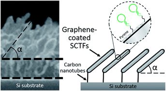
Slanted columnar thin films (SCTFs) are promising anisotropic nanostructures for applications in optical sensing and chemical separation. However, the wide use of SCTFs is significantly limited by their poor mechanical properties and structural stability, especially in liquid media. In this work, we demonstrate the fabrication of solution-stable carbon nanotube (CNT)/graphene hybrid structures based on cobalt SCTFs. The CNT/graphene hybrid structures were synthesized through the use of a titanium underlayer for Co slanted nanopillars as a chemical vapor deposition catalyst, which allows simultaneous growth of CNTs at the Co/Ti interface and three-dimensional graphene over the surface of cobalt. Importantly, the CNT/graphene hybrid structures retain the anisotropy of the parent Co SCTFs and thus remain suitable for optical sensing. Graphene/CNT modification of Co SCTFs not only improves their stability in solutions but also enables their functionalization with pyrene-modified DNA probes, which can be monitored in real time by in situ ellipsometry measurements. In turn, the solution-stable DNA-modified SCTFs may find a wide range of applications in biosensing. The described synthetic approach that allows simultaneous growth of CNTs and graphene by engineering Co/Ti interfaces may also be applied to the fabrication of other kinds of complex CNT/graphene hybrid materials.


Surfaces with self-organized, spatially coherent arrangements of nanostructures have unique optical, mechanical, and electrical properties which differ dramatically from the bulk materials.1–4 The optical and transport properties of sculptured columnar thin films (SCTFs) have attracted recent interest because of their potential to achieve novel optical sensing and separation mechanisms with few femtogram μm−2 sensitivities to chemical adsorption to the nanostructured surface.5–7 The microscopic origin of this remarkable optical sensitivity is the dielectric screening of the anisotropic optical response which is due to the high spatial coherence of electrically insulated arrays of sub-wavelength dipole antennas. However, the optical response is not selective to different analytes, which impairs its usefulness for sensing applications. One way to remedy this is by incorporation of analyte-specific binders which would result in selective enhancement of the signal upon introduction of the target analyte. This can be accomplished by coating the SCTFs with a conformal graphene layer that encapsulates each individual nanopillar. After coating with graphene, well-known functionalization techniques such as diazonium8 or pyrene chemistry9 can be performed allowing the attachment of analyte-specific binders.

Fig. 1a shows the scheme of the resulting sensor platform. It shows an array of slanted nanopillars that are conformally coated with graphene. This coating allows the attachment of a pyrene-modified DNA probe that is immobilized on the surface of graphene via π–π stacking. In the presence of the full-complement target, the DNA stem will be disrupted in favour of the thermodynamically more stable probe–target duplex, which will result in the optically detectable change in dielectric screening of SCTFs. Different varieties of analyte-specific DNA sequences can be potentially attached to graphene-modified SCTFs, enabling a wide range of optical biosensors.


image file: c6ra09252g-f1.tif
Fig. 1 (a) Scheme of an optical sensor platform that comprises graphene-coated SCTFs functionalized with pyrene-modified DNA probes. (b) Photograph of graphene-coated cobalt SCTF. The circular region in the centre was confined by an O-ring and exposed to a solution. (c) Cross-section SEM image of the graphene-coated SCTF that was taken at the untreated region that was protected from solution by an O-ring. (d) Cross-section SEM image of the graphene-coated SCTF that was exposed to a solution.

Our previous research has demonstrated a process whereby metallic SCTFs can be coated with graphene using chemical vapour deposition (CVD).10 However, the described graphene-coated nanopillar sensors are limited by weak structural integrity in solution because the nanopillars interact with the substrate via weak van der Waals interactions making them easily washed away in solution. The destruction of the SCTFs in solution can is illustrated using scanning electron microscopy (SEM). Fig. 1b shows the optical photograph of a silicon substrate, on which graphene-coated Co SCTFs were fabricated. The centre of the substrate was confined by an O-ring, and then exposed to a Phys 2 buffer solution. A cross-section SEM image taken in the area outside the O-ring shows a well-ordered structure of a graphene-coated Co SCTF that was not exposed to a solution (Fig. 1c). However, Fig. 1d shows that in the area inside the O-ring the nanopillars were washed away or collapsed.

In theory, the instability of SCTFs in solution can be counteracted by the extraordinary stability of carbon allotropes. For instance graphene has been shown to have remarkable mechanical strength coupled with high flexibility.11–13 Graphene has also demonstrated chemical inertness to a variety of different chemical treatments, suggesting the ability to protect nanostructures from caustic environments.14–16 More recently, we demonstrated that graphene is capable to stabilize delicate nanostructures, such as SCTFs, at elevated temperatures at which bare nanostructures would suffer damage.17 In light of the previous successes of graphene-coated nanostructures it seems possible that engineering a graphene coating on the SCTFs would not only provide an avenue to impart analyte selectivity but also improve their structural stability to increase the adhesion.

A possible method for increasing the stability of the SCTFs is to alter the morphology of the carbon coating and, rather than using only a conformal graphene component, introduce an interfacial adhesion layer of CNTs to attach the graphene sheets to the surface of the substrate, thereby increasing the strength of the attachment of the nanopillars to the surface. Several studies have been conducted growing CNT/graphene hybrids.18–21 In general, the procedures involved two CVD steps. In the first, a layer of graphene was grown. Afterward, the graphene was seeded with catalytic nanoparticles and a second CVD step would grow CNTs that were covalently attached to the graphene. However, since CNT and graphene growth occur under similar conditions, it is feasible to engineer a catalytic material that will simultaneously grow both CNTs and graphene in predetermined regions. Recently, using a vermiculite–FeMo composite, a CNT/graphene sandwiched structure was obtained by a single CVD procedure in which graphene grew on the vermiculite while the CNTs grew from the FeMo nanoparticles, demonstrating the principle of single-step growth of CNT/graphene hybrids.22

We propose to expand on this concept by engineering the cobalt catalyst makeup resulting in growth of CNTs and graphene at selected regions in a single CVD step. Although cobalt is a well-known catalyst for growth of CNTs,23 under certain conditions it has been shown that CVD will instead result in growth of graphene conformally coating the nanostructures.10 However, previous studies have shown that cobalt/titanium alloys have a higher propensity for CNT growth than either cobalt or titanium.24 It may be possible that deposition of cobalt SCTFs on a titanium thin film will result in CNT growth at the interface of the cobalt and the titanium, due to the mixing of cobalt and titanium and the greater tendency for cobalt/titanium alloys to form CNTs. Thus it may be possible to grow an interfacial layer of CNTs that will stabilize the SCTF structure and anisotropy in solution, making the material viable for implementation as a chemical sensor.

The nanostructured catalyst was fabricated by e-beam deposition of a 30 nm titanium thin film over the surface of p-doped silicon wafer. Glancing angle deposition (GLAD) of cobalt was then conducted as described in previous work.25 In short, a 100 nm slanted columnar thin film (SCTF) of cobalt was e-beam deposited onto the surface of the titanium at an oblique angle of incidence of 85°. In addition to Co SCTFs on Ti films we also fabricated pure Co SCTFs and Ti SCTFs (Fig. S1) that were used in control CVD experiments.

For control CVD procedures, the cobalt or titanium SCTF was placed into a tube furnace which was evacuated to about 2 mTorr and raised to 500 °C under about 7 mTorr of hydrogen. When the furnace reached 350 °C, about 3 mTorr of acetylene was introduced as the furnace was being raised to the desired full temperature. As shown in Fig. S1, neither the cobalt nor titanium SCTFs grew CNTs. For the CNT growth procedure, the cobalt SCTFs on titanium bulk film was treated as described above with a varying peak temperature (either 450, 475, or 500 °C). It is worth noting that these are the same protocols used in the growth of conformal graphene over cobalt SCTFs on silicon, which resulted in conformal graphene growth only.26

Rotation scan spectroscopic ellipsometry measurements were taken using a J.A. Woollam M2000 instrument with an automated sample rotation stage. In situ ellipsometry measurements were conducted using a J.A. Woollam M2000 with a custom-built liquid-cell stage. Raman spectra were collected using a Thermo Scientific DXR Raman Microscope with a 532 nm laser. SEM images were taken using a Hitachi S4700 field emission scanning electron microscope. TEM images were taken using a FEI Tecnai Osiris transmission electron microscope.

When CVD procedures were conducted on solitary titanium SCTFs, neither graphene nor CNT growth occurred in the product shown in Fig. S1. This is consistent with the results of our previous study,17 where we showed that at 500 °C a significantly higher partial pressure of acetylene, such as 30 mTorr versus 3 mTorr used in this work, is necessary to conformally grow graphene over Ti SCTFs using this CVD procedure. When the same procedures were conducted on solitary cobalt films (Fig. 2a), the result was a coating of multilayer graphene encapsulating the slanted nanopillars as shown in Fig. 2b. A detailed materials characterization of cobalt SCTFs covered with a few-layer graphene can be found in our previous works.17,26 However, when similar CVD procedures are conducted on cobalt SCTFs that were deposited on the titanium bulk film, an interfacial layer of CNTs grows exclusively between cobalt and titanium, which is shown in Fig. 2c and d. The surfaces of the cobalt nanopillars that are not in contact with the titanium layer are simply encapsulated with multilayered graphene as shown by TEM in the insets of Fig. 2d. The Raman spectra shown in the inset of Fig. 3a demonstrate that the graphene is defect-ridden as indicated by the presence of the D band around 1350 cm−1 and that it is multi-layered by the low intensity of the 2D band around 2700 cm−1. The lack of growth of CNTs on solitary cobalt SCTFs and the selective growth of CNTs only at the cobalt–titanium interface both suggest that CNT growth is facilitated by the interfacial mixing of the cobalt from the nanopillars and the titanium from the bulk film, which has been shown to give rise to increased CNT growth.24 Thus, at specified regions, graphene can be grown conformally over the surfaces of the nanopillars and CNTs can be grown at the interface of the cobalt and titanium in a single CVD step. With this CNT/graphene hybrid, it may therefore be possible to use the graphene-coating for attachment of analyte-specific binders while using the CNT layer to stabilize the otherwise delicate SCTFs in solution.


image file: c6ra09252g-f2.tif
Fig. 2 Cross section SEM images of (a) cobalt SCTF and (b) graphene-coated cobalt SCTF with inset showing TEM of graphene coating on a cobalt nanopillar, (c) cobalt SCTF on a titanium thin film with inset showing schematic representation of the material, and (d) CNT/graphene functionalized cobalt SCTF with bottom-mid inset showing schematic of the material, and top inset showing TEM of graphene coating over the cobalt nanopillar, and the bottom-right inset showing TEM of the merging of the graphene/CNT region at the bottom of the nanopillar. Scale bars on TEM images are 10 nm.

image file: c6ra09252g-f3.tif
Fig. 3 (a) Dependence of CNT length on temperature. The inset shows Raman spectra of CNT/graphene functionalized cobalt SCTFs grown at different temperatures. (b–d) Cross-section SEM images of CNT/graphene functionalized SCTFs grown at (b) 450, (c) 475, and (d) 500 °C.

Furthermore, upon inspection of the CNTs by TEM (Fig. 2d inset), continuous graphitic layers connecting the CNTs to the surrounding graphene shells can be seen, so that the CNTs are attached to the graphene layer that encapsulated the SCTFs. This observation suggests that the CNT/graphene hybrid should be more robust in solution since they are bound to the substrate by the CNT layer grown from a film of e-beam evaporated titanium, which in turn is known for its good adhesion to Si/SiO2. Thus, the growth of an interfacial layer of CNTs may make the SCTFs a more suitable platform for chemical sensing in aqueous environments.

In order to utilize this material for chemical sensing, optimizing CNT length to improve the stability and optical anisotropy of the material is necessary. As shown in Fig. 3, a relationship can be observed between the growth temperature and the CNT length, with short CNTs (∼150 nm) grown at 450 °C (Fig. 3b), longer CNTs (∼650 nm) grown at 475 °C (Fig. 3c), and yet longer CNTs (∼850 nm) grown at 500 °C (Fig. 3d). This allows for a degree of control over the CNT length by altering the CVD temperature.

Remarkably, after CNT growth the structural anisotropy appeared to remain when investigated by SEM, since the slanted nanopillars appeared to remain oriented. However, while SEM is useful for investigating nanoscopic regions of the sample, in order to generalize about the bulk material, a method with a larger sample area is required. To fulfill this, Mueller matrix spectroscopic ellipsometry (MMSE) data were measured, with a beam-size limited sampling area over the functionalized SCTF samples on the order of a few millimeters. As is shown by the MMSE data in Fig. 4, the signal changes as a function of azimuthal angle remain even after CNT growth at all temperatures. Previous studies have characterized this optical anisotropy to be a direct result of the slanting angle of the metal nanopillars.25,27–29 Thus, MMSE agrees with the SEM observations that the nanopillars retain their original slanted orientation. These results confirm that these materials remain a viable prospect for use as a chemical sensor after CVD of an interfacial CNT layer.


image file: c6ra09252g-f4.tif
Fig. 4 MMSE data gathered as a function of azimuth at a wavelength of 1100 nm at a 45° angle of incidence.

When the CNT/graphene functionalized SCTFs were treated in solution, depending on the nanotube length, the material coped with the treatment differently (Fig. 5a–d). In all instances, the CNT/graphene functionalized SCTFs remained attached to the surface after solution, an improvement over the instability of SCTFs only coated with graphene. The longer nanotubes, while they remained attached to the substrate after washing in water, no longer had well-oriented nanopillars, so that the structural anisotropy of the samples was impaired. This can be seen by SEM in Fig. 5c and d. This is due to the length and flexibility of the CNTs that anchored the nanopillars to the surface while allowing them to move and bend out of orientation, eventually causing the CNT-functionalized nanopillars to lay flat on the surface of the substrate in disordered fashion. The shorter nanotubes still anchored the nanopillars to the substrate but did not offer such flexibility and the SCTFs remained oriented after submersion in water (Fig. 5a and b). This further suggests that shorter nanotubes are preferable for implementation as a sensor material for both its stronger anisotropic signal (Fig. 4) and its ability to retain anisotropy after solution treatment.


image file: c6ra09252g-f5.tif
Fig. 5 (a–d) SEM images of CNTs grown at 450 °C (a) before and (b) after immersion in solution and CNTs grown at 500 °C (c) before and (d) after immersion. (e) In situ data gathered from the M14 Mueller matrix element during functionalization of CNT/graphene functionalized SCTFs grown at 450 °C.

Ellipsometry is a powerful tool to monitor adsorption of analyte molecules on SCTFs through the change in dielectric screening.5–7 On one hand, it can be used as a sensing technique for DNA-functionalized SCTFs (Fig. 1a), in which the interaction of DNA probes with fully complementary targets will result in a change in dielectric screening of SCTFs. Functionalization of solution-stable graphene-coated SCTFs that were developed in this work with different kinds of analyte-specific DNA sequences and optical measurements of their biosensing properties will be the subject of our future studies. On the other hand, the very attachment of pyrene-modified DNA probes to graphene-coated SCTFs also results in optically detectable change in dielectric screening of SCTFs. Therefore monitoring of the solution DNA functionalization of SCTFs by ellipsometry can serve as a proof-of-principle sensing experiment.

Due to its advantageous anisotropy and its ability to hold the SCTFs in their orientation, the shorter CNTs grown at 450 °C were chosen to be implemented in a proof-of-concept sensor to detect the attachment of a pyrene-modified DNA strand. In situ measurement of the functionalization of the CNT/graphene SCTFs was conducted in a Phys 2 buffer using a pyrene-functionalized Kras probe (5′-pyrene-(CH2)6-CCGTT ACGCCACCAGCTCCA AACG G 3′) as the analyte. Phys 2, a buffer with a salt composition close to human blood, contains 20 mM Tris, 140 mM NaCl, 5 mM KCl, 1 mM MgCl2, and 1 mM CaCl2 (pH 7.4). In the first segment, Phys 2 buffer was introduced and the ellipsometry signal was allowed to stabilize for 1 hour, after which, the solution was replaced with a 1 μM solution of analyte in Phys 2. After the analyte was introduced, the signal was allowed to stabilize for 4 hours, after which, the analyte solution was replaced with Phys 2 buffer and allowed to stabilize once again. In situ ellipsometry data was gathered at an azimuth angle of 315° because at this angle the off-diagonal Mueller matrix elements demonstrate the highest sensitivity to adsorbates.

As shown in Fig. 5e, the non-zero values of the M14 element indicate that the nanopillars retain their anisotropy. Upon introduction of the pyrene-functionalized DNA, all Mueller matrix elements exhibited a remarkable change at all wavelengths, which is exemplified in the M14 element shown in Fig. 5e. The selection of the M14 element for Fig. 5e is representative for all other MM elements, which revealed changes of similar magnitudes. After replacement of the DNA-containing solution with pure solvent (this moment is indicated in Fig. 5e by the “DNA Removed” label), the signal remained unchanged suggesting strong attachment of the pyrene-functionalized DNA to the surface. This experiment demonstrates that CNT/graphene functionalized SCTFs are a viable material to be used as a sensor based on changes in birefringence, a utility that previously reported graphene-coated SCTFs,10,17,26 as well as many other types of SCTFs are forbidden from due to their solution instability.

In summary, this work provides a foundation for the design of optical sensors based on birefringence changes upon adsorption on SCTFs. While sensing applications of SCTFs have been widely discussed in literature, they have been significantly limited by the poor mechanical and structural stability of SCTFs, especially in liquid media. In order to improve the stability of the SCTFs in solution, we determined that an adhesion layer of CNTs could bind the SCTFs to the surface while maintaining their orientation. In order to facilitate the interfacial growth of SCTFs, we engineered the interface between the nanopillars and the surface to be conducive to CNT growth by adding a thin titanium layer to the substrate before depositing the cobalt, which mixes with the cobalt to form the CNT catalytic region localized at the nanopillar/substrate interface. The described synthetic approach that allows simultaneous growth of CNTs and graphene by engineering Co/Ti interfaces may also be applied to the fabrication of other kinds of complex CNT/graphene hybrid materials.18–21 By optimizing the growth procedure, short CNTs were grown that would enable the SCTFs to retain their anisotropy in solution. This enabled the CNT/graphene functionalized SCTFs to be used to detect the irreversible adsorption of pyrene-functionalized DNA. Theoretically, pyrene attachment can be used to functionalize the SCTF with a wide variety of analyte-specific binders enabling the detection of numerous biomolecules by incorporating aptamer or antibody binders, or DNA by complementary strand attachment. Thus, through the rational design of a CNT/graphene hybrid, we engineered a material that may be a versatile platform for the selective sensing of many types of biomolecules.

Acknowledgements

This work was supported by the National Science Foundation (NSF) through the Center for Nanohybrid Functional Materials (CNFM) (EPS-1004094) and the Nebraska Materials Research Science and Engineering Center (MRSEC) (DMR-1420645). The materials characterization was performed in part in Central Facilities of the Nebraska Center for Materials and Nanoscience (NCMN), which is supported by the Nebraska Research Initiative, and in MISIS where the work was carried out with the financial support from the Ministry of Education and Science of the Russian Federation in the framework of Increase Competitiveness Program of NUST “MISIS” (No. K3-2015-012).

Notes and references

  1. J. Hodgkinson and Q. H. Wu, Birefringent Thin Films and Polarizing Elements, World Scientific, Singapore, 1998 Search PubMed.
  2. M. M. Hawkeye and M. J. Brett, J. Vac. Sci. Technol., A, 2007, 25, 1317–1335 CAS.
  3. C. Buzea, K. Kaminska, G. Beydaghyan, T. Brown, C. Elliott, C. Dean and K. Robbie, J. Vac. Sci. Technol., B: Microelectron. Nanometer Struct.--Process., Meas., Phenom., 2005, 23, 2545–2552 CrossRef CAS.
  4. D. Schmidt, B. Booso, T. Hofmann, E. Schubert, A. Sarangan and M. Schubert, Opt. Lett., 2009, 34, 992–994 CrossRef CAS PubMed.
  5. T. Kasputis, M. Koenig, D. Schmidt, D. Sekora, K. B. Rodenhausen, K. J. Eichhorn, P. Uhlmann, E. Schubert, A. K. Pannier, M. Schubert and M. Stamm, J. Phys. Chem. C, 2013, 117, 13971–13980 CAS.
  6. K. B. Rodenhausen, D. Schmidt, T. Kasputis, A. K. Pannier, E. Schubert and M. Schubert, Opt. Express, 2012, 20, 5419–5428 CrossRef CAS PubMed.
  7. K. B. Rodenhausen, D. Schmidt, C. Rice, T. Hofmann, E. Schubert and M. Schubert, in Ellipsometry of Functional Organic Surfaces and Films, ed. K. Hinrichs and K.-J. Eichhorn, Springer, Berlin, 2014 Search PubMed.
  8. A. Sinitskii, D. V. Kosynkin, A. Dimiev and J. M. Tour, ACS Nano, 2010, 4, 3095–3102 CrossRef CAS PubMed.
  9. Y. Xu, H. Bai, G. Lu, C. Li and G. Shi, J. Am. Chem. Soc., 2008, 130, 5856–5857 CrossRef CAS PubMed.
  10. P. M. Wilson, G. N. Mbah, T. G. Smith, D. Schmidt, R. Y. Lai, T. Hofmann and A. Sinitskii, J. Mater. Chem. C, 2014, 2, 1879–1886 RSC.
  11. T. J. Booth, P. Blake, R. R. Nair, D. Jiang, E. W. Hill, U. Bangert, A. Bleloch, M. Gass, K. S. Novoselov, M. I. Katsnelson and A. K. Geim, Nano Lett., 2008, 8, 2442–2446 CrossRef CAS PubMed.
  12. I. W. Frank, D. M. Tanenbaum, A. M. Van der Zande and P. L. McEuen, J. Vac. Sci. Technol., B: Microelectron. Nanometer Struct.--Process., Meas., Phenom., 2007, 25, 2558–2561 CrossRef CAS.
  13. O. C. Compton, S. W. Cranford, K. W. Putz, Z. An, L. C. Brinson, M. J. Buehler and S. T. Nguyen, ACS Nano, 2012, 6, 2008–2019 CrossRef CAS PubMed.
  14. L. F. Dumee, L. He, Z. Y. Wang, P. Sheath, J. Y. Xiong, C. F. Feng, M. Y. Tan, F. H. She, M. Duke, S. Gray, A. Pacheco, P. Hodgson, M. Majumder and L. X. Kong, Carbon, 2015, 87, 395–408 CrossRef CAS.
  15. D. Prasai, J. C. Tuberquia, R. R. Harl, G. K. Jennings and K. I. Bolotin, ACS Nano, 2012, 6, 1102–1108 CrossRef CAS PubMed.
  16. S. S. Chen, L. Brown, M. Levendorf, W. W. Cai, S. Y. Ju, J. Edgeworth, X. S. Li, C. W. Magnuson, A. Velamakanni, R. D. Piner, J. Y. Kang, J. Park and R. S. Ruoff, ACS Nano, 2011, 5, 1321–1327 CrossRef CAS PubMed.
  17. P. M. Wilson, A. Zobel, A. Lipatov, E. Schubert, T. Hofmann and A. Sinitskii, ACS Appl. Mater. Interfaces, 2015, 7, 2987–2992 CAS.
  18. Z. Yan, L. L. Ma, Y. Zhu, I. Lahiri, M. G. Hahm, Z. Liu, S. B. Yang, C. S. Xiang, W. Lu, Z. W. Peng, Z. Z. Sun, C. Kittrell, J. Lou, W. B. Choi, P. M. Ajayan and J. M. Tour, ACS Nano, 2013, 7, 58–64 CrossRef CAS PubMed.
  19. X. C. Dong, J. Chen, Y. W. Ma, J. Wang, M. B. Chan-Park, X. M. Liu, L. H. Wang, W. Huang and P. Chen, Chem. Commun., 2012, 48, 10660–10662 RSC.
  20. X. C. Dong, Y. W. Ma, G. Y. Zhu, Y. X. Huang, J. Wang, M. B. Chan-Park, L. H. Wang, W. Huang and P. Chen, J. Mater. Chem., 2012, 22, 17044–17048 RSC.
  21. Y. Zhu, L. Li, C. Zhang, G. Casillas, Z. Sun, Z. Yan, G. Ruan, Z. Peng, A.-R. O. Raji, C. Kittrell, R. H. Hauge and J. M. Tour, Nat. Commun., 2012, 3, 1225 CrossRef PubMed.
  22. C. Tang, Q. Zhang, M.-Q. Zhao, J.-Q. Huang, X.-B. Cheng, G.-L. Tian, H.-J. Peng and F. Wei, Adv. Mater., 2014, 26, 6100–6105 CrossRef CAS PubMed.
  23. C. P. Deck and K. Vecchio, Carbon, 2006, 44, 267–275 CrossRef CAS.
  24. S. Sato, A. Kawabata, D. Kondo, M. Nihei and Y. Awano, Chem. Phys. Lett., 2005, 402, 149–154 CrossRef CAS.
  25. D. Schmidt, A. C. Kjerstad, T. Hofmann, R. Skomski, E. Schubert and M. Schubert, J. Appl. Phys., 2009, 105, 113508 CrossRef.
  26. P. M. Wilson, A. Lipatov, D. Schmidt, E. Schubert, M. Schubert, A. Sinitskii and T. Hofmann, Appl. Phys. Lett., 2015, 106, 231901 CrossRef.
  27. D. Schmidt, B. Booso, T. Hofmann, E. Schubert, A. Sarangan and M. Schubert, Appl. Phys. Lett., 2009, 94, 011914 CrossRef.
  28. D. Schmidt, E. Schubert and M. Schubert, Appl. Phys. Lett., 2012, 100, 011912 CrossRef.
  29. D. Schmidt and M. Schubert, J. Appl. Phys., 2013, 114, 083510 CrossRef.

Footnote

Electronic supplementary information (ESI) available. See DOI: 10.1039/c6ra09252g

This journal is © The Royal Society of Chemistry 2016