DOI:
10.1039/C6RA09229B
(Paper)
RSC Adv., 2016,
6, 113903-113910
First-principles calculations of structural, electronic, and thermodynamic properties of monolayer Si1−xGexC sheet
Received
10th April 2016
, Accepted 21st November 2016
First published on 22nd November 2016
Abstract
The structural, electronic, and thermodynamic properties of a monolayer honeycomb Si1−xGexC sheet are analyzed using first-principles calculations based on density functional theory. The dynamical stability of our structures is testified by the analysis of phonon dispersion curves. Deviations of the lattice parameter, Young's modulus, and band gap of relaxed structures derived from Vegard's law are investigated; small bowing coefficients are observed except for Young's modulus. The band gaps are found to decrease as the concentration x increases. The T–x phase diagram, which identifies the stable, metastable, and unstable mixing areas, is also calculated and shows a critical temperature Tc of 187.45 K. The results provide a new method to modify the electronic properties of 2D-SiC, which has great importance in its applications for optoelectronic devices.
Introduction
Bulk SiC is a widely investigated and promising material; it has been widely used in high-temperature, high-power, and high-frequency devices due to its exceptional thermal and physical properties.1–3 The wide range band gap of SiC also ensures its application in optical and optoelectronic devices. Two-dimensional (2D) SiC has also attracted growing interest due to the enthusiasm devoted to the exploration of new 2D materials beyond graphene, which was first fabricated by Novoselov et al. in 2004.4 Graphene has shown many peculiar properties, such as the Klein paradox,5–7 half-integer quantization of Hall conductance,8,9 high carrier mobility,10,11 high chemical stability,12 and the ambipolar effect.13 As a result, graphene has great potential applications in nanoelectronics and spintronics. 2D-SiC is reported to have a stable monolayer honeycomb structure with an indirect band gap of ∼2.5 eV (ref. 14) and an exciton binding energy of up to 2.0 eV;15 these features lend themselves to application in optoelectronic devices, such as LEDs, photodiodes, solar cells. 2D-SiC also has greater in-plane stiffness compared to silicene and other graphene-like compound semiconductors.14 Half-metallicity has also been reported for narrow SiC zigzag nanoribbons without chemical modifications or applied external electric field.16,17 Recently, graphitic SiC with thickness in the range of 0.5–1.5 nm has been fabricated by solution exfoliation,18 and a photoluminescence spectra showing strong light-emitting ability was observed along with a quantum-confinement-induced emission peak at 373 nm. With all these promising developments related to 2D-SiC, several methods have been developed to tailor its electronic properties, such as introducing impurities and defects in the structure,19–21 hydrogenation,22–24 strain engineering,25–27 external electric field,28 and edge decoration.29–31 All these techniques broaden the applications of this material. The structural,32 electronic,33 optical,34 mechanical,35 and thermodynamic properties36 of 2D-GeC as well as the effect of surface decoration23,37 were investigated. Tunable band structures, magnetic, and optical properties were observed.
Inspired by the study of Chen et al.,38 we learned that the incorporation of isoelectronic Ge into SiC-based microelectronics may provide further device opportunities through band gap and strain engineering.39–41 Accordingly, band gap engineering by implanting Ge atom into 2D-SiC is explored here. It is reported that the substitution of Si by Ge in a SiC host lattice is easier and more probable than substitution by C,40 and therefore three configurations of monolayer Si1−xGexC with different Ge concentrations are established. Eventually, three doping concentrations of 0.25, 0.5, and 0.75 are obtained. The benefit of incorporating Ge rather than atoms from other groups is that it can tune the basic properties of the host with only minor structural modification due to a small lattice mismatch and isoelectronic character of Si and Ge. The results show that indirect-to-direct band gap transition, along with a reduction of band gap, happens when Ge is incorporated. The stability and thermodynamic properties are also investigated here. This study provides another way of tailoring band structure of 2D-SiC, which has great significance in applications of optoelectronic devices.
Computational methodology
The plane wave method in the framework of density-functional theory (DFT) as implemented in the CASTEP code is employed in our calculations.42 Three 8-atom cell configurations, Si0.75Ge0.25C, Si0.5Ge0.5C and Si0.25Ge0.75C, are used (Fig. 1). As can be seen, the structures of Si0.75Ge0.25C and Si0.25Ge0.75C have only one configuration since all Si and Ge sites are equivalent. Due to distinct selection rules, the two Ge atoms in the 8-atom structure of Si0.5Ge0.5C have two different substitution patterns, as shown in Fig. 1b and c. However, for bigger supercell, the two structures are the same. The typical valence configurations for C, Si, and Ge are 2s22p2, 3s23p2, and 4s24p2, in which the d electrons of Ge are treated as core electrons.43,44 During structure optimization, the ultrasoft pseudopotentials (USP) introduced by Vanderbilt are used to allow our calculation to be performed with the lowest possible cutoff energy for the plane-wave basis set.45 The generalized gradient approximation (GGA) with the Perdew–Burke–Ernzerhof (PBE) functional is used for the exchange-correlation effects,46 and an energy cutoff of 450 eV is set for the plane wave function's expansion. Periodic boundary condition is applied along the in-plane direction, and a vacuum spacing of 20 Å is set along the direction perpendicular to the monolayer plane to avoid interaction between the period units along the z direction. The k-point of 12 × 12 × 1 for Brillouin zone sampling is generated using the Monkhorst–Pack scheme. For the phonon dispersion calculations, the norm-conserving pseudopotential and an energy cutoff of 900 eV are used. The Brillouin zone is sampled using 24 × 24 × 1 special mesh points in k-space. The parameters used in band structures are the same as those used in structure optimization. The convergence criteria of the total energy, maximum force, maximum displacement and maximum stress are 5.0 × 10⁻⁶ eV per atom, 0.01 eV Å−1, 5.0 × 10⁻⁴ Å, and 0.02 GPa, respectively. The convergence criterion for the self-consistent calculations in energy change is less than 10−6 eV per atom.
 |
| | Fig. 1 The configurations of 8-atom primitive cells (a) Si0.75Ge0.25C, (b) and (c) two different configurations of Si0.5Ge0.5C, and (d) Si0.25Ge0.75C. | |
Results and discussion
Structural properties
First, the structural properties of monolayer Si1−xGexC and the end point binary compounds, monolayers SiC and GeC, are analyzed. The relaxed lattice constants, a (Å); bond lengths of Si–C and Ge–C, l (Å); in-plane Young's modulus, Ys (GPa); and band gaps, Eg (eV) of monolayers SiC, GeC, and Si1−xGexC are presented in Table 1. The lattice parameters of SiC and GeC are consistent with previous studies. The relaxed lattice parameters of Si1−xGexC increase with Ge concentration, and match perfectly with the values calculated using Vegard's law. The increase of lattice parameter a is mainly due to relaxation of the Ge–C bond. The lattice parameter changes very slightly as Ge concentration increases. With 0.25, 0.5, and 0.75 equivalents of Ge, the lattice parameters only expand 1.1%, 2.3%, and 3.4% compared to that of SiC. This also indicates a slight difference in other properties. The variations of bond lengths of Si–C and Ge–C show two different categories due to the relaxation: the ones under tensile strain and the ones under compressive strain. As Ge is incorporated in monolayer SiC, the Ge–C bond comes under compressive strain compared to the relaxed bond length in monolayer GeC. The Si–C bond close to the incorporated Ge atom also undergoes a weak compressive strain, whereas Si–C bonds far from the incorporated Ge atom experience a tensile strain effect. The in-plane Young's modulus Ys is obtained from the elastic constants through the following relationship: Ys = (C112 − C122)/C11, in which the elastic constants are calculated by applying a given homogeneous deformation (strain) and calculating the resulting stress. The bowing effects on the lattice parameter and Young's modulus due to the incorporation of Ge into the host SiC lattice are also explored; therefore, the theoretical values of lattice parameters and Young's modulus for SiC, GeC and Si1−xGexC are also displayed in Table 1. The theoretical lattice parameter and Young's modulus of Si1−xGexC are obtained according to Vegard's law47 by eqn (1) and (2) as follows:| | |
aSi1−xGexC = (1 − x)aSiC + xaGeC
| (1) |
| | |
YsSi1−xGexC = (1 − x)YsSiC + xYsGeC
| (2) |
where aSiC, aGeC and YsSiC, YsGeC are the equilibrium lattice parameter and Young's modulus of monolayer SiC and GeC, respectively, and aSi1−xGexC is the theoretical lattice parameter of monolayer Si1−xGexC with the concentration of Ge at x (x = 0.25, 0.5 and 0.75). Small deviation of relaxed lattice parameter and Young's modulus from the theoretical parameters obtained from Vegard's law can be observed from Table 1. This deviation can be attributed to the relaxation of Ge–C and Si–C bonds during the structure optimization. As has been demonstrated, several physical properties of ternary alloys (A1−xBxC) are found to be closely related to the constituent compound (AC and BC) according to the quadratic relationship:| | |
M(A1−xBxC) = (1 − x)MAC + xMBC + θx(1 − x)
| (3) |
where θ is the bowing coefficient. Therefore, the deviation of the relaxed lattice parameter and Young's modulus from the theoretical parameters can be written as follows:| | |
a(x) = (1 − x)aSiC + xaGeC − x(1 − x)θ
| (4) |
| | |
Ys(x) = (1 − x)YSiC + xYGeC − x(1 − x)θ
| (5) |
where a(x) and Ys(x) are the lattice parameter and Young's modulus of the relaxed monolayer Si1−xGexC, as shown in Table 1. The bowing coefficient θ is determined by a polynomial fit. We found from Table 1 that the variations of aeq(x) and Ys(x) are very well fitted with the following second-order polynomial:| | |
a(x) = 0.30x2 − 0.01x + 6.17
| (6) |
| | |
Ys(x) = −1.23x2 − 6.65x + 81.25
| (7) |
Table 1 The calculated lattice parameter, aeq (Å); bond length of Si(Ge)–C, l (Å); Young's modulus, Yseq (GPa); and, band gap, Egeq (eV) for relaxed monolayer SiC, GeC and Si1−xGexC (x = 0.25, 0.5, and 0.75), and the corresponding values obtained from Vegard's rule, aSiGeC (Å), BSiGeC (GPa), and EgSiGeC (eV)
| |
a (Å) |
l (Å) |
Ys |
Eg |
| aSiGeC |
aeq |
Si–C |
Ge–C |
YsSiGeC |
Yseq |
ΔK–Γ |
ΔK–K |
| EgSiGeC |
Egeq |
EgSiGeC |
Egeq |
| SiC |
6.17 |
6.17 |
1.781 |
|
163.54 |
163.54 |
2.58 |
2.58 |
2.63 |
2.63 |
| Si0.75Ge0.25C |
6.24 |
6.24 |
1.779 |
1.799 |
1.852 |
158.78 |
159.14 |
2.45 |
2.53 |
2.51 |
2.52 |
| Si0.5Ge0.5C |
6.32 |
6.32 |
1.777 |
1.797 |
1.851 |
1.870 |
158.54 |
154.72 |
2.40 |
2.48 |
2.39 |
2.41 |
| Si0.25Ge0.75C |
6.39 |
6.39 |
1.793 |
1.849 |
1.869 |
154.66 |
150.32 |
2.38 |
2.43 |
2.28 |
2.30 |
| GeC |
6.46 |
6.46 |
|
1.866 |
145.90 |
145.90 |
2.38 |
2.38 |
2.18 |
2.18 |
Compared to eqn (4) and (5), bowing parameter θ of 0.36 and −1.23 are obtained for lattice parameter and Young's modulus, respectively. The results indicate a weak (|θ| < 1 eV) composition-dependent bowing of lattice parameter and a strong (|θ| > 1 eV) composition-dependent bowing of Young's modulus. The band gaps of monolayers SiC, GeC and Si1−xGexC along the K → Γ and K → K directions are also displayed in Table 1, which will be discussed in the following section. The evolution of the lattice parameter, Young's modulus and band gap with concentration x and the corresponding fitted polynomial are all displayed in Fig. 2. These trends show similar results with the analysis of zinc-blende Si1−xGexC alloys.48
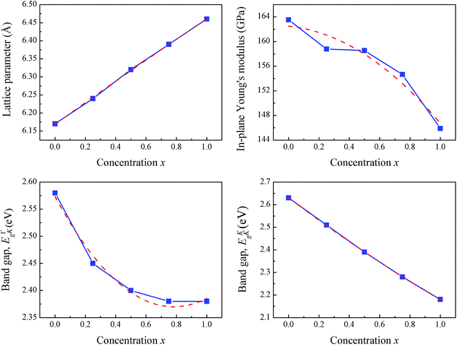 |
| | Fig. 2 The evolution of lattice parameter, Young's modulus and band gap with the concentration x and the corresponding fitted polynomial. | |
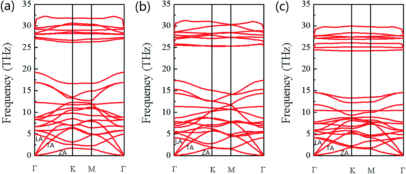
As we explore the applications of Si1−xGexC, it is also necessary to investigate the stability of these ternary alloys. The stability of monolayers SiC and GeC has been reported.14 Herein, only the phonon dispersion curves of Si0.75Ge0.25C, Si0.5Ge0.5C, and Si0.25Ge0.75C are calculated using linear response theory, which are presented in Fig. 3. The configurations of the phonon dispersions of Si1−xGexC are consistent with the results for SiC and GeC in ref. 14. The positive phonon frequencies of all phonon branches indicate that Si0.75Ge0.25C, Si0.5Ge0.5C, and Si0.25Ge0.75C, as described in this work, are dynamically stable. Moreover, the vibrational frequency decreases (phonon softening) with an increase in the Ge concentration. This is consistent with the increase in the lattice constant. As the lattice constant increases with Ge concentration, the vibrational frequency decreases. As we know, the band gap decreases with increasing bond length; thus, the band gap is decreased along with the vibrational frequency as the Ge concentration increases. The details of the band structures of Si1−xGexC will be discussed in the following section. The phonon branches are named according to their eigenvectors at the Γ point. As we can see, the acoustic and optical curves are clearly separated, except that the ZO branches of all the structures fall into the frequency range of the acoustic branches. For our 8-atom cells, there are a total 3 acoustic and 21 optical branches. The three acoustic phonon branches are labeled in Fig. 3; while the in-plane LA and TA modes are linear around the Γ point, the out-of-plane ZA mode displays a quadratic dispersion near the Γ point. This is because the forces relevant to the transverse motion decay rapidly.49 In addition, it is reported that LA and TA branches play a primary role in thermal conductivity compared to the ZA branch.50 These characteristics are consistent with the previous study of monolayers SiC and GeC.14
 |
| | Fig. 3 Phonon dispersions of (a) Si0.75Ge0.25C, (b) Si0.5Ge0.5C, and (c) Si0.25Ge0.75C. | |
The electronic structures
As demonstrated in numerous previous studies, monolayers SiC and GeC have indirect and direct band gaps of ∼2.5 eV and ∼2.1 eV, respectively.14 Herein, the band structures of a 2 × 2 × 1 SiC and GeC supercell are displayed in Fig. 4, along with that of Si1−xGexC (x = 0.25, 0.5, and 0.75). The results show that the incorporation of Ge in SiC does affect the electronic properties of the host material. As shown in Table 1, the band structure of the SiC supercell features an indirect band gap (ΔK–Γ) of 2.58 eV, whereas the band structure of the GeC supercell shows a direct band gap (ΔK–K) of 2.18 eV. The band structures of Si1−xGexC (x = 0.25, 0.5 and 0.75) transform from indirect (ΔK–Γ) to direct (ΔK–K) as x increases. Monolayer Si0.75Ge0.25C has an indirect band gap (ΔK–Γ) of 2.45 eV, whereas monolayer Si0.25Ge0.75C clearly shows a direct band gap (ΔK–K) of 2.28 eV. For Si0.5Ge0.5C, the curve between the K and M points of the conduction band edge are almost flat (indirect 2.40 eV at ΔK–Γ and direct 2.39 eV at ΔK–K); therefore, this is the point of transition from indirect to direct band gap. Moreover, the band gap is found to decrease with increasing Ge concentration. This decrease of the band gap after the incorporation of Ge may be caused by the strain induced. Ge has a larger radius than those of C and Si, resulting in increased lattice parameters and distortion of the structure when Si is substituted by Ge. As demonstrated above, the bond lengths of Si–C and Ge–C fall into two different categories: Ge–C bonds are under compressive strain, as are Si–C bonds close to the Ge atom, whereas Si–C bonds far from the Ge atom are under tensile strain. Since band gaps increase with decreasing bond length, the band gaps of our structures are mainly dependant on extended Si–C bonds in the case of Si0.75Ge0.25C and on compressed Ge–C bonds in cases of Si0.25Ge0.75C and Si0.5Ge0.5C. This conclusion is supported by the density of states analysis detailed below.
 |
| | Fig. 4 Band structures of monolayer SiC, Si0.75Ge0.25C, Si0.5Ge0.5C, Si0.25Ge0.75C, and GeC. | |
In order to clarify the formation of the energy gap, partial densities of states (PDOS) of monolayers SiC, GeC, and Si1−xGexC (x = 0.25, 0.5, and 0.75) are shown in Fig. 5. For all five cases, the valence band edges (VBEs) are mainly composed of C-2p states. For monolayers SiC and GeC, the conduction band edges (CBEs) are dominated by the Si-3p and Ge-4p states, respectively. For ternary Si1−xGexC, the band gaps transform from indirect (ΔK–Γ) to direct (ΔK–K) with an increase of x from 0.25 to 0.75; the main composition of the CBE changes from Si-3p states to Ge-4p states. The band states between −15 and −10 eV in the valence band are mainly derived from C-2s orbitals with small contributions from Si-3s and -3p, and Ge-4s and -4p orbitals. The band states between −8 and 0 eV are mainly derived from C-2p orbitals with small contributions from Si-3s and -3p, and Ge-4s and -4p orbitals. The contributions from the Si-3s and -3p orbitals decrease with increasing Ge concentration, while that of the Ge-4s and -4p orbitals increase. The conduction band states mainly originate from Si-3p and Ge-4p orbitals; the contributions from these orbitals follow a similar trend of decreasing and increasing, respectively, with increases in Ge concentration. Furthermore, the CBE for Si0.75Ge0.25C is mainly derived from the Si-3p states, and moves to a lower energy level compared to the CBE of SiC. This is consistent with the increase in Si–C bond length and shrinking of the band gap compared to that of SiC. For Si0.5Ge0.5C, the contributions from Si-3p and Ge-4p are almost the same, and the CBE continues to move to lower energy level. In contrast, the CBE of Si0.25Ge0.75C is mainly derived from the Ge-4p states and is in a higher level compared to the CBE of GeC. This is consistent with the decrease in Ge–C bond length and increase in band gap compared to GeC.
 |
| | Fig. 5 The partial density of states (PDOS) of monolayer (a) SiC, (b) Si0.75Ge0.25C, (c) Si0.5Ge0.5C, (d) Si0.25Ge0.75C, and (e) GeC. | |
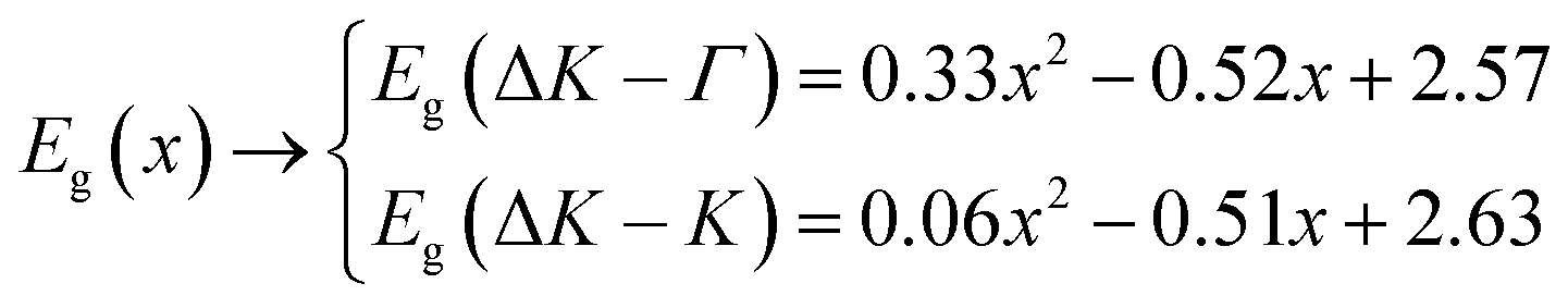
The same method that was used in calculating the bowing parameter of lattice parameter and Young's modulus was also used to obtain the band gap bowing coefficient θ. Small deviation in band gaps of the relaxed structures from the theoretical ones obtained from Vegard's law can be seen from the data in Table 1. The calculated band gap along the ΔK–Γ and ΔK–K direction versus concentration x is fitted by polynomials equations as follows:
| |
 | (8) |
The calculated band gap bowing parameter exhibits a weak composition dependence for both conditions: 0.33 for Eg(ΔK–Γ) and 0.06 for Eg(ΔK–K).
To better comprehend the physical origins of the composition-dependent bowing in monolayer Si1−xGexC sheet, the procedure reported by Bernard and Zunger,51 to decompose the total bowing parameter θ into physically distinct contributions, is used herein. First, the overall bowing parameter coefficient of monolayer Si1−xGexC at concentration x, which amounts to the change in band gap, is expressed in the following format:
| | |
xGeC(aGeC) + (1 − x)SiC(aSiC) → Si1−xGexC(aeq)
| (9) |
where
aSiC and
aGeC are the lattice parameters of the relaxed monolayers SiC and GeC. A general representation of the composition-dependent band gap of monolayer Si
1−xGe
xC in terms of the band gaps of monolayers SiC and GeC, as well as the total bowing parameter
θ, is as follows:
| | |
ESiGeC(x) = (1 − x)ESiC(aSiC) + xEGeC(aGeC) − bx(1 − x)
| (10) |
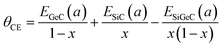
The calculated gap bowing for monolayer Si1−xGexC ranges from −0.423 eV (x = 0.25) to −0.165 eV (x = 0.75). Then, following the procedure of Bernard and Zunger, the total bowing parameter θ can be decomposed into: (1) volume deformation term, θVD; (2) charge exchange term, θCE and (3) structure relaxation term, θSR, using the following equations:
where,
θVD,
θCE, and
θSR are calculated as follows:
| |
 | (12) |
| |
 | (13) |
| |
 | (14) |
These equations quantify the volume deformation (VD), charge exchange (CE), and structure relaxation (SR) effects on the band gap bowing. The θVD part measures the relative response of the band structure of monolayers SiC and GeC to hydrostatic pressures that are induced from the change of their individual lattice parameters to the ternary alloy value a = a(x). The θCE part reflects a charge transfer effect, which in this case means the rearrangement of the energy bands due to the different bonding behavior of Si–C and Ge–C bonds at the lattice parameter a. The θSR measures changes in passing from the unrelaxed structure to the relaxed structure.
The bowing coefficient θ and its three components, θVD, θCE, and θSR, have been calculated at different concentrations (x = 0.25, 0.5 and 0.75), and the results are listed in Table 2. The following facts are discovered:
Table 2 Calculated bowing parameter θ for monolayer Si1−xGexC, and the contributions due to volume deformation (θVD), electronegativity (θCE), and structural relaxation (θSR)
| Composition x |
0.25 |
0.5 |
0.75 |
| θSR |
−1.080 |
−1.046 |
−1.021 |
| θCE |
0.045 |
0.048 |
−0.113 |
| θVD |
0.612 |
0.819 |
0.969 |
| θ |
−0.423 |
−0.179 |
−0.165 |
(i) The volume-deformation term θVD is relatively small, an observation that can be attributed to the small lattice mismatch between monolayers SiC and GeC (≈4.5%). Thus, the disorder in the bond lengths of Si–C and Ge–C induced by relaxation of Si1−xGexC has little influence on the total gap bowing.
(ii) The charge exchange term θCE is even smaller than θVD. The θCE depends on the electronegativity mismatch between Si and Ge atoms. It has been reported that the θCE values for SiSn, GeSn, and SiGe are 1.52,52 0.54,53 and 0.1 eV,54,55 respectively. Si and Ge have a very small electronegativity mismatch, and hence the small values of θCE for Si1−xGexC make sense.
(iii) The structural relaxation term θSR is relatively larger than the other two terms, which means structure relaxation dominates the bowing parameter. This primary role of structure relaxation in the overall bowing parameter implies that atom displacement during structure relaxation plays an important role in the changes of the band structures.
Thermodynamic properties
In order to get some insight into the thermal stability of monolayer Si1−xGexC towards decay into random alloys or elemental constituents, we analyze the thermodynamics of the monolayer Si1−xGexC. Stability can be evaluated by calculating the enthalpy of formation (ΔH)56 according to the following equation:| | |
ΔH(Si1−xGexC) = E(Si1−xGexC) − (1 − x)E(SiC) − xE(GeC)
| (15) |
where E(SiC), E(GeC), and E(Si1−xGexC) are the free energies of monolayers SiC, GeC, and Si1−xGexC, respectively. The calculated ΔH values of monolayers Si0.75Ge0.25C, Si0.5Ge0.5C, and Si0.25Ge0.75C are 10.1 meV per atom, 5.6 meV per atom, and 3.9 meV per atom, respectively. Notice that the positive values of ΔH for monolayers Si0.75Ge0.25C, Si0.5Ge0.5C, and Si0.25Ge0.75C indicate the tendency of these ternary alloys to decompose into their constituent elements, and that the small values of ΔH suggest low critical temperatures. The T–x phase diagrams are calculated based on the methods described in ref. 57–59, along with the critical temperature for miscibility. First, the Gibbs free energy of mixing ΔGm is determined by the following equation:where| |
ΔSm = −R[x![[thin space (1/6-em)]](https://www.rsc.org/images/entities/char_2009.gif) lnx + (1 − x)ln(1 − x)] lnx + (1 − x)ln(1 − x)]
| (18) |
where ΔHm and ΔSm are the enthalpy and entropy of mixing, and Ω, R, and T are the interaction parameter, gas constant, and absolute temperature, respectively. Second, we calculate Ω as a function of concentration x from ΔH (eqn (15)): Ω (meV per atom) = 65.43 − 66.14x is obtained from a linear fit. An average value of 32.36 meV per atom for Ω in the range 0 ≤ x ≤ 1 is then calculated. By calculating ΔGm as a function of concentration x, we determine the T–x phase diagram, which could identify the stable, metastable, and unstable mixing areas of Si1−xGexC for a given temperature. The T–x phase diagram is composed of two curves, i.e., the binodal curve and the spinodal curve. The binodal curve indicates coexistence of two distinct phases, and occurs right below Tc. Beneath the binodal curve is the spinodal curve, which marks the limit of local stability with respect to small fluctuations. The binodal and spinodal curves connect at the critical temperature Tc. In this study, the two binodal points are determined as the points where the common tangent line touches the ΔGm curves. The two spinodal points are considered as the points at which the second derivative of ΔGm is zero, or ∂2(ΔGm)/∂x2 = 0. Because of the use of average values for x-dependent Ω, our phase diagram shows symmetric behavior. Fig. 6 shows the calculated T–x phase diagram. A critical temperature Tc of 187.45 K is observed. The area between the binodal and spinodal curves is where the alloy may exist as a metastable phase. The low critical temperature of monolayer Si1−xGexC indicates that this alloys is stable only at low temperatures.
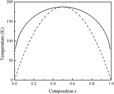 |
| | Fig. 6 T–x phase diagram of monolayer Si1−xGexC. The solid line is binodal curve and the dashed line is spinodal curve. | |
Conclusion
In summary, we studied the structural parameters, electronics, and thermodynamic properties of relaxed monolayer Si1−xGexC (x = 0.25, 0.5, and 0.75) by performing first-principles pseudopotential plane-wave calculations. Bowing parameters of 0.364 and −1.23 are found for the lattice parameters and in-plane Young's modulus, whereas bowing parameter of 0.33 and 0.06 are found for Eg(ΔK–Γ) and Eg(ΔK–K). The band gap decreases from 2.58 eV to 2.18 eV as the Ge concentration increases from 0 to 1 equivalents. An indirect to direct band gap transition is observed at about x = 0.5. Our results suggest that the structure relaxation has a dominant effect on the bowing parameter. The phonon dispersion curves also indicate that our structures are dynamically stable. The calculated phase diagram shows a critical temperature of 187.45 K and illustrates the stable, metastable, and unstable mixing regions of the alloy. These characteristics provide a new method to modify the electronic properties of 2D-SiC, which carries great importance for applications in optoelectronic devices.
Acknowledgements
This study is supported by the Aviation Science Fund (Grant no. 2015ZF53073), the Open Research Fund of State Key Laboratory of Transient Optics and Photonics (Chinese Academy of Sciences) (Grant no. SKLST201503), the Fund of the State Key Laboratory of Solidification Processing (NWPU, China) (Grant no. 110-QP-2014).
References
- G. L. Harris, Properties of Silicon Carbide, INSPEC Institution of Electrical Engineers, London, 1995 Search PubMed.
- P. A. Ivanov and V. E. Chelnokov, Semicond. Sci. Technol., 1992, 7, 863 CrossRef CAS.
- W. J. Choyke, H. Matsunami and G. Pensl, Silicon Carbide: Recent Major Advances, Springer-Verlag Berlin, 2004 Search PubMed.
- K. S. Novoselov, A. K. Geim, S. V. Morozov, D. Jiang, Y. Zhang, S. V. Dubonos, I. V. Grigorieva and A. A. Firsov, Science, 2004, 306, 666 CrossRef CAS PubMed.
- M. I. Katsnelson, K. S. Novoselov and A. K. Geim, Nat. Phys., 2006, 2, 620 CrossRef CAS.
- K. S. Novoselov, A. K. Geim, S. V. Morozov, D. Jiang, M. I. Katsnelson, I. V. Grigorieva, S. V. Dubonos and A. A. Firsov, Nature, 2005, 438, 197 CrossRef CAS PubMed.
- C. Itzykson and J. B. Zuber, Quantum Field Theory, Dover, New York, 2006 Search PubMed.
- Y. B. Zhang, Y. W. Tan, H. L. Stormer and P. Kim, Nature, 2005, 438, 201 CrossRef CAS PubMed.
- C. Berger, Z. Song, T. Li, X. Li, A. Y. Ogbazghi, R. Feng, Z. Dai, A. N. Marchenkov, E. H. Conrad, P. N. First and W. A. De Heer, Science, 2006, 312, 1191 CrossRef CAS PubMed.
- X. Du, I. Skachko, A. Barker and E. Y. Andrei, Nat. Nanotechnol., 2008, 3, 491 CrossRef CAS PubMed.
- M. S. Fuhrer, C. N. Lau and A. H. MacDonald, MRS Bull., 2010, 35, 289 CrossRef CAS.
- C. Xia, L. I. Johansson, Y. Niu, A. A. Zakharov, E. Janzén and C. Virojanadara, Carbon, 2014, 79, 631 CrossRef CAS.
- H. Li, Q. Zhang, C. Liu, S. H. Xu and P. Q. Gao, ACS Nano, 2011, 5(4), 3198 CrossRef CAS PubMed.
- H. Sahin, S. Cahangirov, M. Topsakal, E. Bekaroglu, E. Akturk, R. T. Senge and S. Ciraci, Phys. Rev. B: Condens. Matter Mater. Phys., 2009, 80, 155453 CrossRef.
- H. C. Hsueh, G. Y. Guo and S. G. Louie, Phys. Rev. B: Condens. Matter Mater. Phys., 2011, 84, 085404 CrossRef.
- L. Sun, Y. F. Li, Z. Y. Li, Q. X. Li, Z. Zhen, Z. F. Chen, J. L. Yang and J. G. Hou, J. Chem. Phys., 2008, 129, 174114 CrossRef PubMed.
- P. Lou and J. Y. Lee, J. Phys. Chem. C, 2009, 113, 12637 CAS.
- S. S. Lin, J. Phys. Chem. C, 2012, 116, 3951 CAS.
- E. Bekaroglu, M. Topsakal, S. Cahangirov and S. Ciraci, Phys. Rev. B: Condens. Matter Mater. Phys., 2010, 81, 075433 CrossRef.
- M. B. Javan, J. Magn. Magn. Mater., 2016, 401, 656 CrossRef.
- C. D. Costa and J. M. Morbec, J. Phys.: Condens. Matter, 2011, 23, 205504 CrossRef CAS PubMed.
- B. Xu, J. Yin, Y. D. Xia, X. G. Wan and Z. G. Liu, Appl. Phys. Lett., 2010, 96, 143111 CrossRef.
- Y. D. Ma, Y. Dai, M. Guo, C. W. Niu, L. Yu and B. B. Huang, Appl. Surf. Sci., 2011, 257, 7845 CrossRef CAS.
- L. Yuan, Z. Y. Li and J. L. Yang, Phys. Chem. Chem. Phys., 2013, 15, 497 RSC.
- B. L. Gao, Q. Q. Xu, S. H. Ke, N. Xu, G. Hu, Y. Z. Wang, F. Liang, Y. L. Tang and S. J. Xiong, Phys. Lett. A, 2014, 378, 565 CrossRef CAS.
- X. Lin, S. S. Lin, Y. Xu, A. A. Hakro, T. Hasan, B. L. Zhang, B. Yu, J. K. Yu, E. P. Li and H. S. Chen, J. Mater. Chem. C, 2013, 1, 2131 RSC.
- T. Y. Lü, X. X. Liao, H. Q. Wang and J. C. Zheng, J. Mater. Chem., 2012, 22, 10062 RSC.
- Z. Xu, Y. P. Li, Z. T. Liu and C. X. Li, Physica E: Low-Dimensional Systems & Nanostructures, 2016, 79, 198 CAS.
- M. H. Wu, Y. Pei and X. C. Zeng, Chem. Phys. Lett., 2013, 580, 78 CrossRef CAS.
- P. Lou, J. Mater. Chem. C, 2013, 1, 2996 RSC.
- N. Alaal, V. Loganathan, N. Medhekar and A. Shukla, J. Phys. D: Appl. Phys., 2016, 49, 105306 CrossRef.
- L. Pan, H. J. Liu, Y. W. Wen, X. J. Tan, H. Y. Lv, J. Shi and X. F. Tang, Phys. Lett. A, 2011, 375, 614–619 CrossRef CAS.
- Z. Xu, Y. P. Li, C. X. Li and Z. T. Liu, Appl. Surf. Sci., 2016, 367, 19–25 CrossRef CAS.
- L. B. Drissi and F. Z. Ramadan, Physica E: Low-Dimensional Systems & Nanostructures, 2015, 74, 377–381 CAS.
- Q. Peng, C. Liang, W. Ji and S. De, Mech. Mater., 2013, 64, 135–141 CrossRef.
- I. Guilhon, L. K. Teles and M. Marques, Phys. Rev. B: Condens. Matter Mater. Phys., 2015, 92, 075435 CrossRef.
- A. G. Gökce and E. Aktürk, Appl. Surf. Sci., 2015, 332, 147–151 CrossRef.
- Z. W. Chen, M. Y. Lv and R. P. Liu, J. Appl. Phys., 2005, 98, 096105 CrossRef.
- K. J. Roe, G. Katulka, J. Kolodzey, S. E. Saddow and D. Jacobson, Appl. Phys. Lett., 2001, 78, 2073 CrossRef CAS.
- C. Guedj and J. Kolodzey, Appl. Phys. Lett., 1999, 74, 691 CrossRef CAS.
- G. Katulka, K. J. Roe, J. Kolodzey, C. P. Swann, G. Desalvo, R. C. Clarke, G. Eldridge and R. Messham, J. Electron. Mater., 2002, 31, 346 CrossRef CAS.
- M. D. Segall, P. L. D. Lindan, M. J. Probert, C. J. Pickard, P. J. Hasnip, S. J. Clark and M. C. Payne, J. Phys.: Condens. Matter, 2002, 14, 2717 CrossRef CAS.
- P. Zhang, V. H. Crespi, E. Chang, S. G. Louie and M. L. Cohen, Nature, 2001, 409, 69 CrossRef CAS PubMed.
- C. Raffy, J. Furthmüller and F. Bechstedt, Phys. Rev. B: Condens. Matter Mater. Phys., 2002, 66, 075201 CrossRef.
- D. Vanderbilt, Phys. Rev. B: Condens. Matter Mater. Phys., 1990, 41, 7892 CrossRef.
- J. P. Perdew, K. Burke and M. Ernzerhof, Phys. Rev. Lett., 1996, 77, 3865 CrossRef CAS PubMed.
- L. Vegard, Z. Phys., 1921, 5, 17 CrossRef CAS.
- M. Ameri, N. Bouzouira, R. Khenata, Y. Al-Douri, B. Bouhafs and S. Bin-Omran, Mol. Phys., 2013, 111(21), 3208–3217 CrossRef CAS.
- F. Liu, P. Ming and J. Li, Phys. Rev. B: Condens. Matter Mater. Phys., 2007, 76, 064120 CrossRef.
- P. G. Klemens, Int. J. Thermophys., 2001, 22, 265 CrossRef CAS.
- J. E. Bernard and A. Zunger, Phys. Rev. B: Condens. Matter Mater. Phys., 1987, 36, 3199 CrossRef CAS.
- M. Ferhat and A. Zaoui, Infrared Phys., 2001, 42, 81 CAS.
- Y. Chibane, B. Bouhafs and M. Ferhat, Phys. Status Solidi B, 2003, 240, 116 CrossRef CAS.
- F. Tekia, M. Ferhat and A. Zaoui, Phys. B, 2000, 293, 183 CrossRef CAS.
- H. C. Zhou, M. W. Zhao, X. M. Zhang, W. Z. Dong, X. P. Wang, H. X. Bu and A. Z. Wang, J. Phys.: Condens. Matter, 2013, 25, 395501 CrossRef PubMed.
- J. L. Martins and A. Zunger, Phys. Rev. Lett., 1986, 56, 1400 CrossRef CAS PubMed.
- R. A. Swalin, Thermodynamics of Solids, Wiley, New York, 1961 Search PubMed.
- L. G. Ferreira, S. H. Wei, J. E. Bernard and A. Zunger, Phys. Rev. B: Condens. Matter Mater. Phys., 1999, 40, 3197 CrossRef.
- L. K. Teles, J. Furthmüller, L. M. R. Scolfaro, J. R. Leite and F. Bechstedt, Phys. Rev. B: Condens. Matter Mater. Phys., 2000, 62, 2475 CrossRef CAS.
|
| This journal is © The Royal Society of Chemistry 2016 |
Click here to see how this site uses Cookies. View our privacy policy here.