DOI:
10.1039/C6RA09109A
(Paper)
RSC Adv., 2016,
6, 82581-82590
Physical vapor deposited highly oriented V2O5 thin films for electrocatalytic oxidation of hydrazine†
Received
8th April 2016
, Accepted 16th August 2016
First published on 24th August 2016
Abstract
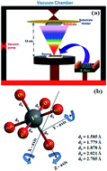
The proposed work is focused on the effect of substrates on the electrocatalytic performance of physical vapor deposited vanadium pentoxide (V2O5) films. V2O5 thin films were prepared onto various substrates such as glass, indium doped tin oxide (ITO), fluorine doped tin oxide (FTO), aluminum (Al) and copper (Cu). XRD patterns revealed that the evaporated V2O5 films were a single crystalline orthorhombic structure with the predominant orientation along the (001) lattice plane. In order to understand the influence of substrates' effect on the structural properties, various microstructural parameters such as crystallite size (D), dislocation density (δ), microstrain (ε) texture coefficient and stacking fault probability (α) for preferential orientation were evaluated and discussed in detail. Tauc's plot was used to determine the band gap of V2O5 thin films and found to be 2.1 eV for the film deposited on the ITO substrate. SEM and AFM analyses revealed that physical vapored V2O5 thin films are densely packed with uniform morphological and topographical features. Significantly, to the best of our knowledge; the feasibility of V2O5 thin films for the electrochemical performance towards the detection of hydrazine oxidation was demonstrated for the first time using cyclic voltammetric studies. V2O5 thin films coated on ITO substrates exhibited better catalytic activity with a mass catalytic activity of 3320 mA g−1. These findings will provide a new avenue for electrocatalytic activity of hydrazine oxidation based on V2O5 thin films and will be extremely important for the selection of a suitable substrate in the field of sensor and actuator technology.
Introduction
Transition-metal oxides are renowned for their structural versatility combined with chemical and physical properties.1–3 Particularly, vanadium oxides represent an important class of systems in view of their novel material characteristics that are widely studied and used in many scientific and technological applications.4,5 Amidst all vanadium oxides, V2O5 is the most saturated (highest oxidation state) oxide in the V–O system, consequently the most stable one and crystallizing with an orthorhombic structure.6 Additionally, V2O5 having a relatively narrow bandgap of 2.2 eV in comparison with the widely used metal oxides such as ZnO (3.4 eV) or SnO2 (3.7 eV), which makes as a promising worthwhile material for the researcher community.7,8 Vanadium oxide in the form of thin film have attracted significant attention in the recent years owing to their fascinating properties such as multivalancy ranging from V2+ to V5+, wide optical band gap, good chemical and thermal stability.9,10 These properties make V2O5 thin films are suitable candidate for scientific, industrial and technological applications, including catalytic material in gas sensors,11,12 as a dielectric constituent material in super capacitors,13 as a high capacity storage medium in Li-ion batteries, as a cathode in these batteries,14 or as a thermo-resistive material in thermal infrared detectors.15
In addition, V2O5 is an excellent catalyst for a number of reactions like selective oxidation, selective reduction, and dehydrogenation of hydrocarbons and other organic compounds.16,17 V2O5 has interesting physical properties and characterized by a rich chemistry, which somehow mirrors the diversity of possible vanadium formal oxidation states and the variability of oxygen coordination geometries.18 The catalytic oxidation reactions in V2O5 have been discussed based on the reduction–oxidation mechanism proposed by Mars–van Krevelen, where lattice oxygen is transferred to the reacting gas molecules. This implies that reduced sites will invariably form at the surface of oxide during the catalytic reactions, even though they might be transient states.19 It is actually often claimed that depending on the respective reaction and the reaction conditions, lower oxidation states of vanadium play a vital role in the catalytic process on the V2O5 based catalysts.4,20–22 For instance, the interaction of gas phase O2 with the reduced sites may lead to activated oxygen species that can participate in the reactions.23
Fuel cells based on carbon free hydrazine liquid fuel have own many advantages such as high theoretical cell voltage of 1.61 V, high power density, high hydrogen content, easy to transportation and storage, and no greenhouse gas emission.24 Hydrazine is an ideal candidate fuel for direct liquid fuel cell system from the viewpoint that the fuel electro-oxidation process does not suffer from any poisoning effects and no CO-like intermediate poisoning species.25,26 Moreover, a catalyst is requisite to improve the oxidation efficiency in the hydrazine oxidation process. Therefore, lot of electrocatalysts have been explored by the electrochemists and investigated extensively including silver,27 gold,28 nickel,29,30 palladium and palladium-based compounds,31,32 platinum,33 cobalt34–36 and carbon materials.37–39 However, the high cost and scarcity limits the utilization of noble metals as electrode materials in fuel cell at a large scale commercial applications even though they exhibit high electrocatalytic activities. Therefore, considerable interests have been turned out towards the developing cheap and sustainable noble metal-free electrocatalysts for the hydrazine oxidation. Transition metal oxides are extremely attractive as catalysts owing to their extraordinarily catalytic activities for oxidation reactions. Despite the enormous importance, V2O5 is still not used as an electrocatalysts for hydrazine oxidation, which inspired us to explore V2O5 in the aforementioned area.
However, the electrocatalytic activity depend on the deposition process and parameters of the films, while catalytic performance are closely related with the catalyst morphology, grain size, surface texture, crystalline structure. Several methods were used for the preparation of V2O5 thin films such as spray pyrolysis,40 RF sputtering,41 electrodeposition,42 pulsed laser deposition,43 chemical methods,44 thermal evaporation45 etc. Among them, electron beam – physical vapor deposition (EB-PVD) yields high quality, uniform and large scale deposition suitable for various applications in research and industries.46 In this communication, highly oriented V2O5 thin films were deposited on the various conducting substrates by electron beam physical vapor evaporation method and study their electro-catalysis of hydrazine oxidation for the first time to the best of our knowledge.
Experimental
V2O5 thin films were deposited by an electron beam evaporation technique using an electron beam gun evaporator (HINDHIVAC vacuum coating unit model 12A4D with electron beam power supply model EBG-PS-3K) under a chamber pressure of 10−5 mbar. The pelletized V2O5 (purity ∼ 99.99%) was taken in graphite crucibles, kept on water-cooled copper hearth of the electron gun, inside the vacuum chamber. The surface of V2O5 pellets was scanned by the resultant and deflected electron beam with an accelerating voltage of 5 kV. The vapor phase of the evaporated material was condensed and deposited as a thin film layer on the surface of the substrates. The distance between source and substrate was maintained at 12 cm. Substrate temperature (TS) was maintained at 473 K throughout all experiments. Various substrates such as indium doped tin oxide (ITO), fluorine doped tin oxide (FTO), copper (Cu), aluminium (Al) and glass were used to deposit V2O5 thin films. The substrates were ultrasonically cleaned using isopropyl alcohol and acetone for 30 minutes and then rinsed in deionized water. The detailed experimental set up and crystal structure of V2O5 are provided in the schematic diagram of Fig. 1.
![image file: c6ra09109a-f1.tif](/image/article/2016/RA/c6ra09109a/c6ra09109a-f1.gif) |
| Fig. 1 (a) Schematic diagram of V2O5 thin film deposition by EB-PVD. (b) Structure of V2O5 unit cell. | |
V2O5 thin films thickness was measured using a stylus profilometer (Mitutoyo SJ-301) equipped with a diamond needle. X-ray diffractograms were recorded using an X'PERT PRO Panalytical diffractometer using Cu-Kα (λ = 0.154 nm) as the source radiation over the range 10–80°. Micro-Raman analyses were carried out using Princeton Acton SP 2500 instrument monochromator with 0.5 focal length grating. Raman scattering measurements were performed using 514.5 nm excitation line from an Ar+ laser. Morphological analyses were done using a FEI QUANTA scanning electron microscope (SEM). Atomic force microscopy (AFM) analysis was used for topographical studies. The optical properties were studied using a UV-Vis spectrophotometer (Perkin Elmer Lamda 9). Luminescence properties were obtained using a Cary Eclipse fluorescence spectrophotometer using a 330 nm Xe laser as the excitation source at room temperature. The electrocatalytic activity for the hydrazine oxidation of V2O5 thin films were systematically investigated through cyclic voltammetry in 50 mM NaOH with 0.1 M hydrazine hydrate using a three-electrode setup consisting of saturated Ag/AgCl as a reference electrode, platinum wire as a counter electrode and V2O5 as a working electrode.
Results and discussion
Structural and microstructural studies
V2O5 thin films were deposited onto different substrates such as ITO, FTO, Cu, Al and glass, using electron beam evaporation method. The prepared films were systematically investigated using various characterization techniques to elucidate the physical properties of deposited films and electrocatalytic properties. Fig. 2(a) shows XRD patterns of V2O5 thin films deposited on different substrates. The observed diffraction lines are indexed with standard diffraction data [JCPDS card no. #41-1426]. The predominant orientation of V2O5 thin film is exhibited at an angle 20.26° corresponding to the lattice orientation of (001) which is in good agreement with the standard value. It revealed the orthorhombic structure with Pmmn space group symmetry and D2h point group with the lattice constants a = 11.51 Å, b = 3.56 Å and c = 4.37 Å. The crystalline structure of V2O5 projected along (001) lattice plane is shown in Fig. 1(b).
![image file: c6ra09109a-f2.tif](/image/article/2016/RA/c6ra09109a/c6ra09109a-f2.gif) |
| Fig. 2 (a) XRD patterns of V2O5 thin films deposited on different substrates. (b) Peak broadening along (001) plane. (c) Variation of FWHM and d-spacing values in terms of deposition substrates. | |
The predominant orientation of V2O5 thin film is exhibited at an angle 20.26° corresponding to the lattice orientation of (001) which is in good agreement with the standard value. It revealed the orthorhombic structure with Pmmn space group symmetry and D2h point group with the lattice constants a = 11.51 Å, b = 3.56 Å and c = 4.37 Å. The crystalline structure of V2O5 projected along (001) lattice plane is shown in Fig. 1(b).
V2O5 thin films coated on Cu, Al and FTO substrates exhibited orientation along (001) plane with orthorhombic structure.47–49 From Fig. 2(a), XRD pattern for V2O5 thin film prepared on ITO substrate revealed the peak position 2θ at 20.26° and 41.26° corresponding to (001) and (002) lattice planes, respectively. Moreover, V2O5 thin films prepared on glass substrates exhibited diffraction pattern with (001) and (002) lattice planes. This observation reveals that the crystalline nature of evaporated films is influenced by the nature of the employed substrate. Also, the intensity of metallic peaks of Cu and Al is higher than the (001) peak of V2O5 thin films grown on it due to the inherent crystalline nature of these metallic substrates. Hence the (001) peak intensity of V2O5 thin films are low compared with the other substrates (glass, ITO and FTO). The crystallinity is quite low for V2O5 thin films prepared on Cu and Al substrates compared with films prepared on other substrates. Also, no other impurities or other secondary phases of vanadium and oxygen are evident from the diffraction lines in the XRD pattern. This result indicates that our deposited films belong to pure V2O5 with single phase.
The estimation of film thickness is carried out using a stylus surface profilometer. Lower film thickness is observed for V2O5 thin films prepared on Cu substrate and the estimated value is ∼1160 nm. The films thicknesses prepared on Al, FTO, ITO and glass substrates are 1174, 1185, 1190 and 1200 nm, respectively. The maximum value of film thickness is observed for V2O5 thin films prepared on glass substrate which may be due to intrinsic adherence properties of the substrate. The substrate surface and nature of the adherence properties are much important to enhance the film quality and thickness of the deposited film.
The broadening of the peak is obviously found to vary by the type of substrate as shown in Fig. 2(b). The peak shift towards lower diffraction angle may be noted for FTO, Cu and Al substrates. This may be attributed to the higher degree of lattice mismatch and uneven thermal expansion coefficients. The predominant peak orientation of V2O5 thin films prepared on glass and ITO substrates is highly dependent with standard values as shown in Fig. 2(b). The variations of full-width at half maximum (FWHM) and d-spacing values for V2O5 thin films prepared on different substrates are presented in Fig. 2(c). The maximum value of FWHM is observed for films prepared on ITO substrate and lower value is exhibited for films prepared on Cu substrate. Such behavior reflects the decreased contribution of lattice imperfections. FWHM plays a prominent role to evaluate microstructural properties of prepared V2O5 thin films. The d-spacing values are estimated for films prepared on various substrates and it has slightly varied by the type of substrate as shown in Fig. 2(c). This difference is higher for films coated on Cu, Al and FTO substrates compared with those coated on glass and ITO substrates.
The crystallite size, microstrain, dislocation density and stacking fault probability values for V2O5 thin films are given in Table 1. The crystallite size of the films is calculated from the Debye Scherer's46,50 formula using full-width at half-maximum intensity (FWHM) expressed in radians
|
![image file: c6ra09109a-t1.tif](/image/article/2016/RA/c6ra09109a/c6ra09109a-t1.gif) | (1) |
where ‘
D’ is crystallite size and ‘
β’ is full width at half maximum (FWHM). The variation of crystallite size of V
2O
5 thin films prepared on various substrates is shown in
Table 1. The lower crystallite size is observed for the film deposited on ITO coated glass substrate which is consistent with FWHM values. From the above results, we infer that the nature of substrates play a predominant role on the microstructural properties of deposited films. The micro strain ‘
ε’ is calculated using the relation,
|
![image file: c6ra09109a-t2.tif](/image/article/2016/RA/c6ra09109a/c6ra09109a-t2.gif) | (2) |
where
λ is wavelength,
D is crystallite size,
β is FWHM of the predominant orientation and
θ is Bragg's angle. From the
Table 1, microstrain values are found to vary with the type of substrate employed to deposit V
2O
5 thin films. The microstrain values of the films deposited on glass, ITO, FTO, Cu and Al are found to be 0.025, 0.028, 0.014, 0.024 and 0.023, respectively. The lower value of microstrain is obtained for FTO coated glass substrate. The microstrain variation of V
2O
5 thin films is due to the crystallite size alteration on different substrates. The dislocation density ‘
δ’ defined as the length of dislocation lines per unit volume of the crystal, is evaluated from the crystallite size
D and microstrain (
ε) by the relation,
|
![image file: c6ra09109a-t3.tif](/image/article/2016/RA/c6ra09109a/c6ra09109a-t3.gif) | (3) |
where ‘
a’ is lattice constant. The estimated dislocation density values are presented in
Table 1 and lower value (0.37 × 10
15 lines per m
2) is observed for V
2O
5 thin films coated on FTO substrates. The dislocation density increases with decrease in crystallite size. The decrease of crystallite size is attributed to the increase of the grain boundaries and the amount of defects in the crystalline structure. The relation for stacking fault probability (
α) with peak shift Δ(2
θ) is given by
|
![image file: c6ra09109a-t4.tif](/image/article/2016/RA/c6ra09109a/c6ra09109a-t4.gif) | (4) |
where
D is crystallite size,
β is full width at half maximum,
α is stacking fault probability and
λ is wavelength of the X-ray diffraction, respectively. The stacking fault probability with various substrates is tabulated in
Table 1. The stacking fault probability value is varied for different substrates which are due to the peak position differences between standard and observed values. The lower values are observed at ITO and glass substrate prepared films due to the lower peak difference as shown in XRD pattern (
Fig. 2(a)). XRD analyses showed that substrate plays a significant role in the microstructural and structural properties of the V
2O
5 films, and the ITO substrate exhibits better properties. The value of dislocation density, microstrain and stacking fault probability are found to be 1.01 × 10
15 lines per m
2, 0.025 and 0.0010 m, respectively, for the V
2O
5 film deposited at ITO substrate. The texture coefficient
51 is calculated from the formula,
|
![image file: c6ra09109a-t5.tif](/image/article/2016/RA/c6ra09109a/c6ra09109a-t5.gif) | (5) |
where
I(
hkl) is the measured relative intensity of a plane (
hkl),
Io(
hkl) is the standard relative intensity of the plane (
hkl) taken from the JCPDS card,
N is the number of reflections.
Table 1 represents the texture coefficient value of (200), (001) and (002) lattice orientation of V
2O
5 thin film prepared on different substrates. The texture coefficient value of predominant (001) peak is found to be 1.4, 1.62, 1.76, 1.72, 1.86 for films deposited on glass, ITO, FTO, Cu and Al substrates, respectively. The single diffraction line exhibited in the diffractogram of V
2O
5 film exhibit higher values because all the atoms are highly textured in unique direction. The texture coefficient value is higher than 1 indicates preferential orientation which has abundance of grains in a given (
hkl) direction. These manifests that the thin films formed are highly oriented along (001) preferential orientation.
Table 1 Microstructural properties of V2O5 thin films deposited on different substrates
Type of substrate |
Crystallite size (nm) |
Dislocation density × (1015 lines per m2) |
Microstrain |
Texture coefficient |
Stacking fault probability |
TC(001) |
TC(002) |
Glass |
31 |
1.01 |
0.025 |
1.40 |
0.63 |
0.0025 |
ITO/glass |
25 |
1.57 |
0.028 |
1.62 |
0.32 |
0.0029 |
FTO/glass |
52 |
0.37 |
0.014 |
1.76 |
0 |
0.0117 |
Cu sheet |
30 |
1.12 |
0.024 |
1.72 |
0 |
0.0084 |
Al sheet |
31 |
1.04 |
0.023 |
1.86 |
0 |
0.0099 |
Raman spectroscopy is an important tool to characterize the structural order–disorder angles at short range and crystallinity of oxide materials. Fig. 3 displays the Raman spectra of V2O5 thin films prepared on different substrates. From the Raman spectra, the prepared film can be assigned to the specific signature of α-V2O5 polymorph.52 The peak intensities indicate that the crystallinity increases from films deposited on Al through glass. Peaks located at 285 cm−1 and 305 cm−1 represents the bending vibrations of V
O bonds and triply coordinated V–O bonds respectively. Peaks at 406 cm−1 and 483 cm−1 corresponds to the bending vibrations of V
O bond and V–O–V bridging bonds respectively. The peak at 525 cm−1 is assigned to the stretching vibrations of V–O–V bond aroused from edge-shared oxygen atoms to three VO5 pyramids. Moreover, asymmetric stretching mode of V–O–V bridging bonds resulted from the corner shared oxygen common to the two VO5 pyramids is exhibited at 701 cm−1. The high frequency peak at 996 cm−1 gives the structural quality of the films and can be ascribed to the stretching mode related to symmetry vibrations of the terminal vanadium oxygen V
O. This value also manifests good stoichiometry of the all the deposited thin films. Also, observed Raman shifts and corresponding mode of vibrations are provided in the ESI Table S1,† which are in good agreement with the earlier reports.44,53–55 These results also establish that the V2O5 thin films are grown preferentially with c-axis oriented perpendicular to the substrate plane. No other peaks representing secondary phases of vanadium and oxygen were observed that ascertains single phase formation. Also, the absence of peak at 850 cm−1 indicated that the films are not hydrated (V2O5·H2O) which is normally observed in V2O5 as contaminant.56 The variations of peak intensity and broadening by type of substrate employed which may be due to lattice-phonon confinement effect.57
![image file: c6ra09109a-f3.tif](/image/article/2016/RA/c6ra09109a/c6ra09109a-f3.gif) |
| Fig. 3 Micro-Raman spectra of V2O5 thin films deposited on different. | |
Morphological studies
Scanning electron microscopy (SEM) is a versatile route to analyze morphological properties of V2O5 films and also to determine the grain size. Fig. 4(a)–(e) shows typical SEM micrographs of V2O5 thin films deposited on different substrates such as glass, Cu, Al, FTO and ITO. The role of substrates on the morphology of the thin films is obviously evident from the SEM micrographs. V2O5 thin films coated on glass and ITO substrates exhibit very densely packed particles with smooth surface morphology. V2O5 thin films coated on various metallic substrates exhibit different particle size owing to their rough surface nature of metals as shown in Fig. 4(b) and (c). V2O5 films coated onto FTO substrate shows that spherically shaped grains as shown in Fig. 4(d) and average particle size is about ∼200 nm. Also, these film surfaces are compact and dense. It is observed that the surface is highly homogenous and is free from pin holes, cracks or voids. No agglomerations are observed on films deposited on the surface of glass, ITO and FTO substrates, whereas slight agglomerations are visible on films using metallic substrates like Al and Cu. Such morphology indicates that the films possess good microstructure. This result is more consistent with XRD findings. These surface properties have strong effect on the optical properties such as transmittance, absorbance and reflection.
![image file: c6ra09109a-f4.tif](/image/article/2016/RA/c6ra09109a/c6ra09109a-f4.gif) |
| Fig. 4 SEM micrographs of V2O5 thin films deposited on (a) glass (b) Cu (c) Al (d) FTO and (e) ITO substrates. | |
Furthermore, surface topological properties of V2O5 thin films are examined using an atomic force microscope (AFM). Fig. 5(a)–(c) shows that two-dimensional (2D) and three-dimensional (3D) topographical images of V2O5 thin films evaporated onto glass, ITO and FTO substrates. The island shaped grains with voids and hillocks are observed in topographical 2D and 3D images of V2O5 thin film deposited on FTO substrate as shown in Fig. 5(a). AFM micrograph demonstrated larger size of grains for V2O5 thin film coated onto FTO substrate compared with films on glass and ITO substrates. Also, in some places coalescence of grains is exhibited due to the agglomeration process. The tightly bounded grains with inhomogeneous size are observed on the surface of V2O5 thin film on ITO substrate as shown in Fig. 5(b). The needle shaped uniform topology of the film is enlightened by AFM 2D and 3D image of V2O5 thin film deposited on glass substrate. 3D images confirmed the grain growth with uniform heights and are highly oriented in particular direction, which is consistent with the XRD and Raman results. AFM 3D microscopic images reveal the granular nature of particles and agglomeration of particles. These images support the SEM data revealing tight packing density. Fig. S2† shows the AFM topography of V2O5 thin films deposited on Cu and Al substrates. V2O5 thin films deposited on Cu substrates exhibits irregularly distributed island of hillocks. Nano grains with voids and pores are observed for V2O5 thin films deposited on Al substrates. The surface interface properties have strongly influenced the morphology of the deposited thin films. These observations are in agreement with observations of SEM. Fig. S1† shows the zoom in image of V2O5 thin films coated on different substrates.
![image file: c6ra09109a-f5.tif](/image/article/2016/RA/c6ra09109a/c6ra09109a-f5.gif) |
| Fig. 5 AFM images of V2O5 thin films deposited on (a) FTO (b) ITO and (c) glass substrates. | |
Optical studies
The transmission spectra are taken at room temperature in air to obtain information about the optical properties of the V2O5 thin films. Fig. 6(a) represents spectral transmittance as a function of wavelength for V2O5 thin films on different substrates measured at normal incidence. It is observed that films prepared on ITO, FTO and glass substrates behave as transparent materials between 450 and 1100 nm wavelength range because of transmittance values are high at these wavelengths. The transmittance values slightly increases in the range 450 to 600 nm and then rapidly increases because of their highly transmitting properties of the films prepared on FTO, glass and ITO, respectively. Besides, as can be seen in Fig. 6(a), the optical transmissions band edge of films deposited on glass, FTO and ITO substrates are approximately equal and these transmission values are changed with respect to the substrate. The transmittance percentage is lying between 55 and 82% in the visible region and it has slightly varied depend on the substrate which may be due to the thickness variation. The interference pattern in transmittance spectra are observed for V2O5 thin films deposited on glass and ITO substrates as shown in Fig. 6(a). This nature can be enabled due to the highly crystalline nature of the film and also it is an obvious evidence for high conductivity nature surface of the film. The absence of interference pattern of V2O5 thin films on FTO substrates may be ascribed to the inhomogeneous surface nature as evident from SEM and AFM micrographs. The band edge is shifted to the higher wavelength region due to the alteration of band gap values. The enhancement of transmittance value might affect optical band edge due to the increment of carrier concentration of the film. This effect of substrate on the transmission of the V2O5 films may be due to the film thickness, structural properties, surface smoothness and defect density.
![image file: c6ra09109a-f6.tif](/image/article/2016/RA/c6ra09109a/c6ra09109a-f6.gif) |
| Fig. 6 (a) Transmittance spectra of V2O5 thin films deposited on different substrates (b) Tauc's plot of V2O5 thin films deposited on different substrates (c) PL spectra of V2O5 thin films deposited on different substrates. | |
Since V2O5 films are n-type materials, their absorption property is a very important optical parameter. The optical parameters such as absorption coefficient and band gap are determined from optical absorption measurements. The value of absorption coefficient for strong absorption region of thin film is calculated using the following eqn (6),
|
![image file: c6ra09109a-t6.tif](/image/article/2016/RA/c6ra09109a/c6ra09109a-t6.gif) | (6) |
where ‘
α’ is the absorption coefficient in cm
−1, ‘
t’ is the thickness of the films, ‘
A’ is absorbance and ‘
T’ is transmittance. The nature of transition is determined using the following
eqn (7),
where ‘
α’ is absorption coefficient in cm
−1, ‘
hν’ is photon energy, ‘
Eg’ is an energy gap, ‘
A’ is energy dependent constant and ‘
n’ is an integer.
The extrapolation of plot to the x-axis gives the band gap energy of V2O5 thin film [Fig. 6(b)]. The energy band gap value of electron beam evaporated V2O5 thin film is found to be 2.1–2.36 eV using Tauc's plot. The indirect band gap energy of V2O5 thin film is found to be 2.36 eV for film synthesized on glass substrates and this value is in good agreement with the earlier report.58 A band gap shift from lower energies to higher energies is also observed due to its thickness alteration by substrate variation.
We have further investigated the experimental data of optical transmittance of thermally evaporated V2O5 thin film to calculate the refractive index and the extinction coefficient. The refractive index was calculated using the Swanepoel's extrapolated wavelength method for non-interference fringes as used by many authors.59 Extinction coefficient (k) of cupric oxide films are estimated using the expressions by Shrividhya et al.60 Refractive index plays a major role in designing of optoelectronic devices. The variation of refractive index and extinction coefficient values for V2O5 thin films deposited at various substrates are presented in Table 2. The maximum value of refractive index and extinction coefficient values are observed at 2.35 and 0.51, respectively for films coated on FTO substrate. Also, estimated refractive index values are at 2.12 and 2.18 and extinction coefficients values are observed at 0.56 and 0.61 for glass and ITO substrates, respectively. The refractive indices variations are closely related to the amount of transmission for each film. The earlier reports are in close agreement with our results.61,62 The refractive indices reduction might be due to the close packing nature of the grains as coalesce of grains caused the densification of the layers with increase of film thickness. The extinction coefficient is increased with increase of V2O5 thin film thicknesses which may be due to the increase of absorption coefficient.63 These results suggest that the V2O5 films exhibited at normal dispersions in the UV-Vis-NIR region.
Table 2 Optical parameters of V2O5 thin films deposited on different substrates
S. no. |
Sample code |
Bandgap (eV) |
Refractive index |
Extinction coefficient |
1 |
Glass |
2.36 |
2.12 |
0.61 |
2 |
ITO |
2.10 |
2.18 |
0.56 |
3 |
FTO |
2.05 |
2.35 |
0.51 |
Fig. 6(c) shows that photoluminescence (PL) emission spectra at room temperature for V2O5 thin films deposited on different substrates using an emission wavelength of 258 nm. The emission peaks are observed at 485, 510, 528 and 545 nm. The peak broadening and slight variation of intensity for the film prepared on FTO substrate is observed which may be due to the film thickness variations and crystalline nature of V2O5. The well-defined wide emission peaks are observed at 485 and 540 nm for V2O5/glass. The Gaussian resolved peak position is enlightened in the Fig. S3† for V2O5 thin film deposited on different substrates. The closeness of PL peak positions (485 nm and 528 nm) with the absorption edge implied that the luminescence is related to the band edge recombination in V2O5 thin films.64,65 The green emission at 510 nm may be due to the defects induced by oxygen deficiency. The peak emission near ∼542 nm may be due the recombination of conduction band lowest split-off V-3d electron and valence band O-2p electron.66 Interestingly, the emission spectra revealed that the V2O5 thin films exhibited considerable enhancement in the luminescence properties due to variations in film thickness. It is known that the nano level crystallite size generally possess a high-density of surface state. These surface states may act as traps for the photo excited carriers and may suppress excitonic luminescence considerably. This result may be attributed to effective distribution of surface states in V2O5 matrix, thereby enhancing the luminescence yield.
Electrocatalytic studies
The electrocatalytic activity for the hydrazine oxidation of V2O5 thin film on different conducting substrates (Cu, Al, FTO and ITO) was systematically evaluated through cyclic voltammetry in 25 mM NaOH with 0.1 mM hydrazine aqueous solution at the scan rate of 100 mV s−1. Interestingly, CV curves of V2O5 thin film on different substrates shows clear voltammetric response in the presence of hydrazine, which confirms that V2O5 thin films are proficient electron mediator for the oxidation of hydrazine (Fig. 7). The transfer between the different oxidation states of V4+ and V5+ may be the possible mediator to transport electron transfers during the hydrazine oxidation process. As shown in the Fig. 7, a slight negative shift of peak potential was observed for V2O5/ITO, V2O5/FTO and V2O5/Al substrates compared to V2O5/Cu which implies a fast electron transfer reaction on the respective three substrates. Moreover, no cathodic current is observed during the reverse sweep suggesting that electrochemical response of hydrazine is totally irreversible in alkaline solutions. The plausible mechanism of hydrazine oxidation may be given as follows, |
N2H4 + OH− → N2H3 + H2O + e− (slow)
| (a) |
|
N2H3 + OH− → N2 + 3H2O + 3e− (fast)
| (b) |
![image file: c6ra09109a-f7.tif](/image/article/2016/RA/c6ra09109a/c6ra09109a-f7.gif) |
| Fig. 7 Cyclic voltammetry curves for V2O5 thin films coated on different substrates at the scan rate 100 mV s−1. | |
This mechanism explains the irreversibility of the reaction and the absence of the cathodic peak because the formation of stable species such as nitrogen as an end product is difficult to reduce under the given voltages.
Electrocatalytic activity depends not only on the catalyst morphology, grain size, crystalline structure and electrical conductivity but also on the nature of support. In present work, the substrate plays an important role in the electrocatalytic activity for the oxidation of hydrazine. As mentioned earlier, the lower surface roughness and large specific area are important parameters to improve catalytic properties. Among all the conducting substrates, V2O5/ITO has a significant higher hydrazine oxidation peak current value at 16.6 mA cm−2 and found to exhibit the highest electrocatalytic activity.
Among the conducting glass substrates, ITO have many advantages owing to their low cost, excellent optical transparency, high electrical conductivity, wide electrochemical working window and stable electrochemical and physical properties.67–71 In this regard, several literature reports are available based on the ITO as a substrate for electrocatalytic activity72 and also the physical properties of V2O5 thin films coated on ITO substrate also support these findings. Furthermore, comparison of electrocatalytic activity of V2O5 thin film on the different substrates demonstrates that activity increases gradually in the following order V2O5/Al < V2O5/Cu < V2O5/FTO < V2O5/ITO. Also the catalytic mass activity values of V2O5 thin films are plotted for different substrates to assess the applicability of electrocatalysts as shown in inset Fig. 7 and highest mass catalytic activity of 3320 mA g−1 was obtained for V2O5/ITO.
In order to evaluate the kinetics of reaction mechanism of hydrazine oxidation at V2O5/ITO electrode, cyclic voltammetry measurements were examined at various scan rates in the range of 20–100 mV s−1. Fig. 8 displays the CV curves of V2O5/ITO at various scan rates, which exhibits that the oxidation peak potential and peak current density as well as the catalytic mass activity increase with increasing scan rates. A satisfactory linear dependence of the oxidation peak current (Ip) versus the scan rate was observed (Fig. 8), which indicates that the electrochemical oxidation of hydrazine on V2O5/ITO electrode is a typical adsorption-limited process. Therefore, V2O5 thin films coated on ITO substrate was found to exhibit superior electrocatalytic activity compared to the other substrates from the above observed results and further indicating that the V2O5/ITO thin film shows a promising platform for electrochemical oxidation of hydrazine. The cyclic stability of V2O5/ITO thin films up to 100 cycles at scan rate of 100 mV s−1 is shown in Fig. S4.†
![image file: c6ra09109a-f8.tif](/image/article/2016/RA/c6ra09109a/c6ra09109a-f8.gif) |
| Fig. 8 (a) Cyclic voltammetry curves of V2O5/ITO thin films at different scan rates (b) Ip against scan rate plot of V2O5/ITO thin film. | |
Conclusions
In this work, we have demonstrated the substrate role on the physical and electrochemical properties of highly oriented V2O5 thin films prepared by physical vapour deposition route. XRD and Raman studies were carried out for the structural confirmation of prepared V2O5 films. The prepared V2O5 thin films exhibit crystalline nature with orientation along (001) lattice plane. The microstructural properties were estimated using XRD results. Morphological and topographical studies were strengthening our observation from microstructural estimations. Optical characterization shows that the characteristic transition of semi-conductive indirect band gap energy was lying between 2.2 and 2.36 eV. By electrochemical testing, V2O5 film with orthorhombic structure has superior electrocatalytic performance in alkaline solutions. The maximum value of mass catalytic activity is observed at 3320 mA g−1 for V2O5/ITO thin films.
Acknowledgements
One of the authors (T. Shrividhya) gratefully acknowledges the University Grants Commission, New Delhi for the financial assistance rendered through BSR RFSMS (grand No: F. 7-14/2007) fellowship.
References
- C. N. R. Rao and B. Raven, Transition Metal Oxides, VCH, New York, 1995 Search PubMed.
- H. K. Kung, Transition Metal Oxides: Surface Chemistry and Catalysis, ed. B. Delmon and J. T. Yates, Elsevier, Amsterdam, 1989 Search PubMed.
- V. E. Henrich and P. A. Cox, The Surface Science of Metal Oxides, University Press, Cambridge, 1994 Search PubMed.
- B. Grzybowska Swierkosz, Vanadia–titania catalysts for oxidation of o-xylene and other hydrocarbons, Appl. Catal., A, 1997, 157, 263–310 Search PubMed.
- E. E. Chain, Optical properties of vanadium dioxide and vanadium pentoxide thin films, Appl. Opt., 1991, 30, 2782–2787 Search PubMed.
- H. Wriedt, The OV (oxygen–vanadium) system, Bull. Alloy Phase Diagrams, 1989, 10, 271–277 Search PubMed.
- C. Wang, L. Yin, L. Zhang, D. Xiang and R. Gao, Metal oxide gas sensors: sensitivity and influencing factors, Sensors, 2010, 10, 2088–2106 Search PubMed.
- S. D. G. Ram, M. A. Kulandainathan and G. Ravi, On the study of pH effects in the microwave enhanced rapid synthesis of nano ZnO, Appl. Phys. A, 2010, 99, 197–203 Search PubMed.
- C. V. Ramana, O. M. Hussain, B. S. Naidu and P. J. Reddy, Spectroscopic characterization of electron-beam evaporated V2O5 thin films, Thin Solid Films, 1997, 305, 219–226 Search PubMed.
- A. A. Akl, Thermal annealing effect on the crystallization and optical dispersion of sprayed V2O5 thin films, J. Phys. Chem. Solids, 2010, 71, 223–229 Search PubMed.
- I. Noriya, H. Gunter, S. Daniela, R. R. Ulla and M. Ralf, Application of V2O5/WO3/TiO2 for resistive-type SO2 sensors, Sensors, 2011, 11, 2982–2991 Search PubMed.
- K. Hermann, A. Chakrabarti, R. Druzinic and M. Witko, Ab Initio Density Functional Theory Studies of Hydrogen Adsorption at the V2O5(010) Surface, Phys. Status Solidi A, 1999, 173, 195–208 Search PubMed.
- Y. Yang, D. Kim, M. Yang and P. Schmuki, Vertically aligned mixed V2O5–TiO2 nanotube arrays for supercapacitor applications, Chem. Commun., 2011, 47, 7746–7748 Search PubMed.
- A. M. Cao, J. S. Hu, H. P. Liang and L. J. Wan, Self-Assembled Vanadium Pentoxide (V2O5) Hollow Microspheres from Nanorods and Their Application in Lithium-Ion Batteries, Angew. Chem., Int. Ed., 2005, 44(28), 4391–4395 Search PubMed.
- P. W. Kruse, Uncooled Thermal Imaging: Arrays, Systems, and Applications, SPIE Press, USA, 2001 Search PubMed.
- K. Hermann and M. Witko, Theory of physical and chemical behavior of transition metal oxides: vanadium and molybdenum oxides, Elsevier, 2001 Search PubMed.
- S. Surnev, M. G. Ramsey and F. P. Netzer, Vanadium oxide surface studies, Prog. Surf. Sci., 2003, 73, 117–165 Search PubMed.
- D. P. Woodruff and D. A. King. The chemical physics of solid surfaces; Oxide Surfaces, Elsevier, Amsterdam, 2001 Search PubMed.
- G. Deo and I. E. Wachs, Surface oxide-support interaction (SOSI) for surface redox sites, J. Catal., 1991, 129, 307–312 Search PubMed.
- A. Kamper, I. Hahndorf and M. Baerns, A molecular mechanics study of the adsorption of ethane and propane on V2O5(001) surfaces with oxygen vacancies, Top. Catal., 2000, 11, 77–84 CrossRef.
- Z. Zhang and V. E. Henrich, Surface electronic structure of V2O5(001): defect states and chemisorption, Surf. Sci., 1994, 321, 133–144 CrossRef CAS.
- X. Yin, H. Han and A. Miyamoto, Active site and mechanism of the selective catalytic reduction of NO by NH3 over V2O5: a periodic first-principles study, Phys. Chem. Chem. Phys., 2000, 2, 4243–4248 RSC.
- M. A. Haija, S. Guimond, Y. Romanyshyn, A. Uhl, H. Kuhlenbeck and T. K. Todorova, et al., Low temperature
adsorption of oxygen on reduced V2O3(0 0 0 1) surfaces, Surf. Sci., 2006, 600, 1497–1503 CrossRef CAS.
- Y. Ma, R. Wang, H. Wang, J. Key and S. Ji, Room-temperature synthesis with inert bubble templates to produce clean PdCoP alloy nanoparticle networks for enhanced hydrazine electro-oxidation, RSC Adv., 2015, 5, 9837–9842 RSC.
- L. D. Burke and K. J. O'Dwyer, Mediation of oxidation reactions at noble metal anodes by low levels of in situ generated hydroxy species, Electrochim. Acta, 1989, 34, 1659–1664 CrossRef CAS.
- A. Serov and C. Kwak, Recent achievements in direct ethylene glycol fuel cells (DEGFC), Appl. Catal., B, 2010, 97, 1–12 CrossRef CAS.
- G. Gao, D. Guo, C. Wang and H. Li, Electrocrystallized Ag nanoparticle on functional multi-walled carbon nanotube surfaces for hydrazine oxidation, Electrochem. Commun., 2007, 9, 1582–1586 CrossRef CAS.
- Q. Yi and W. Yu, Nanoporous gold particles modified titanium electrode for hydrazine oxidation, J. Electroanal. Chem., 2009, 633, 159–164 CrossRef CAS.
- L. Q. Ye, Z. P. Li, H. Y. Qin, J. K. Zhu and B. H. Liu, Hydrazine electrooxidation on a composite catalyst consisting of nickel and palladium, J. Power Sources, 2011, 196, 956–961 CrossRef CAS.
- T. Sakamoto, K. Asazawa, U. Martinez, B. Halevi, T. Suzuki and S. Arai, et al., Electrooxidation of hydrazine hydrate using Ni–La catalyst for anion exchange membrane fuel cells, J. Power Sources, 2013, 234, 252–259 CrossRef CAS.
- B. Dong, B. L. He, J. Huang, G. Y. Gao, Z. Yang and H. L. Li, High dispersion and electrocatalytic activity of Pd/titanium dioxide nanotubes catalysts for hydrazine oxidation, J. Power Sources, 2008, 175, 266–271 CrossRef CAS.
- J. Zhao, M. Zhu, M. Zheng, Y. Tang, Y. Chen and T. Lu, Electrocatalytic oxidation and detection of hydrazine at carbon nanotube-supported palladium nanoparticles in strong acidic solution conditions, Electrochim. Acta, 2011, 56, 4930–4936 CrossRef CAS.
- V. Rosca and T. M. K. Marc, Electrocatalytic oxidation of hydrazine on platinum electrodes in alkaline solutions, Electrochim. Acta, 2008, 53, 5199–5205 CrossRef CAS.
- C. D. D. C. Conceicao, R. C. Faria, O. Fatibello Filho and A. A. Tanaka, Electrocatalytic Oxidation and Voltammetric Determination of Hydrazine in Industrial Boiler Feed Water Using a Cobalt Phthalocyanine-modified Electrode, Anal. Lett., 2008, 41, 1010–1021 CrossRef CAS.
- E. Trollund, P. Ardiles, M. J. Aguirre, S. R. Biaggio and R. C. Rocha Filho, Spectroelectrochemical and electrical characterization of poly(cobalt-tetraaminophthalocyanine)-modified electrodes: electrocatalytic oxidation of hydrazine, Polyhedron, 2000, 19, 2303–2312 CrossRef CAS.
- M. H. Pournaghi Azar and R. Sabzi, Electrochemical characteristics of a cobalt pentacyanonitrosylferrate film on a modified glassy carbon electrode and its catalytic effect on the electrooxidation of hydrazine, J. Electroanal. Chem., 2003, 543, 115–125 CrossRef CAS.
- J. Li and X. Lin, Electrocatalytic oxidation of hydrazine and hydroxylamine at gold nanoparticle—polypyrrole nanowire modified glassy carbon electrode, Sens. Actuators, B, 2007, 126, 527–535 CrossRef CAS.
- D. A. Geraldo, C. A. Togo, J. Limson and T. Nyokong, Electrooxidation of hydrazine catalyzed by noncovalently functionalized single-walled carbon nanotubes with CoPc, Electrochim. Acta, 2008, 53, 8051–8057 CrossRef CAS.
- A. Abbaspour and M. A. Kamyabi, Electrocatalytic oxidation of hydrazine on a carbon paste electrode modified by hybrid hexacyanoferrates of copper and cobalt films, J. Electroanal. Chem., 2005, 576, 73–83 CrossRef CAS.
- V. Varadaraajan, B. C. Satishkumar, J. Nanda and P. Mohanty, Direct synthesis of nanostructured V2O5 films using solution plasma spray approach for lithium battery applications, J. Power Sources, 2011, 196, 10704–10711 CrossRef CAS.
- M. I. Kang, I. K. Kim, E. J. Oh, S. W. Kim, J. W. Ryu and H. Y. Park, Dependence
of optical properties of vanadium oxide films on crystallization and temperature, Thin Solid Films, 2012, 520, 2368–2371 CrossRef CAS.
- D. Vernardou, E. Spanakis, N. Katsarakis and E. Koudoumas, State-of-the-art of chemically grown vanadium pentoxide nanostructures with enhanced electrochemical properties, Adv. Mater. Lett., 2014, 5, 569–572 CAS.
- S. Beke, S. Giorgio, L. Korosi, L. Nanai and W. Marine, Structural and optical properties of pulsed laser deposited V2O5 thin films, Thin Solid Films, 2008, 516, 4659–4664 CrossRef CAS.
- D. Vernardou, E. Spanakis, G. Kenanakis, E. Koudoumas and N. Katsarakis, Hydrothermal growth of V2O5 photoactive films at low temperatures, Mater. Chem. Phys., 2010, 124, 319–322 CrossRef CAS.
- Z. Lu, M. D. Levi, G. Salitra, Y. Gofer, E. Levi and D. Aurbach, Basic electroanalytical characterization of lithium insertion into thin, well-crystallized V2O5 films, J. Electroanal. Chem., 2000, 491, 211–221 CrossRef CAS.
- T. Shrividhya, T. Mahalingam and G. Ravi, Physical property exploration of highly oriented V2O5 thin films prepared by electron beam evaporation, New J. Chem., 2015, 39, 9471–9479 RSC.
- G. Andersson, Studies on vanadium oxides, Acta Chem. Scand., 1956, 10, 623–628 CrossRef CAS.
- R. Enjalbert and J. Galy, A refinement of the structure of V2O5, Acta Crystallogr., Sect. C: Cryst. Struct. Commun., 1986, 42, 1467–1469 CrossRef.
- J. Haber, M. Witko and R. Tokarz, Vanadium pentoxide I. Structures and properties, Appl. Catal., A, 1997, 157, 3–22 CrossRef CAS.
- T. Mahalingam, V. S. John, S. Rajendran, G. Ravi and P. J. Sebastian, Annealing studies of electrodeposited zinc telluride thin films, Surf. Coat. Technol., 2002, 155, 245–249 CrossRef CAS.
- B. D. Cullity, Elements of X-ray Diffraction, Addison-Wesley Publishing Company, 1956 Search PubMed.
- R. Baddour Hadjean, M. B. Smirnov, K. S. Smirnov, V. Y. Kazimirov, J. M. Gallardo Amores and U. Amador, et al., Lattice Dynamics of β-V2O5: Raman Spectroscopic Insight into the Atomistic Structure of a High-Pressure Vanadium Pentoxide Polymorph, Inorg. Chem., 2012, 51, 3194–3201 CrossRef CAS PubMed.
- T. Zhai, H. Liu, H. Li, X. Fang, M. Liao and L. Li, et al., Centimeter-Long V2O5 Nanowires: From Synthesis to Field-Emission, Electrochemical, Electrical Transport, and Photoconductive Properties, Adv. Mater., 2010, 22, 2547–2552 CrossRef CAS PubMed.
- H. Yin, C. Song, Y. Wang, S. Li, M. Zeng and Z. Zhang, et al., Influence of morphologies and pseudocapacitive contributions for charge storage in V2O5 micro/nano-structures, Electrochim. Acta, 2013, 111, 762–770 CrossRef CAS.
- E. Armstrong, M. Osiak, C. Glynn and C. O'Dwyer, Investigations into structure and chemistry of 1D, 2D and 3D structured vanadium oxide nanomaterials for Li-ion batteries, ECS Trans., 2014, 58, 3–12 CrossRef.
- X. Chen, E. Pomerantseva, P. Banerjee, K. Gregorczyk, R. Ghodssi and G. Rubloff, Ozone-Based Atomic Layer Deposition of Crystalline V2O5 Films for High Performance Electrochemical Energy Storage, Chem. Mater., 2012, 24, 1255–1261 CrossRef CAS.
- J. Zuo, C. Xu, Y. Liu and Y. Qian, Crystallite size effects on the Raman spectra of Mn3O4, Nanostruct. Mater., 1998, 10, 1331–1335 CrossRef CAS.
- A. A. Akl, Effect of solution molarity on the characteristics of vanadium pentoxide thin film, Appl. Surf. Sci., 2006, 252, 8745–8750 CrossRef CAS.
- R. Swanepoel, Determination of the thickness and optical constants of amorphous silicon, J. Phys. E: Sci. Instrum., 1983, 16(12), 1214–1222 CrossRef CAS.
- T. Shrividhya, G. Ravi, Y. Hayakawa and T. Mahalingam, Determination of structural and optical parameters of CuO thin films prepared by double dip technique, J. Mater. Sci.: Mater. Electron., 2014, 25, 3885–3894 CrossRef CAS.
- F. P. Gokdemir, O. Ozdemir and K. Kutlu, Comparison of Structural and Electrochemical Properties of V2O5 Thin Films Prepared by Organic/Inorganic Precursors, Electrochim. Acta, 2014, 121, 240–244 CrossRef CAS.
- S. A. Aly, S. A. Mahmoud, N. Z. El Sayed and M. A. Kaid, Study on some optical properties of thermally evaporated V2O5 films, Vacuum, 1999, 55, 159–163 CrossRef CAS.
- V. Dhanasekaran, T. Mahalingam, J. K. Rhee and J. P. Chu, Structural and optical properties of electrosynthesized ZnSe thin films, Optik, 2013, 124, 255–260 CrossRef CAS.
- M. Kang, M. Chu, S. W. Kim and J. W. Ryu, Optical and electrical properties of V2O5 nanorod films grown using an electron beam, Thin Solid Films, 2013, 547, 198–201 CrossRef CAS.
- M. Kang, E. Oh, I. Kim, S. W. Kim, J. W. Ryu and Y. G. Kim, Optical characteristics of amorphous V2O5 thin films colored by an excimer laser, Curr. Appl. Phys., 2012, 12, 489–493 CrossRef.
- L. C. Tien and Y. J. Chen, Effect of surface roughness on nucleation and growth of vanadium pentoxide nanowires, Appl. Surf. Sci., 2012, 258, 3584–3588 CrossRef CAS.
- D. H. Dahanayaka, J. X. Wang, S. Hossain and L. A. Bumm, Optically Transparent Au{111} Substrates:
Flat Gold Nanoparticle Platforms for High-Resolution Scanning Tunneling Microscopy, J. Am. Chem. Soc., 2006, 128, 6052–6053 CrossRef CAS PubMed. - A. El Kasmi, M. C. Leopold, R. Galligan, R. T. Robertson, S. S. Saavedra and K. El Kacemi, et al., Adsorptive immobilization of cytochrome c on indium/tin oxide (ITO): electrochemical evidence for electron transfer-induced conformational changes, Electrochem. Commun., 2002, 4, 177–181 CrossRef CAS.
- J. Zhang and M. Oyama, Gold nanoparticle arrays directly grown on nanostructured indium tin oxide electrodes: characterization and electroanalytical application, Anal. Chim. Acta, 2005, 540, 299–306 CrossRef CAS.
- G. Chang, J. Zhang, M. Oyama and K. Hirao, Silver-Nanoparticle-Attached Indium Tin Oxide Surfaces Fabricated by a Seed-Mediated Growth Approach, J. Phys. Chem. B, 2005, 109, 1204–1209 CrossRef CAS PubMed.
- G. Chang, M. Oyama and K. Hirao, In Situ Chemical Reductive Growth of Platinum Nanoparticles on Indium Tin Oxide Surfaces and Their Electrochemical Applications, J. Phys. Chem. B, 2006, 110, 1860–1865 CrossRef CAS PubMed.
- J. Liu, C. Zhong, X. Du, Y. Wu, P. Xu and J. Liu, et al., Pulsed electrodeposition of Pt particles on indium tin oxide substrates and their electrocatalytic properties for methanol oxidation, Electrochim. Acta, 2013, 100, 164–170 CrossRef CAS.
Footnote |
† Electronic supplementary information (ESI) available. See DOI: 10.1039/c6ra09109a |
|
This journal is © The Royal Society of Chemistry 2016 |
Click here to see how this site uses Cookies. View our privacy policy here.