Single-crystal TiO2 nanowires by seed assisted thermal oxidation of Ti foil: synthesis and photocatalytic properties

E. Arcadipane*a, R. Sanza, G. Amiarda, S. Boninellia, G. Impellizzeria, V. Priviteraa, J. Bonkerudc, C. Bhoodooc, L. Vinesc, B. G. Svenssonc and L. Romanoab
aCNR-IMM, Via Santa Sofia 64, I-95123 Catania, Italy. E-mail: enrica.arcadipane@ct.infn.it
bDepartment of Physics and Astronomy, University of Catania, Via Santa Sofia 64, I-95123 Catania, Italy
cUniversity of Oslo, Department of Physics/Centre for Materials Science and Nanotechnology, P.O. Box 1048 Blindern, N-0316 Oslo, Norway

Received 8th April 2016 , Accepted 30th May 2016

First published on 31st May 2016


Abstract

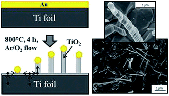
TiO2 nanowires (NWs) can improve the advantageous photocatalytic properties of TiO2 by increasing the active surface area. Here we investigate the synthesis of TiO2 NWs by thermal oxidation, studying the role of temperature, annealing time, and gas flow rates. The optimal thermal growth conditions were found to be 800 °C for 4 h in a mixed gas flow of Ar and O2. Morphological and structural characterizations, carried out by scanning and transmission electron microscopy, and X-ray diffraction, indicated a TiO2 rutile monocrystalline structure of the nanowires. An in situ thermal growth analysis was performed by means of an environmental electron microscope, providing additional insights into the TiO2 NWs growth dynamics. The photocatalytic properties were studied by using the degradation rate of methylene blue under UV light. TiO2 NWs revealed a 70% improvement of the degradation rate compared to a reference TiO2 bulk sample. Moreover, NWs were additionally annealed in forming gas (5% H2 in N2) in order to promote the formation of oxygen vacancies and an increase of the carrier density. Indeed, the photocatalytic activity of the NWs treated in forming gas was 3 times higher than that of the reference TiO2 bulk sample. The photonic efficiency and the quantum efficiency, also showed an increase versus bulk TiO2 of about 20% in the presence of NWs, and of about 100% with the forming gas annealing. Moreover, this increase in the photocatalytic activity after the forming gas annealing also correlates with the disappearance of a deep level recombination center as observed by deep level transient spectroscopy.


1. Introduction

Titanium dioxide or titania (TiO2) is a well known material of increased interest since the pioneering work of Fujishima and Honda in 1972,1 which demonstrated its advantageous photocatalytic properties. Titania is an earth abundant material with various advantageous features, such as optimal photo-catalytic properties, reasonable optical and electronic properties, long lifetime of excited electrons, non-toxicity, excellent long-term chemical stability, environmental safety, high corrosion resistance and relatively low cost.2–5 TiO2 is also widely applied in many sectors of industry like cosmetics, paints, food, and as a self-cleaning and whitening agent. On the other hand, its large band gap (∼3 eV) enables TiO2 to absorb only in an UV range of the solar spectrum. TiO2 has been used in a range of applications, while showing particular promise in photo catalysis, photovoltaic, chemical sensing, and optical devices.6 Specifically, in water purification, it is widely employed as it can prevent the proliferation of microorganisms and degrade organic compounds (e.g. bacteria and pharmaceutical pollutants) that are exposed to UV light. Nanowires can be used as building blocks of membranes and water filters.7,8 Moreover, the increased surface/volume ratio of nanostructures can also improve the degradation process being photocatalysis a surface process.

The focus of this paper is the study of the particular structures called nanowires (NWs) of TiO2, for applications in water purification. Literature reported several methods for the synthesis of TiO2 NWs such as hydrothermal process,9 chemical vapor deposition10 and thermal oxidation.11–14

In this work, we focus on the synthesis of NWs by seed assisted growth and thermal oxidation; Vapour–Liquid–Solid (VLS) and Vapor–Solid (VS) are reported as growth mechanisms for TiO2 NWs.11 Thermal methods allow producing TiO2 NWs with low chemical contaminations in the stable phase of rutile. Synthesis mechanism is still controversial and a systematic study as a function of annealing parameters is lacking. Moreover, NWs can be grown on a solid substrate offering the possibility to perform an experimental investigation of their electrical properties with conventional and well-established spectroscopic characterization techniques. Defects in TiO2 can affect the photocatalytic activity, so it is important to correlate the several properties of the material in a systematic framework of characterizations. In this work, we varied temperature, annealing duration, gas content and flow during the annealing in order to determine the process conditions, which optimize the NWs production in terms of NWs length, density and structure. Scanning Electron Microscopy (SEM) with in situ annealing helped to understand the transition between the growth of NWs and the concurrent micro-grain TiO2 structures as a function of temperature and time. The photocatalytic activity and the electrical properties of the NWs were also investigated by using the dye degradation method of methylene blue and Deep Level Transient Spectroscopy (DLTS), respectively. In particular, it has been reported15,16 that an atmosphere of H2 in N2 can increase the photoefficiency of TiO2 by the formation of oxygen vacancies, which increase the shallow donor density, promoting the conductivity and improving the charge collection. We used an additional annealing in forming gas (a mixture of H2 and N2 gas) in order to investigate the effect on the TiO2 electrical properties.

2. Experimental

Materials preparation

The samples used as substrate for the growth of TiO2 NWs were Ti foils, with thickness of 0.25 mm and purity ≥ 99.99% (Sigma Aldrich). Each sample was cut by diamond saw in pieces of about 1 × 1 cm2 and cleaned via ultra-sonication in acetone for 30 min and in isopropyl alcohol for 15 min. Afterwards, a thin layer of Au with thickness in the range of 3–5 nm, was deposited on the sample surface by means of an RF (60 Hz) Emitech K550X sputter. The deposition occurred in Ar flow at a plasma current of 10 mA for 1 to 3 min, with a chamber pressure of 0.02 mbar and using an Au target of 99.999% purity. Then, in order to synthesize the TiO2 NWs, the thermal oxidation process was applied by annealing in a carbolite horizontal furnace at temperatures between 700 °C and 1000 °C, for 1 to 4 hours in a mixed gas flow of argon (1.5–10 lpm) and oxygen (5–1 lpm). Some samples were additionally annealed in Forming Gas (FG, a mixture of nitrogen and hydrogen at 5%) at 500 °C for 2 h.

For the in situ thermal growth, an Au film was deposited on the Ti foil surface, following the same procedure already reported for the other samples. Then, the sample was inserted in the SEM furnace placed inside the SEM chamber and annealed at 1000 °C in water vapour atmosphere at 500 Pa. The in situ SEM annealing was performed using a FEI Quanta 200 FEG Environmental-SEM.

Characterization

The morphology was analysed by SEM using a Gemini field emission SUPRA 25 of Carl Zeiss, in plan-view and cross-section. The structure was investigated with X-Ray Diffraction (XRD) by means of a Bruker D-9000 diffractometer (wavelength Cu Kα). The Au thickness was determined by Rutherford Backscattering Spectrometry (RBS) with 2 MeV 4He+ beam and 165° scattering angle. Transmission Electron Microscopy (TEM) was performed by using a microscope Jeol 2010F with a camera Gatan Orius 2k/2k at an acceleration voltage of 200 keV.

For the electrical measurements, 100 nm thick Au contacts were deposited on the TiO2 NW samples and on a reference sample without NWs for comparison. The depositions were made by thermal evaporation through a shadow mask and the contacts displayed a Schottky behavior with about one order of magnitude (or more) in current rectification between +1 V in forward and −1 V in reverse bias. The DLTS measurements were carried out in the temperature interval of 50 to 300 K using a refined version of the setup described in ref. 17; the quiescent reverse bias used was −1 V together with 1 V filling pulse of 50 ms duration.

Photocatalytic experiment

The study of the photo-catalytic properties was carried out following the international standards ISO 10678:2010.18,19 We monitored the degradation of a common dye, the methylene blue (MB), in de-ionized water solution under UV light irradiation.

First, the sample was preconditioned: it was exposed to UV light (TL 8W BLB 1FM Philips lamp, in the wavelength range of 350–400 nm with a stable irradiance of 1.1 mW cm−2 at the sample surface) for 1 h, in order to clean the surface from any organic contaminant,20 which could affect the measurements. Then, the sample was placed in a cuvette filled with the MB water solution (2 ml at ∼10–5 M) and kept in dark. In this way the dye degradation was monitored in dark for about 12 h until saturation (variation <1% hour−1); after this step, the decrease of MB concentration due to the physical absorption of the dye by the sample surface can be considered negligible. Afterwards, the cuvette with the MB and the sample was covered with a quartz glass to prevent the solution evaporation, and irradiated with the same UV light employed for the preconditioning step; the experiment was carried out at standard room temperature conditions. Meanwhile, we monitored the MB degradation by measuring the absorbance of the solution at the wavelength of 664 nm, which is proportional to the MB concentration according to the Lambert–Beer law.21 During 3 hours we measured every 20 min the absorbance, by means of a spectrophotometer (Lambda45, Perking-Elmer) in the wavelength range of 500–750 nm. With these values, normalized to the macroscopic area, we could calculate the pseudo-first order photocatalytic rate constant or degradation rate of our sample, following the degradation kinetics law.22 Parallel measurements were performed with a reference control sample consisting of a cuvette of MB solution.

In addition, measurements of the samples' total reflectivity were carried out by means of a Lambda 40 Perking-Elmer spectrophotometer with integrating sphere, in order to evaluate the fraction of reflected photons.

3. Results and discussion

NWs synthesis on Ti foil

TiO2 NWs on Ti foil were synthetized using different annealing times (1 to 4 hours), temperatures (700 °C to 1000 °C) and flow rates (various O2/Ar mix). The effect of the annealing temperature was investigated by thermally processing the Au/Ti samples at 700 °C, 800 °C, 900 °C and 1000 °C. Below 700 °C we observed a poor growth of NWs (very few NWs in some small regions of the sample, not reproducible distribution).

Fig. 1 reports the SEM plan-view images of samples annealed at 700 °C (Fig. 1a and e), at 800 °C (Fig. 1b and f), at 900 °C (Fig. 1c and g) and at 1000 °C (Fig. 1d and h) in a flow of Ar (10 lpm) and O2 (7.5 lpm). The images in Fig. 1a to d refer to samples annealed for 1 hour, while 4 hours annealing was applied to the foils reported in Fig. 1e to h.


image file: c6ra09088e-f1.tif
Fig. 1 SEM plan view of TiO2 NWs growth at different temperatures: (a) and (e) at 700 °C, (b) and (f) at 800 °C, (c) and (g) at 900 °C, (d) and (h) at 1000 °C. Annealing time of 1 h was applied for the samples (a) to (d), and 4 h for samples (e) to (h).

At 700 °C very few NWs were grown, and they are characterised by a maximum length of 200–300 nm (Fig. 1a). At 800 °C (Fig. 1b) the NWs density increased and the maximum length went up to 2–3 μm. Au nanoparticles are present on top of the nanowires, indicating a mechanism of seed assisted growth23 that could be the VLS process, well-known in the literature particularly for the synthesis of silicon nanowires.24 This means that nanowires are formed because of the unidimensional growth that is catalysed by the Au nanoparticles laying on the surface. Since there are no upstream source of Ti, the Ti source should be the substrate itself. Ti diffusion up to the Au free surface and the formation of both anatase and rutile by reacting with oxygen, were reported to occur already at low temperature (<400 °C).25 In this case, since the Au layer is very thin (3–5 nm), Au forms nanoparticles because of de-wetting26 and catalyse the growth of nanowires with Ti provided from the substrate (see the schematic representation in Fig. 2). The driving force for NWs growth is the diffusion of Ti from the substrate, this can be due to a local gradient of chemical potential due to the presence of Au particles. Once the catalytic particles are formed the growth of nanowires is associated with a steady state growth in which material is transported to the particle/nanowire interface. The role of the Au catalyst is crucial since a preferential nucleation at the interface Au/Ti substrate occurs while nucleation on others is suppressed.27 Being in oxygen atmosphere, TiO2 formed and the TiO2 nanowire elongated along a main growth direction. Ti diffusion from the substrate is also indicated by the tapering shape of the NWs which have a wider base.


image file: c6ra09088e-f2.tif
Fig. 2 Schematic representation of TiO2 nanowires growth. First, a thin Au layer (3–5 nm) is deposited on the Ti foil substrate. After, the annealing process Au nanoparticles form because of de-wetting and catalyse the growth of TiO2 nanowires with the Ti provided from the substrate and O from the atmosphere.

Furthermore, several nanowires present a change of direction within their structures, even with very sharp edges. This effect is probably due to the presence of an extended defect in the crystallographic structure of the nanowire. Indeed, as for a polycrystalline growth,28 the nucleation of a crystallographic defect can act as an instability and lead to an abrupt change of crystal structure that – in the nanowire – is observed like a sharp change of the main growth direction.

Increasing the annealing temperature to 900 °C (Fig. 1c), the synthetized structures stay very similar to the ones processed at 800 °C. An increase of the average length of the NWs up to 4–5 μm is just observed.

A different effect was obtained by annealing at 1000 °C, where the NWs growth mechanism occurred in competition with microcrystal grain formation, as showed in the SEM image of Fig. 1d.

It is important to mention that the samples processed at annealing temperatures higher than 800 °C, resulted to be fragile and friable at the macroscopic level.

Fig. 1e to h show the samples obtained after increasing the annealing time to 4 hours. In particular, a comparison of Fig. 1a and e show that at 700 °C the nucleation is improved (higher density of NWs) together with the length and the diameter of the nanostructures. At 800° and 900 °C we observe an increase in the average NWs length. This is due to the fact that the nucleation is fully activated at temperatures higher than 700 °C, therefore longer annealing time only favour the growth of NWs in length. Fig. 1h (sample processed at 1000 °C, 4 h) shows that the competitive micro-grains nucleation prevails over the NWs growth, since the grains increased in size while the NWs are shorter and set on the top of the grains. In the following, mainly the Ti foil annealed at 800 °C for 4 hours is studied, as it is considered the optimal sample.

The growth direction of nanowires has no specific orientation with respect to the substrate. Epitaxial growth was observed for Si VLS nanowires on a single crystal substrate.24 This is not the case for Ti, since the substrate foil has a polycrystalline structure.

Several nanostructures are formed during the annealing process. The SEM plan-view images of Fig. 3 show that it is possible to find structures such as ribbons, facet nanowires, spikes, rods, either with or without the Au cap on the top. However, the predominant structure is the facet nanowire with gold on its tip, as also illustrated by the images in Fig. 1. In Fig. 3c and d, it is also possible to better appreciate the morphology of the NWs Au caps, which do not show a spherical shape but a facet one. If this means that Au is more a solid than a liquid catalyst is still under debate and both phases showed to catalyse NWs growth.29


image file: c6ra09088e-f3.tif
Fig. 3 SEM plan view of different TiO2 nanostructures grown during the thermal oxidation process of a Ti foil. Synthesis conditions: 700 °C 4 h (a) and (b); 800 °C 4 h (c); 900 °C 4 h (d).

In order to investigate the nucleation mechanism in relation to the different synthesis parameters, such as gas carrier flow and oxygen content, we prepared a set of samples processed with different gas flow in the furnace chamber at the annealing temperature of 700 °C, which is the threshold temperature for the activation of the nucleation process. Fig. 4a shows the high resolution SEM plan-view images of the annealed sample for 4 h at low Ar flow (1 lpm). The Ar gas used for this experiment was pure at 99.999%, so the oxygen contamination is negligible within the range of the experimental set up. TiO2 grains are well distinguished on the sample surface and some of them have an elongated shape on their top that indicates the formation of a NW with a large base (inset of Fig. 4a). Au nanoparticles are well separated from each other, indicating that de-wetting occurred. Some Au nanoparticles appear to evolve in a dendritic shape as shown in the SEM image of the inset of Fig. 4a. This effect was reported for Au de-wetting on oxide substrate and it is related to the fast temperature quenching of the annealing process.30 NWs appear only in few spot with very small area (∼μm2). In particular, these few NWs nucleated without the seeds since the Au nanoparticles are not visible on the top. This kind of growth mechanism was reported in the literature for other metal oxides NWs, and it is promoted by the presence of surface roughness or defects in the substrate.31 Since the substrate is a Ti foil, this growth mechanism is randomly induced on the surface. The uniformity of NWs over the full sample area was indeed very poor in this condition, since NWs can only be detected in small bunches as the one shown in Fig. 4a. In Fig. 4b, it can be observed that the increase of Ar flow (to 15 lpm) favours the NWs growth in some larger spots of the sample with respect to the low gas flow condition (Fig. 4a). However, the distribution over the full sample area is still poor, as observed in the insert of Fig. 4b, where the bright zones contain NWs. Therefore, we investigated how to improve a uniform density distribution of NWs. We observed that an increase of oxygen content was effective to promote a uniform growth. Fig. 5(a)–(c) report the SEM images of samples annealed at 700 °C for 1 h with different mix of argon and oxygen flow. The NWs distribution is uniform over the full size of the sample (Fig. 5d). However, the effect of Ar/O2 ratio in this range of gas flow does not provide a remarkable effect in terms of NWs density increase. The optimal gas condition was then set to 7.5 lpm of oxygen and 10 lpm of argon, based on the experimental reproducibility of results.


image file: c6ra09088e-f4.tif
Fig. 4 SEM plan view of TiO2 foil with a 3 nm of gold layer deposited on the surface, annealed at 700 °C for 4 h with (a) a low Ar flow of 1 lpm and (b) an high Ar flow of 15 lpm. Bright zones in the insert of (b) contain NWs.

image file: c6ra09088e-f5.tif
Fig. 5 SEM plan views of TiO2 samples annealed at 700 °C for 1 h with different argon and oxygen flows: (a) O2 1.5 lpm and Ar 10 lpm; (b) O2 5 lpm and Ar 10 lpm; (c) O2 10 lpm and Ar 5 lpm; (d) O2 7.5 lpm and Ar 10 lpm (optimal flow) view at low magnification.

The structure of the TiO2 NWs was analysed by XRD and the results are shown in Fig. 6. The TiO2 signals are always found to be rutile phase, which is reported to be the most stable structure upon annealing at temperatures higher than 600 °C.32 The most intense peak is represented by the (110) orientation that is reported to be the most thermodynamically stable in the rutile TiO2 structure.2 The signals associated to gold are also present, and they are due to the Au nanoparticles localized on top of the NWs.


image file: c6ra09088e-f6.tif
Fig. 6 XRD analysis of TiO2 NWs synthetized by thermal oxidation at 800 °C for 4 h under a flow of O2 7.5 lpm and Ar 10 lpm.

Fig. 7a shows the TEM image of a single NW, removed from the substrate. The NW has a quite uniform diameter equal to about 200 nm, which shrinks in the top third part down to about 120 nm. The corresponding diffraction pattern reported in the inset indicates that the NW is a pure rutile TiO2 monocrystalline. Indeed, it is oriented along the 〈110〉 direction as demonstrated by the diffraction pattern, in the 〈1−12〉 zone axis. Moreover, from the high resolution TEM shown in Fig. 7b, the crystal planes are clearly distinguishable. The corresponding fast Fourier transform is reported in the inset and it confirms that the NW growth direction corresponds to the 〈110〉 direction.


image file: c6ra09088e-f7.tif
Fig. 7 (a) TEM image of a single NW and its diffraction pattern (inset); (b) high resolution TEM of the NW and the corresponding fast Fourier transform (inset).

In situ thermal growth

In order to investigate in more detail the evolution of NWs since nucleation to growth, an in situ thermal growth was performed by means of an environmental SEM on a Ti foil substrate, coated with Au thin film, as described in Section 2. The sample was inserted in the SEM furnace placed inside the SEM chamber and annealed at 1000 °C in water vapour atmosphere at 500 Pa. The water vapor atmosphere is the most similar environment condition that can imitate the furnace experiment. The SEM detector showed that as soon as we started the annealing, an explosive growth of NWs occurred (length of about ∼30 μm) at the sample surface. The main growth occurred during this initial stage and Fig. 8 reports a representative SEM plan view of the sample after about 30 min annealing.
image file: c6ra09088e-f8.tif
Fig. 8 SEM plan view images of TiO2 NWs synthetised by in situ thermal growth at 1000 °C in water vapour atmosphere at 500 Pa, at an annealing time of about 30 min.

Applying a lower annealing temperature of 800 °C with the same conditions of atmosphere and pressure, the growth process is slower and the NWs growth dynamics was monitored as a function of time. It was possible to obtain SEM images on every 2 minutes for a total annealing time of 2 hours and 15 minutes (in situ Video available as ESI). Fig. 9 reports six representative images of a sample area near the edge, obtained when the annealing was just started (Fig. 9a), and then after different annealing times, i.e. 20 min (Fig. 9b), 40 min (Fig. 9c), 1 h (Fig. 9d), 1 h 45 min (Fig. 9e) and 2 h 15 min (Fig. 9f). During the first 20–40 minutes (Fig. 9b and c), there is higher rate of growth of NWs in length and density, with dimension up to 10–20 μm in length and up to ∼102 nm in diameter. During the following hour (Fig. 9d and e), the NWs tend to shorten and become wider in their base, creating more wide rods/grains shapes, with width and length both of a few microns.


image file: c6ra09088e-f9.tif
Fig. 9 SEM plan view images of TiO2 NWs synthetized by in situ thermal growth at 800 °C in water vapour atmosphere at 500 Pa, at the beginning of the annealing (a) and after an annealing time of 20 min (b), 40 min (c), 1 h (d), 1 h 45 min (e) and 2 h 15 min (f).

This is in agreement with the study of Perez33 that reports an increased oxidation rate of Ti for short times in water vapour; while, as the annealing time increases, the oxidation rate decreases and the formation of dense oxide scales is observed. Motte et al.34 also reported an higher oxidation rate of Ti for short time of annealing under water vapour.

Althought the experimental conditions of in situ annealing are slightly different with respect of furnace treatments, the in situ experiment allows to detect the critical steps of nanowires nucleation (early stage of annealing) and that of the concurrent nucleation of microcrystals as a function of annealing time, indicating a very complex dynamics of growth.

Optical properties

The total reflectance spectra (%) of the three studied samples were measured and reported in Fig. 10, together with the spectrum of the UV lamp employed for the photocatalytic measurements. The reported samples are: foil with TiO2 NWs, foil with TiO2 NWs and additional annealing in forming gas at 500 °C for 2 h and, TiO2 bulk reference sample without NWs. The spectra of both TiO2 NWs samples present a clear reduction in reflectivity for wavelengths below 400 nm compared to bulk TiO2 sample, note that the UV lamp spectrum locates in this spectral range. Since both TiO2 NWs samples present similar nanostructures but different annealing process the observed antireflective effect can be directly associated mainly to the nanostructure.35
image file: c6ra09088e-f10.tif
Fig. 10 Reflectance of the three studied samples and spectra of the employed UV lamp.

Photocatalytic properties

The photo-catalytic activity of the synthetized NWs is illustrated in Fig. 11. The plot shows the values of the logarithm of the absorbance at 664 nm normalized to the initial value at t = 0 s (after preconditioning step) and to the macroscopic area of each sample; the lines represent the fits with linear regression. The reported data refers to the following samples: MB reference solution without any TiO2 sample (blue downward triangles); TiO2 reference sample without NWs (green upward triangles); foil with TiO2 NWs (black squares); foil with TiO2 NWs and additional annealing in forming gas at 500 °C for 2 h (red circles). The TiO2 reference sample is a Ti foil without gold that was processed with the same annealing treatment as the NWs sample, so it has rutile TiO2 micro-grains, like the ones observed on the NWs background (see Fig. 1). The negative slope of the lines (not considering the MB reference solution), confirm a decrease with time of the absorbance and therefore of the MB concentration; this indicates that the TiO2 photocatalysis reaction, i.e. the degradation of the dye, took place. This slope represents the pseudo-first order photocatalytic rate constant (or degradation rate) of the photo-catalysis reaction per unit of area. The inset of Fig. 11 shows more clearly the degradation rate (K) of the samples per unit area (A) normalised to the degradation rate of the TiO2 reference sample without NWs. The histogram illustrates that the sample with TiO2 NWs shows an increase in the degradation rate of almost 70% compared to the one of the reference TiO2 foil without NWs. Moreover, an additional thermal treatment in forming gas resulted in a further improvement of the degradation rate, which is almost 3 times higher compared to the one of the reference TiO2 foil and almost doubled versus the one of the TiO2 NWs sample. These results indicate that the presence of NWs gives a considerable contribution to the photocatalytic properties of the material. Furthermore, they suggest that the annealing in H2 atmosphere acted on the TiO2 NWs sample increasing the carrier density15,16 and so the surface degradation reactions.
image file: c6ra09088e-f11.tif
Fig. 11 Photocatalytic activity of various samples: MB reference solution without any TiO2 sample (blue downward triangles); TiO2 reference foil without NWs (green upward triangles); TiO2 foil with NWs (black squares); TiO2 foil with NWs and additional annealing in forming gas (FG, red circles). Inset: degradation rate per unit area (K/A) of the samples normalised to the K/A obtained from the TiO2 reference foil without NWs.

The mean photonic efficiency of the MB degradation (ζMB) was calculated as indicated in the international standards ISO 10678:2010:18

 
image file: c6ra09088e-t1.tif(1)
where PMB is the photoactivity, corresponding to the average degradation rate of MB calculated during the UV irradiation (mol s−1) per unit of area; EP is the mean photon UV-radiation intensity from the lamp used during the MB experiment (mol s−1 of photons with a wavelength of 368 nm). ζMB refers to the efficiency of the photons in the process of MB degradation, considering the total light incident on the sample (also knows in literature as apparent photonic efficiency). The resulting efficiencies for the three samples are reported in Table 1. The NWs sample showed an increased photon efficiency of 25% compared to the TiO2 sample without NWs. Moreover, the NWs annealed in forming gas, revealed an even higher photon efficiency, doubled with respect to the ζMB of the reference TiO2 foil. Another significant parameter to understand the efficiency of the materials is the quantum efficiency of the system in the MB degradation (ΦMB), which considers only the effect of the absorbed (or not reflected) photons.36

Table 1 Photocatalytic and efficiency parameters of the studied samples
  TiO2 (no NWs) TiO2 NWs TiO2 NWs + FG
K/A [a.u] 1 1.67 2.98
ζMB [%] 0.0095 ± 0.0009 0.012 ± 0.001 0.019 ± 0.001
ΦMB [%] 0.011 ± 0.001 0.013 ± 0.001 0.021 ± 0.001


The quantum efficiencies were then calculated by using the values of reflectance in the range of the spectra of the UV lamp used in our MB experiment (Table 1). The obtained ΦMB values for the as obtained NWs sample showed similar values to that of reference TiO2 foil. Thus, the NWs nanostructure contributes to the observed enhancement in photocatalytic activity by improving the photon harvesting (antireflective effect); however, ΦMB values of NWs treated in the FG increase went up to 90% compared to reference TiO2. Therefore, the treatment in forming gas provides an additional intrinsic modification in the NWs characteristics.

Electrical properties by deep level transient spectroscopy

Fig. 12 shows DLTS spectra of two TiO2 NW samples, one as-grown at 800 °C (4 h in a flow of Ar 10 lpm and O2 7.5 lpm) and one subjected to post-growth treatment in FG at 500 °C similar to that for the samples in Fig. 10. Further, the spectrum of an as-grown TiO2 sample without NWs is also included for comparison. Four peaks are clearly resolved occurring at ∼55 K, ∼110 K, ∼188 K and >320 K, respectively, and they are labelled E1, E2, E3 and E4. The E4 peak was not possible to cover fully because of the high conductance of the Schottky contacts at temperatures above 320 K. The corresponding energy positions extracted from six DLTS spectra, recorded simultaneously during one temperature scan and with rate windows between (20 ms)−1 and (640 ms)−1, are given in Table 2. The apparent electron capture cross sections of the levels, obtained by extrapolation of the Arrhenius plots of their emission rates, are also included in Table 2. The spectra of the ‘no NW sample’ and the as-grown ‘NW sample’ are similar both in shape and amplitude of the four peaks. However, the ‘NW + FG sample’ exhibits a considerably higher amplitude of the shallow E1 peak than the other samples while the E2, E3 and E4 peaks are substantially weaker.
image file: c6ra09088e-f12.tif
Fig. 12 DLTS spectra between 50 and 325 K for three different samples; ‘TiO2 NW’ (as grown), ‘TiO2 NWs + FG’ (annealed at 500 °C in FG), and a TiO2 sample without NWs. Reverse bias = −1 V, filling pulse = +1 V, and rate window = (640 ms)−1.
Table 2 Energy level positions and apparent electron capture cross sections of the E1, E2, E3 and E4 levels
Level ECET [eV] σ [cm2]
E1 0.11 ∼10−14
E2 0.30 ∼10−13
E3 0.45 ∼10−14
E4 >0.6


This holds especially for the deep E4 peak which has vanished and the spectrum displays negative values above ∼275 K presumably caused by hole injection. The loss of the E4 level after the FG treatment can be correlated with the increase in photocatalytic activity of the ‘NW + FG’ sample in Fig. 9. As mentioned above, the position of the E4 level cannot be determined from the present data but it is estimated to be located at least 0.6 eV below EC assuming a capture cross section with a typical value of ∼10−15 cm2. Hence, E4 can be anticipated to act as a competing charge carrier recombination center suppressing the catalytic effect of the photon-induced electron–hole pairs.

The identity of the E1, E2, E3 and E4 levels is not known and previous DLTS data in the literature on deep levels in TiO2 NWs are scarce (if any). In fact, this holds also for mono-crystalline TiO2 bulk material where the recent amount of DLTS reports is very limited. An early study by Duckworth et al.37 showed the presence of a level at ∼EC-0.4 eV in Nb-doped rutile samples. This level is possibly identical to the E3 level in our samples, and Duckworth et al. discussed a tentative assignment to the oxygen vacancy. Regarding the E4 level, it is tempting to make an association with a defect of dangling bond character being passivated by hydrogen during the FG annealing. However, further work needs to be pursued in order to confirm this speculation.

4. Conclusions

Thermal oxidation synthesis of TiO2 NWs was performed on substrates of Ti foils coated with a thin layer of Au (3–5 nm). Annealing at temperature below 700 °C for 1 h revealed very rare and short NWs. With increasing temperature, the NWs grew in length and in density. At 1000 °C, a mechanism of micrograins growth appeared in competition with the NWs evolution. Increasing the annealing time up to 4 h amplified the effect obtained for 1 h. Besides, the samples annealed at temperature higher than 800 °C became macroscopically friable. Hence, the optimal growth parameters were set at 800 °C and 4 h. Concerning the annealing atmosphere, an increase in gas flow rates improved the nanowires coverage, while varying the mixture of Ar and O2 did not give relevant changes. The optimal gas condition was 7.5 lpm of oxygen and 10 lpm of argon. XRD measurements of the NWs revealed a TiO2 rutile crystalline phase with a main peak from the (110) orientation. TEM analysis indicated that the NWs are pure TiO2 monocrystalline and that the NW growth direction corresponds to the 110 direction. In situ thermal growth in water vapor atmosphere at 800 °C for about 2 h, showed that the rate of NWs growth in length and density was higher in the first 20–40 minutes (length up to 10–20 μm); subsequently the oxidation rate decreased and the NWs tent to shorten and became wider in their base, creating more wide rods/grains shapes (length of few μm).

The analysis of the photocatalytic properties of the TiO2 NWs showed a degradation rate 70% higher compared to the one of a reference TiO2 bulk sample. The photocatalytic activity of the NWs treated with forming gas, was 3 times higher than that of the reference bulk TiO2 sample. According to DLTS measurements of the NW samples, the annealing in forming gas leads to a reduction of deep level recombination centers competing with the photocatalytic processes. These increases in efficiency indicate the positive contribution of the NW structures, via antireflective effect and of the additional forming gas treatment, to the photocatalytic activity of TiO2. These results are, indeed, promising for applications of TiO2 where nanowires are required, like for examples photocatalytic membranes or filters.

Acknowledgements

This research has been supported by the FP7 European Project WATER – Winning Applications of nanoTEchnologies for Resolutive hydropurification (Grant Agreement No. 316082). The authors wish to thank Mr Salvo Tatì (CNR-IMM), Mr Carmelo Percolla (CNR-IMM) and Mr Giuseppe Pantè (CNR-IMM) for technical support and Dr Nahum Masó Carcasés (University of Oslo) for his precious technical help during the SEM in situ analysis. The authors are also grateful to the Research Council of Norway and University of Oslo for partial financial support.

References

  1. A. Fujishima and K. Honda, Nature, 1972, 238, 37 CrossRef CAS PubMed.
  2. A. Fujishima, X. Zhang and D. A. Tryk, Surf. Sci. Rep., 2008, 63, 515 CrossRef CAS.
  3. X. Chen and S. S. Mao, Chem. Rev., 2007, 107, 2891 CrossRef CAS PubMed.
  4. V. Scuderi, G. Impellizzeri, L. Romano, M. Scuderi, M. V. Brundo, K. Bergum, M. Zimbone, R. Sanz, M. A. Buccheri, F. Simone, G. Nicotra, B. G. Svensson, M. G. Grimaldi and V. Privitera, Nanoscale, 2014, 6, 11189 RSC.
  5. V. Scuderi, G. Impellizzeri, L. Romano, M. Scuderi, G. Nicotra, K. Bergum, A. Irrera, B. G. Svensson and V. Privitera, Nanoscale Res. Lett., 2014, 9, 458 CrossRef PubMed.
  6. W. Y. Teoh, J. A. Scott and R. Amal, J. Phys. Chem. Lett., 2012, 3, 629 CrossRef CAS PubMed.
  7. X. Zhang, T. Zhang, J. Ng and D. D. Sun, Adv. Funct. Mater., 2009, 19, 3731 CrossRef CAS.
  8. A. Hu, X. Zhang, K. D. Oakes, P. Peng, Y. N. Zhou and M. R. Servos, J. Hazard. Mater., 2011, 189, 278 CrossRef CAS PubMed.
  9. H. Yin, G. Ding, B. Gao, F. Huang, X. Xie and M. Jiang, Mater. Res. Bull., 2012, 47, 3124 CrossRef CAS.
  10. J. Baik, H. M. Kim, C. Larson, X. Chen, S. Guo, A. M. Wodtke and M. Moskovits, Appl. Phys. Lett., 2008, 92, 242111 CrossRef.
  11. B. Dinan and S. A. Akbar, Funct. Mater. Lett., 2009, 2, 87 CrossRef CAS.
  12. J. M. Wu, W. T. Wu and H. C. Shih, J. Electrochem. Soc., 2005, 152, G613 CrossRef CAS.
  13. J. C. Lee, K. S. Park, T.-G. Kim, H.-J. Choi and Y.-M. Sung, Nanotechnology, 2006, 17, 4317 CrossRef CAS.
  14. B. Dinan, D. Gallego-Perez, H. Lee, D. Hansford and S. A. Akbar, Ceram. Int., 2013, 39, 5949 CrossRef CAS.
  15. C. Fàbrega, T. Andreu, F. Guell, J. D. Prades, S. Estradé, J. M. Rebled, F. Peirò and J. R. Morante, Nanotechnology, 2011, 22, 235403 CrossRef PubMed.
  16. G. Wang, H. Wang, Y. Ling, Y. Tang, X. Yang, R. C. Fitzmorris, C. Wang, J. Z. Zhang and Y. Li, Nano Lett., 2011, 11, 3026 CrossRef CAS PubMed.
  17. B. G. Svensson, K. H. Rydén and B. M. S. Lewerentz, J. Appl. Phys., 1989, 66, 1699 CrossRef CAS.
  18. Technical Committee ISO/TC 206, Fine ceramics (advanced ceramics, advanced technical ceramics) — Determination of photocatalytic activity of surfaces in an aqueous medium by degradation of methylene blue. ISO 10678:2010(E), International Organization for Standardization, Switzerland, 1st edn, 2010 Search PubMed.
  19. A. Mills, C. Hill and P. K. J. Robertson, J. Photochem. Photobiol., A, 2012, 237, 7 Search PubMed.
  20. R. Wang, K. Hashimoto, A. Fujishima, M. Chikuni, E. Kojima, A. Kitamura, M. Shimohigoshi and T. Watanabe, Nature, 1997, 388, 431 CrossRef CAS.
  21. A. D. McNaught and A. Wilkinson, Compendium of Chemical Terminology, Blackwell, Oxford, 2nd edn, 1997 Search PubMed.
  22. B. Ohtani, Chem. Lett., 2008, 37, 217 CrossRef CAS.
  23. K. W. Kolasinski, Curr. Opin. Solid State Mater. Sci., 2006, 10, 182 CrossRef CAS.
  24. R. S. Wagner and W. C. Ellis, Appl. Phys. Lett., 1964, 4, 89 CrossRef CAS.
  25. W. E. Martinez, G. Gregori and T. Mates, Thin Solid Films, 2010, 518, 2585 CrossRef CAS.
  26. C. V. Thompson, Annu. Rev. Mater. Res., 2012, 42, 399 CrossRef CAS.
  27. B. A. Wacaser, K. A. Dick, J. Johansson, M. T. Borgstrom, K. Deppert and L. Samuelson, Adv. Mater., 2009, 21, 153 CrossRef CAS.
  28. L. Romano, V. Privitera and C. Jagadish, Defects in Semiconductors, Multi-volume: Semiconductors and Semimetal, Elsevier, 1st edn, 2015 Search PubMed.
  29. V. Schmidt and U. Gösele, Science, 2007, 316, 698 CrossRef CAS PubMed.
  30. F. Ruffino, L. Romano, G. Pitruzzello and M. G. Grimaldi, Appl. Phys. Lett., 2012, 100, 053102 CrossRef.
  31. M. Chen, Y. Yue and Y. Ju, J. Appl. Phys., 2012, 111, 104305 CrossRef.
  32. D. A. H. Hanaor and C. C. Sorrell, J. Mater. Sci., 2011, 46, 855 CrossRef CAS.
  33. P. Perez, Corros. Sci., 2007, 49, 1172 CrossRef CAS.
  34. F. Motte, C. Coddet, P. Sarrazin, M. Azzopardi and J. Besson, Oxid. Met., 1976, 10, 113 CrossRef CAS.
  35. R. Sanz, L. Romano, M. Zimbone, M. A. Buccheri, V. Scuderi, G. Impellizzeri, M. Scuderi, G. Nicotra, J. Jensen and V. Privitera, J. Appl. Phys., 2015, 111, 074903 CrossRef.
  36. N. Serpone and A. Salinaro, Pure Appl. Chem., 1999, 71, 303 CrossRef CAS.
  37. C. N. Duckworth, A. W. Brinkman and J. Woods, Phys. Status Solidi A, 1983, 75, K99 CrossRef CAS.

Footnote

Electronic supplementary information (ESI) available. See DOI: 10.1039/c6ra09088e

This journal is © The Royal Society of Chemistry 2016
Click here to see how this site uses Cookies. View our privacy policy here.