
Diffusion kinetics of gold in TiO2 nanotube arrays for formation of Au@TiO2 nanotube arrays†
Wanggang Zhangabc,
Yiming Liuab,
Diaoyu Zhouab,
Jing Wenab,
Liuwei Zhengab,
Wei Liang*ab and
Fuqian Yang*ac
aCollege of Materials Science and Engineering, Taiyuan University of Technology, Taiyuan, Shanxi 030024, China. E-mail: liangwei@tyut.edu.cn
bKey Laboratory of Interface Science and Engineering in Advanced Materials, Taiyuan University of Technology, Ministry of Education, Taiyuan, Shanxi 030024, China
cDepartment of Chemical and Materials Engineering, University of Kentucky, Lexington, KY 40506, USA. E-mail: fyang2@uky.edu
First published on 11th May 2016
Abstract
A simple approach is presented to form Au@TiO2 nanotube arrays. This approach consists of the formation of pure TiO2 nanotube arrays by a two-step anodization process, the coating of a Au nanofilm on the top of the pure TiO2 nanotube arrays, and the heat treatment of the TiO2 nanotube arrays coated with the Au nanofilm. The heat treatment leads to the diffusion of Au atoms into the TiO2 nanotube arrays, resulting in the formation of Au nanocrystals on the outer surface of the TiO2 nanotubes. X-ray diffraction, field emission scanning electron microscopy, and transmission electron microscopy are used to characterize the microstructural evolution of the Au@TiO2 nanotube arrays, which reveals the phase change of TiO2 from amorphous phase to anatase phase. The kinetics of the migration of Au atoms into the TiO2 nanotube arrays is studied. The diffusivity for the diffusion of Au atoms on the outer surface of the TiO2 nanotubes is in the range of 4.14–19.4 × 10⁻¹⁸ m2 s−1 for temperature in the range of 400–500 °C. The activation energy for the migration/diffusion of Au on the outer surface of the TiO2 nanotubes in the temperature range of 400 to 500 °C is 67.2 kJ mol−1. The growth of Au nanocrystals on the surface of the TiO2 nanotubes can be described as a first order reaction.
1. Introduction
Embedding metallic particles or films in oxide nanotubes and nanowires/nanorods has attracted great interest due to the importance of metal-in-oxide systems in various applications, such as heterogeneous catalysis,1–7 photonics,8–10 and energy storage.11–18 Understanding the fundamental processes controlling the formation of metallic particles or films in oxide nanotubes and nanowires/nanorods and their correlation to the physicochemical properties of the metal-in-oxide systems can lead to the improvement in the design and processing of low-dimensional oxide structures with metallic particles or films and in the tailoring of intriguing physicochemical properties as a function of particle size (film thickness), shape and interfacial interaction.There are various methods for the formation of metallic particles in oxide nanotubes and nanowires/nanorods, including sputtering,19 electrodeposition,20–22 irradiation of microwave,23 photo irradiation,24 reduction,25 dipping-deposition,26 and sol–gel process.27 Yoo et al.26 used the dipping-deposition process to precipitate Au nanoparticles on the outer surface of TiO2 nanotubes. Xin et al.22 used electrochemical-induced self-doping process to decorate Au nanoparticles on functionalized, self-doped TiO2 nanotubes. Xiao28 used electric interaction between positively charged TiO2 nanotubes and negatively charged, dithiolated DTDTPA (diethylenetriaminepentaacetic) linkers to construct heterostructures, leading to the formation of monodisperse Au nanoparticles on the surface of TiO2. It is known that one can deposit a metallic film on the surface of nonconductive substrates, using sputtering techniques, which avoid the use of aqueous solution. Yoo et al.19 used plasma sputtering deposition and dewetting (heat treatment) processes to form Au nanoparticles on the surface of TiO2 nanotubes of ∼80 nm in diameter and ∼200 nm in length. They observed that Au nanoparticles were present near the bottom of the TiO2 nanotubes. Using RF magnetron sputtering and heat treatment, Lu et al.29 prepared Au nanoparticle-decorated TiO2 nanotube arrays and found that Au nanoparticles were dispersed within the wall and on the surface of the TiO2 nanotubes. However, both did not study the kinetic process of the migration/diffusion of Au atoms, which plays an important role in controlling the microstructures of Au@TiO2 nanotubes.
A primary objective of the current study is to synthesize Au@TiO2 nanotube arrays with controllable, reproducible morphologies for the applications in heterogeneous catalysis and energy storage. A method is presented to produce Au@TiO2 nanotube arrays via magnetron sputtering and heat treatment. The heat treatment not only leads to the transformation of TiO2 nanotube arrays from amorphous phase to anatase phase but also results in the diffusion of Au atoms. The microstructures of the Au@TiO2 nanotube arrays are characterized, and the diffusivity and activation energy for the diffusion of Au atoms on the surface of TiO2 nanotubes are determined. The growth behavior of Au nanoparticles on the surface of TiO2 nanotubes is also discussed.
2. Experimental detail
Preparation of TiO2 nanotube arrays
Scheme 1 schematically shows the facile route of preparing Au@TiO2 nanotube arrays. TiO2 nanotubes on Ti substrates were fabricated by following a two-step anodization process.30,31 Commercial pure titanium sheets of 30 × 10 × 0.1 mm3 (China Research Institute of Nonferrous Metals, China) were degreased first by ultrasonic cleaning successively in acetone, ethanol, and deionized water, then rinsed with deionized water, and finally dried at room temperature. The anodization of the titanium sheets was performed in a two-electrode configuration with the Ti sheet as the working electrode and a platinum sheet as the counter electrode with constant voltage at room temperature (25 °C). The distance between the working electrode and the counter electrode during anodization was 2 cm. The anodization voltage was 50 V. After being anodized for 1 hour, the as-anodized Ti sheets were ultrasonically cleaned to remove the surface layer containing the nanotubes formed in the anodization. The Ti foils were then cleaned ultrasonically again, and were anodized for another 30 min under the same condition to obtain pure TiO2 nanotube arrays. After the anodization, the Ti sheets with TiO2 nanotube arrays were ultrasonically cleaned in deionized water to remove surface debris, and dried at room temperature. Fig. S1† shows the outer surfaces of the TiO2 nanotubes prepared by the one-step anodization process and the two-step anodization process, respectively. | ||
| Scheme 1 Schematic of the facile route for the preparation of Au@TiO2 nanotubes; (a) Ti sheet, (b) TiO2 nanotubes formed after the first anodization, (c) imprints left on the surface of the Ti sheet after ultrasonication, (d) TiO2 nanotubes formed after the second anodization, (e) Au nanofilm deposited on the top of the TiO2 nanotube arrays via magnetron sputtering, and (f) Au@TiO2 nanotube arrays. | ||
The deposition of an Au nanofilm on the top of the pure TiO2 nanotube arrays was performed at room temperature (25 °C) by magnetron sputtering in a multifunctional magnetron sputtering instrument (JGP560B) under the condition of high vacuum, using an Au target. Argon gas was flowed into the sputtering chamber after the pressure of the sputtering chamber reached 8 × 10⁻⁴ Pa. Pre-sputtering of 3 min was performed to remove surface residuals. During the sputtering, the flow rate of argon gas was 30 sccm, and the chamber pressure was 6 Pa. The distance between the Ti sheet and the target was 30 mm. The loading amount of Au, i.e. the thickness of an Au nanofilm, was controlled by the sputtering time. The thicknesses of the prepared Au nanofilms were also measured by scanning electron microscopy.
The TiO2 nanotube arrays with Au nanofilm were heat-treated at three different temperatures of 400, 450 and 500 °C for three different heating times of 1, 3 and 5 h at a ramping rate of 2 °C min−1 in a tube furnace in air. The TiO2 nanotube arrays with Au nanofilm were also heat-treated in argon gas at 450 °C for 3 h.
Materials characterization
The surface topology of the prepared nanotube arrays was characterized by Transmission Electron Microscopy (TEM) (JEOL 2100 F) at 200 kV and Field Emission Scanning Electron Microscopy (FESEM) (Tescan MIRA3 LMH) at 10 kV. The composition of the nanotubes was determined using Energy Dispersive Spectroscopy (EDS) (OXFORD X-Max 20). The crystal structure of the nanotubes was analyzed with the Cu Kα line on a Rigaku D/max 2500 X-ray diffractometer with patterns recorded in a range of 20–80°. The binding energy was determined, using X-ray photoelectron spectroscopy (XPS) (Escalab 250).3. Results
Fig. 1 shows the XRD patterns of the prepared pure TiO2 nanotubes and TiO2 nanotubes with Au nanofilm after heat treatment at different temperatures for different heating times. There are diffraction peaks with 2θ values of 25.3°, 37.8°, 48.0°, and 54.0°, corresponding to the (101), (004), (200), and (105) crystal planes of anatase TiO2. These results are consistent with the values in the standard card (JCPDS no. 21-1272). There is no peak detectable for rutile TiO2. It is evident that the heat treatment in the temperature range of 400 to 500 °C caused the transform of amorphous TiO2 to anatase TiO2 in the TiO2 nanotubes with Au nanofilm. This result is in accord with the reports by Ismail et al.32 in the calcination of Au/TiO2 nanoparticles at 500 °C and Xiao7 in the preparation of Au/TiO2 nanotube heterostructures with the heat treatment at 450 °C in air and in contrast to the results given by Yoo et al.19 Yoo et al.19 found that the heat treatment of the TiO2 nanotubes at 450 °C for 30 min led to the transform of amorphous TiO2 to a mixture of anatase and rutile TiO2. The mechanism for such a difference is unclear. It might be associated with the use of different aqueous solutions. Yoo et al.19 used a HF/H3PO4 solution for the anodization of Ti sheets, which might leave some residuals in the TiO2 nanotubes, leading to possible change of the microstructures of the TiO2 nanotubes during the heat treatment. It is worth mentioning that the heat treatment of the TiO2 nanotube arrays with Au nanofilm at 500 °C was performed for the heating time of 5 h. No rutile TiO2 is detectable, as shown in Fig. 1. | ||
| Fig. 1 XRD patterns of the TiO2 nanotube arrays with Au nanofilm heat-treated at three different temperatures for different heating times. | ||
There are diffraction peaks with 2θ values of 44.4°, 64.6° and 77.6° for the TiO2 nanotubes with Au nanofilm, which correspond to the (200), (220) and (311) crystal planes of cubic Au (JCPDS no. 65-2870). The diffraction peak at 38.1° for Au is closed to the diffraction peaks at 37.8° and 38.4° for anatase TiO2. It is difficult to distinguish the diffraction peak at 38.1° for Au from the diffraction peaks at 37.8° and 38.4° for anatase TiO2. The diffraction peaks centered at 40.2°, 53.0°, 63.0°, 70.7° and 76.2° correspond to the (101), (102), (110), (103) and (112) crystal planes of pure Ti (JCPDS no. 65-6231).
Fig. 2 shows the SEM images of the TiO2 nanotubes arrays with and without Au nanofilm before and after heat treatment at 450 °C for 5 h. From Fig. 2a and b, it is evident that well-ordered pure TiO2 nanotubes were formed, using the two-step anodization process and the water–ethylene glycol solution containing NH4F. The average length and diameter of the pure TiO2 nanotubes are ∼8 μm and 95 ± 5 nm, respectively, and the average wall thickness of the pure TiO2 nanotubes is ∼5 nm. The TiO2 nanotubes are open at the top and closed at the bottom. In contrast to the “bamboo-like” structures present on the outer surface of the pure TiO2 nanotubes prepared by a one-step anodization process (Fig. S1a†), the outer surface of the pure TiO2 nanotubes prepared by the two-step anodization is relatively clean and smooth. Note that similar morphology was also observed by Xiao.33–35 All the TiO2 nanotubes used in this work were prepared by the two-step anodization process.
 | ||
| Fig. 2 SEM images of the TiO2 nanotubes arrays; (a) overview of pure TiO2 nanotubes arrays, (b) top view of pure TiO2 nanotubes arrays, (c) side view of TiO2 nanotube arrays with Au nanofilm before heat treatment, (d) top view of TiO2 nanotube arrays with Au nanofilm before heat treatment, (e) side view of TiO2 nanotube arrays with Au nanofilm after heat treatment at 450 °C for 5 h, and (f) top view of TiO2 nanotube arrays with Au nanofilm after heat treatment at 450 °C for 5 h. | ||
Fast Fourier Transform (FFT) was used to analyze the ordering of the TiO2 nanotubes. The FFT diffraction pattern, as shown in the inset in Fig. 2b, reveals a hexagonal arrangement of the TiO2 nanotubes. The hexagonal packing of the TiO2 nanotubes is known as a usual packing mode of holes, which is free-energy favored.
As shown in Fig. 2c and d, there is an Au nanofilm on the top of the TiO2 nanotube arrays. The Au nanofilm covered the top of the TiO2 nanotubes and made the TiO2 nanotubes invisible. The topology of the Au nanofilm on the top of the TiO2 nanotubes is qualitatively in accord with that observed by Roguska et al.36 Fig. 2e and f show the side view and top view of the TiO2 nanotube arrays with Au nanofilm after heat treatment at 450 °C for 5 h. The TiO2 nanotubes were decorated with Au nanoparticles with diameters ranging from ∼5 nm to ∼50 nm and with Au nanoparticles of the largest diameter of ∼50 nm near the top of the TiO2 nanotubes. The heat treatment caused the migration/diffusion of Au atoms into the TiO2 nanotube arrays, and the dewetting of the Au film, leading to the formation of Au islands on the top of the TiO2 nanotube arrays.
The EDS (energy dispersive X-ray spectroscopy) spectra of the TiO2 nanotube arrays with Au film after the heat treatment at 450 °C for 3 h (Fig. S2 in the ESI†) further confirm the migration/diffusion of Au atoms into the TiO2 nanotube arrays. The heat treatment at 450 °C for 3 h did not cause the migration/diffusion of Au atoms completely to the bottom of the TiO2 nanotube arrays. This result suggests that a longer time than 3 h at 450 °C is needed to have Au atoms migrate to the bottom of the TiO2 nanotube arrays. The SEM images, as shown in Fig. S3 in the ESI,† reveal that no Au nanoparticles are observable on the bottom surface of the TiO2 nanotubes after the heat treatment at 450 °C and 500 °C for 5 h, also suggesting that Au atoms did not migrate/diffuse to the bottom of the TiO2 nanotubes.
TEM and HRTEM were used to characterize the microstructures of the pure TiO2 nanotube arrays and the heat-treated TiO2 nanotube arrays with Au nanofilm. Fig. 3a and b show the TEM image and SADP of the pure TiO2 nanotube arrays before heat treatment and the TEM image and SADP of the pure TiO2 nanotube arrays after the heat treatment at 450 °C for 3 h, respectively. There is no observable change in the morphology of the nanotubes. The TiO2 nanotubes prepared by the two-step anodization process were amorphous, and the heat treatment caused the phase change of TiO2 from amorphous phase to anatase phase.
 | ||
| Fig. 3 (a) TEM image and SADP of the pure TiO2 nanotube arrays before heat treatment, (b) TEM image and SADP of pure TiO2 nanotube arrays after the treatment at 450 °C for 3 h, (c) TEM image of Au@TiO2 nanotubes after the heat treatment at 450 °C for 3 h, (d) SADP of Au@TiO2 nanotubes after the heat treatment at 450 °C for 3 h; (e) HRTEM image of Au@TiO2 nanotubes after the heat treatment at 450 °C for 3 h. | ||
Fig. 3c shows the TEM image the TiO2 nanotubes heat-treated at 450 °C for 3 h. There exist Au nanoparticles on the outer surface of the TiO2 nanotubes. Such nanotubes are referred to as Au@TiO2 nanotubes. It is impossible to determine if there are Au nanoparticles on the inner surface of the TiO2 nanotubes. The nanotubular structure of the TiO2 nanotubes remains unchanged after the heat treatment and the migration/diffusion of Au. The SAED (selective area electron diffraction) pattern of the Au@TiO2 nanotubes shown in Fig. 3d depicts diffusion rings, which reveals the crystallinity of the Au@TiO2 nanotubes. The presence of the (111), (200), (220) and (311) crystal planes for Au suggests that Au nanoparticles are nanocrystal with cubic structure, and is in good accord with the XRD analysis.
Fig. 3e is a high-resolution TEM (HRTEM) image of an Au@TiO2 nanotube, which shows the characteristic lattice fringe of 3.52 Å for TiO2 nanotubes, corresponding to the (101) plane of anatase TiO2. Such a result is consistent with the presence of anatase TiO2 as observed from the XRD patterns in Fig. 1. The lattice fringes of 2.35 Å and 2.04 Å correspond to the (111) and (200) planes of face-centered cubic (fcc) structure of Au. The Au nanocrystals possess fcc crystal structure. The angle between the planes of (111) and (200) is 55°, which is in good agreement with the calculated angle of 54.74°. The insert FFT image of an Au nanoparticle in Fig. 3e clearly illustrates the crystal structure of the Au nanoparticle.
The chemical state of Au in the Au@TiO2 nanotubes was characterized by XPS. Fig. 4a shows the full XPS spectra of the pure TiO2 nanotubes and Au@TiO2 nanotubes after the heat treatment at 450 °C for 3 h. It is evident that the pure TiO2 nanotubes mainly consisted of Ti and O and there was no Au presented in the pure TiO2 nanotubes. The Au peak appears for the Au@TiO2 nanotubes after the heat treatment at 450 °C for 3 h. The trace amount of C likely can be attributed to adventitious carbon-based contaminant. The full XPS spectrum of the Au@TiO2 nanotubes not only confirms the presence of Au element, but also reveals the presence of Ti 2p, which supports that the heat treatment of the TiO2 nanotube arrays at 450 °C led to the formation of Au nanofilm on the outer surface of the TiO2 nanotubes, as shown in the SEM image of Fig. 2e and the HRTEM image of Fig. 3e. Fig. 4b shows the XPS spectrum of Au 4f of the Au@TiO2 nanotubes after the heat treatment at 450 °C for 3 h for the binding energy in the range of 80 to 90 eV. The binding energies for Au 4f7/2 and Au 4f5/2 are found to be ∼83.11 and ∼86.81 eV, respectively. The binding energy of 83.11 eV for Au 4f7/2 of the Au@TiO2 nanotubes suggests the presence of metallic Au [0]30 and little oxidation of Au nanocrystals.
 | ||
| Fig. 4 (a) Full XPS spectra of the pure TiO2 nanotubes and Au@TiO2 nanotubes after the heat treatment at 450 °C for 3 h, and (b) high-resolution XPS spectrum of Au 4f of the Au@TiO2 nanotubes after the heat treatment at 450 °C for 3 h. | ||
Fig. 5 shows SEM images of the TiO2 nanotube arrays with Au nanofilm, which were heat-treated at 450 °C for different heating times of 1, 3, and 5 h. After the heat treatment for 1 h, there are Au nanocrystals presented on the outer surface of TiO2 nanotubes. Increasing the heating time led to more Au nanocrystals presented on the outer surface of TiO2 nanotubes, as shown in Fig. 5b and c. More Au atoms migrated/diffused into the TiO2 nanotube arrays.
 | ||
| Fig. 5 SEM images of the TiO2 nanotube arrays with Au nanofilm after the heat treatment at 450 °C for different heating times; (a) 1 h, (b) 3 h, and (c) 5 h. | ||
Fig. 6 shows SEM images of the TiO2 nanotube arrays with Au nanofilm, which were heat-treated at temperatures of 400 °C, 450 °C and 500 °C for the same heating time of 3 h. It is evident that the migration/diffusion length of Au atoms into the TiO2 nanotube arrays increases with the increase of the heating temperature, as expected. From the SEM images, one can use the measurement tool in the SEM (Tescan Mira 3 LMH) to determine the diffusion length of Au atoms on the outer surface of TiO2 nanotubes. Here, the diffusion length is defined as the distance between the top of a TiO2 nanotube and the front of Au nanocrystals. Table 1 lists the diffusion length measured, which is an average of 6 measurements. The diffusion length of Au atoms on the outer surface of the TiO2 nanotubes increase with the increase of heating temperature and heating time. Fig. 6d shows the TEM image of a TiO2 nanotube near the top of the TiO2 nanotube arrays after the heat treatment at 450 °C. One can note that Au nanocrystals are present on the outer surface of the TiO2 nanotube.
 | ||
| Fig. 6 SEM images of the TiO2 nanotube arrays with Au nanofilm after the heat treatment at different temperatures for 3 h; (a) 400 °C, (b) 450 °C, and (c) 500 °C; (d) TEM image of an Au@TiO2 nanotube for the TiO2 nanotube arrays with Au nanofilm after the heat treatment at 450 °C for 5 h. | ||
| Heating time (h) | Temperature (°C) | ||
|---|---|---|---|
| 400 | 450 | 500 | |
| 1 | 410.9 ± 20 nm | 512.4 ± 25 nm | 678.3 ± 25 nm |
| 3 | 806.0 ± 35 nm | 1122.7 ± 40 nm | 1575.9 ± 45 nm |
| 5 | 1056.5 ± 40 nm | 1544.4 ± 45 nm | 2073.7 ± 50 nm |
4. Discussion
As shown in Fig. 2 and 3, there are Au nanocrystals on the outer surface of the TiO2 nanotubes. The size of the Au nanocrystals decreases with the increase of the distance to the top of the TiO2 nanotubes. Near the diffusion front, the size of the nanocrystals is 5–10 nm. It is known that the melting temperature of a small, spherical particle depends on its diameter37 due to the dependence of chemical potential on the radius of curvature of the particle. In general, the change in the melting temperature of a small, spherical particle is inversely proportional to the radius of curvature and proportional to the surface energy of the particle.Jiang et al.38 analyzed the size-dependent melting point of noble metals. They found that the melting point of a spherical particle can be expressed as
 | (1) |
 | (2) |
In investigating the diffusion of Ag into Si(111) and SiO2 at moderate temperatures, Nason et al.39 suggested that Gaussian form can be used to approximate the concentration profile for one-dimensional diffusion as
| C(x, t) = C0e−x2/4Dt | (3) |
 . However, there is negligible discrepancy between the Gaussian form and the analytical solution for small concentration.40
Assume that the concentration at the diffusion front is about 0.01C0. For C(x, t)/C0 = 0.01, eqn (3) gives
| x = 4.29(Dt)1/2 | (4) |
The distance between the diffusion front and the top of the TiO2 nanotube arrays is proportional to the square root of the diffusion time, which is in accord with the theory of random walk for diffusion process.
Using the data in Table 1, the temporal variation of the diffusion distance of Au atoms on the outer surface of the TiO2 nanotubes is shown in Fig. 7 for three different temperatures of 400, 450, and 500 °C. It is evident that the diffusion distance of Au atoms on the outer surface of the TiO2 nanotubes is a linear function of the square root of the diffusion time qualitatively in accord with eqn (4). Such a result supports the above discussion that the dominant mechanism controlling the migration of Au atoms into the TiO2 nanotube arrays is diffusion due to the concentration gradient. Using linear regression to fit the data presented in Fig. 7, one obtains the diffusion coefficients of 4.14 × 10⁻¹⁸ m2 s−1, 1.05 × 10⁻¹⁷ m2 s−1 and 1.94 × 10⁻¹⁷ m2 s−1 for 400, 450 and 500 °C, respectively.
 | ||
| Fig. 7 Temporal variation of the diffusion distance of Au atoms on the outer surface of the TiO2 nanotubes for three different temperatures of 400, 450, and 500 °C. | ||
It is known that diffusion is a thermal activation process, which can be described by an Arrhenius relation as
| D = D0e−Q/RT | (5) |
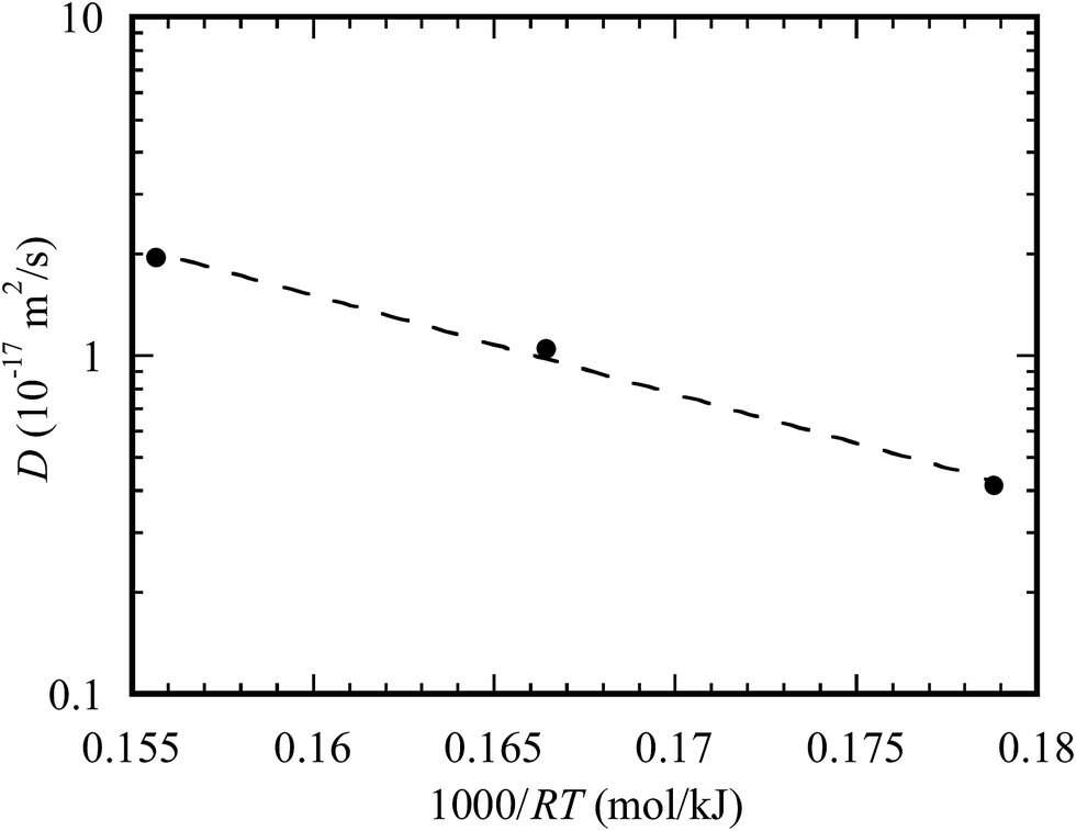 | ||
| Fig. 8 Temperature dependence of the diffusion coefficient for the diffusion of Au atoms on the outer surface of the TiO2 nanotubes. | ||
There are reports on the diffusion of Au, including self-diffusion, surface diffusion, and grain boundary diffusion. Table 2 lists the diffusivity and activation energy for the diffusion of Au reported in literature as well as the results obtained from this work. It is evident that the diffusivity of Au on the outer surface of the TiO2 nanotubes is about the same as the self-diffusivity of Au reported by Rupp et al.,41 while the activation energy is less than those for lattice diffusion and grain boundary diffusion. Such differences reveal the effect of microstructure on the diffusion behavior of Au. It is interesting to note that the activation energy for the diffusion of Au atoms on the outer surface of the TiO2 nanotubes is larger than that for the surface diffusion of Au reported by Gobel and Vonblanckenhagen45 and less than that for the grain boundary diffusion of Au reported by Ruffino.42 Such a result suggests that the migration/diffusion of Au into the TiO2 nanotube arrays involves the grain boundary diffusion and surface diffusion of Au and the interface diffusion on the surface of the TiO2 nanotubes, as schematically shown in Fig. 9.
| Temperature (°C) | Diffusivity (m2 s−1) | Activation energy (kJ mol−1) | |
|---|---|---|---|
| Lattice diffusion of Au (ref. 41) | 450 | 2.2 × 10⁻¹⁸ | 167 |
| Grain boundary diffusion of Au (ref. 42) | 27 | 2.21 × 10⁻²⁵ | 111 |
| Surface diffusion of Au (ref. 43) | 930 | 1.2 × 10⁻⁹ | 272 |
| Surface diffusion of Au (ref. 44) | 500 | 4.61 × 10⁻¹⁵ | 146.5–175 |
| Surface diffusion of Au (ref. 44) | 170 | 2.3 × 10⁻¹⁹ | |
| Surface diffusion of Au (ref. 45) | 300 | 1.9 × 10⁻¹⁵ | 38.6 |
| Surface diffusion of Au (ref. 45) | 500 | 1.2 × 10⁻¹⁴ | 38.6 |
| Au on surface of TiO2 nanotubes (this work) | 400–500 | 4.14–19.4 × 10⁻¹⁸ | 67.2 |
 | ||
| Fig. 9 Schematic of the Au diffusion on the surface of a TiO2 nanotube. | ||
In general, one can determine the average size of particles from the size distribution. From Fig. S4,† the temporal evolution of the size of Au nanocrystals near the diffusion front for the heat treatment at 500 °C is depicted in Fig. 10. It is known that the growth behavior of particles can be expressed as42
| rn − r0n = kt | (6) |
 | ||
| Fig. 10 Temporal evolution of the average size of Au nanocrystals. | ||
5. Conclusion
This work presents an approach to form Au@TiO2 nanotube arrays via the coating of Au nanofilm on the top of pure TiO2 nanotube arrays and the heat treatment in the temperature of 400 to 500 °C. The TiO2 nanotube arrays were prepared by a two-step anodization process, and the coating of Au nanofilm was prepared by magnetron sputtering. The heat treatment led to the diffusion of Au atoms in the Au nanofilm into the TiO2 nanotube arrays, resulting in the formation of Au nanocrystals on the surface of the TiO2 nanotubes. The average migration/diffusion length of Au atoms on the outer surface of the TiO2 nanotubes along the longitudinal direction of the TiO2 nanotubes increases with the increase of the heat-treatment temperature and the heating time. The size of the Au nanocrystals decreases with the increase of the distance to the top of the TiO2 nanotubes.The diffusion of Au atoms on the outer surface of the TiO2 nanotubes was analyzed by using the theory of diffusion. The diffusivity for the diffusion of Au atoms on the outer surface of the TiO2 nanotubes is in the range of 4.14–19.4 × 10⁻¹⁸ m2 s−1 for the temperature in the range of 400–500 °C. The activation energy for the migration/diffusion of Au atoms on the outer surface of the TiO2 nanotubes in the temperature range of 400 to 500 °C is 67.2 kJ mol−1, which is larger than that for the surface diffusion of Au reported by Gobel and Vonblanckenhagen45 and less than that for the grain boundary diffusion of Au reported by Ruffino.42 Such a result suggests that the diffusion of Au into the TiO2 nanotube arrays involves the grain boundary diffusion and surface diffusion of Au and the interface diffusion on the surface of the TiO2 nanotubes. The growth of Au nanocrystals on the surface of the TiO2 nanotubes can be described as the first order reaction.
Acknowledgements
LW is grateful for the financial support from the National Natural Science Foundation of China (51301118, 51274149) and the Scientific and Technological Innovation Programs of Higher Education Institutions in Shanxi province (2013108). WGZ is grateful for the support from China Scholarship Council (CSC) and the Fundamental Research Funds for the Central Universities. FY is grateful for the support from the “Hundred-People-Plan” Program of Shanxi (2014). YML is grateful for the support from Natural Science Foundation of Shanxi province (2015021066).References
- W. G. Zhang, Y. M. Liu, D. Y. Zhou, J. Wen, W. Liang and F. Q. Yang, RSC Adv., 2015, 5, 57155–57163 RSC.
- B. Kraeutler and A. J. Bard, J. Am. Chem. Soc., 1977, 99, 7729–7731 CrossRef CAS.
- Y. Nakato, A. Tsumura and H. Tsubomura, J. Phys. Chem., 1983, 87, 2402–2405 CrossRef CAS.
- Y. Nakato, H. Akanuma, J. Shimizu and Y. Magari, J. Electroanal. Chem., 1995, 396, 35–39 CrossRef.
- R. Bauer, G. Waldner, H. Fallmann, S. Hager, M. Klare, T. Krutzler, S. Malato and P. Maletzky, Catal. Today, 1999, 53, 131–144 CrossRef CAS.
- D. G. Ma, Y. Yan, H. W. Ji, C. C. Chen and J. C. Zhao, Chem. Commun., 2015, 51, 17451–17454 RSC.
- F. Xiao, Chem. Commun., 2012, 48, 6538–6540 RSC.
- L. Li, P. Zhang, W. M. Wang, H. T. Lin, A. B. Zerdoum, S. J. Geiger, Y. C. Liu, N. Xiao, Y. Zou, O. Ogbuu, Q. Y. Du, X. Q. Jia, J. J. Li and J. J. Hu, Sci. Rep., 2015, 5, 13832 CrossRef PubMed.
- J. T. Choy, J. D. B. Bradley, P. B. Deotare, I. B. Burgess, C. C. Evans, E. Mazur and M. Loncar, Opt. Lett., 2012, 37, 539–541 CrossRef CAS PubMed.
- S. Giudicatti, S. M. Marz, S. Bottner, B. Eichler, M. R. Jorgensen and O. G. Schmidt, Proc. SPIE, 2014, 9127, 912706 CrossRef.
- M. S. Kim, T. W. Lee and J. H. Parka, J. Electrochem. Soc., 2009, 156, A584–A588 CrossRef CAS.
- D. Deng, M. G. Kim, J. Y. Lee and J. Cho, Energy Environ. Sci., 2009, 2, 818–837 CAS.
- P. F. Zeng, Z. Y. Liu, Z. Y. Hu, J. Zhai and L. Jiang, RSC Adv., 2013, 3, 22853–22856 RSC.
- B. T. Zhao, S. M. Jiang, C. Su, R. Cai, R. Ran, M. O. Tade and Z. P. Shao, J. Mater. Chem. A, 2013, 1, 12310–12320 CAS.
- Z. Y. Weng, H. Guo, X. M. Liu, S. L. Wu, K. W. K. Yeung and P. K. Chu, RSC Adv., 2013, 3, 24758–24775 RSC.
- K. Hemalatha, A. S. Prakash, K. Guruprakash and M. Jayakumar, J. Mater. Chem. A, 2014, 2, 1757–1766 CAS.
- E. J. Lee, I. Nam, J. Yi and J. H. Bang, J. Mater. Chem. A, 2015, 3, 3500–3510 CAS.
- Q. L. Wu, J. C. Li, R. D. Deshpande, N. Subramanian, S. E. Rankin, F. Q. Yang and Y. T. Cheng, J. Phys. Chem. C, 2012, 116, 18669–18677 CAS.
- J. Yoo, K. Lee and P. Schmuki, Electrochem. Commun., 2013, 34, 351–355 CrossRef CAS.
- L. Huang, F. Peng, H. J. Wang, H. Yu, W. Geng, J. Yang, S. Q. Zhang and H. J. Zhao, Mater. Chem. Phys., 2011, 130, 316–322 CrossRef CAS.
- Y. H. Zhang, Y. N. Yang, P. Xiao, X. N. Zhang, L. Lu and L. Li, Mater. Lett., 2009, 63, 2429–2431 CrossRef CAS.
- Y. M. Xin, Z. Z. Li and Z. H. Zhang, Chem. Commun., 2015, 51, 15498–15501 RSC.
- G. M. Guo, B. B. Yu, P. Yu and X. Chen, Talanta, 2009, 79, 570–575 CrossRef CAS PubMed.
- Y. Y. Song, Z. D. Gao and P. Schmuki, Electrochem. Commun., 2011, 13, 290–293 CrossRef CAS.
- J. Y. Yan, H. H. Song, S. B. Yang, J. D. Yan and X. H. Chen, Electrochim. Acta, 2008, 53, 6351–6355 CrossRef CAS.
- H. Yoo, C. Bae, Y. Yang, S. Lee, M. Kim, H. Kim, Y. Kim and H. Shin, Nano Lett., 2014, 14, 4413–4417 CrossRef CAS PubMed.
- S. A. Amin, M. Pazouki and A. Hosseinnia, Powder Technol., 2009, 196, 241–245 CrossRef CAS.
- F. X. Xiao, RSC Adv., 2012, 2, 12699–12701 RSC.
- Y. H. Lu, W. G. Wang, Y. Y. Weng and W. Dong, Chin. Phys. Lett., 2015, 32, 108101 CrossRef.
- Z. Zhang, L. Zhang, M. N. Hedhili, H. Zhang and P. Wang, Nano Lett., 2013, 13, 14–20 CrossRef CAS PubMed.
- K. Shankar, G. K. Mor, H. E. Prakasam, O. K. Varghese and C. A. Grimes, Langmuir, 2007, 12445–12449 CrossRef CAS PubMed.
- A. A. Ismail, D. W. Bahnemann, I. Bannat and M. Wark, J. Phys. Chem. C, 2009, 113, 7429–7435 CAS.
- F. Xiao, J. Mater. Chem., 2012, 22, 7819–7830 RSC.
- F.-X. Xiao, Z. Zeng and B. Liu, J. Am. Chem. Soc., 2015, 137, 10735–10744 CrossRef CAS PubMed.
- F.-X. Xiao, Z. Zeng, S.-H. Hsu, S.-F. Hung, H. M. Chen and B. Liu, ACS Appl. Mater. Interfaces, 2015, 7, 28105–28109 Search PubMed.
- A. Roguska, A. Kudelski, M. Pisarek, M. Opara and M. Janik-Czachor, Appl. Surf. Sci., 2011, 257, 8182–8189 CrossRef CAS.
- D. V. Ragone, Thermodynamics of materials, Wiley, 1995 Search PubMed.
- Q. Jiang, S. Zhang and M. Zhao, Mater. Chem. Phys., 2003, 82, 225–227 CrossRef CAS.
- T. Nason, G. R. Yang, K. H. Park and T. M. Lu, J. Appl. Phys., 1991, 70, 1392–1396 CrossRef CAS.
- S. K. Ghandhi, VLSI Fabrication Principles, John wiley & sons, New York, 1983 Search PubMed.
- W. Rupp, U. Ermert and R. Sizmann, Phys. Status Solidi, 1969, 33, 509–516 CrossRef CAS.
- F. Ruffino, M. G. Grimaldi, C. Bongiorno, F. Giannazzo, F. Roccaforte, V. Raineri and C. Spinella, J. Appl. Phys., 2009, 105, 054311 CrossRef.
- M. Mclean and J. P. Hirth, Surf. Sci., 1968, 12, 177–188 CrossRef CAS.
- T. S. Lin and Y. W. Chung, Superlattices Microstruct., 1988, 4, 709–712 CrossRef CAS.
- H. Gobel and P. Vonblanckenhagen, Surf. Sci., 1995, 331, 885–890 CrossRef.
Footnote |
| † Electronic supplementary information (ESI) available. See DOI: 10.1039/c6ra08801e |
| This journal is © The Royal Society of Chemistry 2016 |