
Surface flattening of a polyimide layer in a liquid crystal cell fabricated by using a field-induced UV-alignment method
Seung-Won Oh ,
Jong-Min Baek,
Jun-Hee Park and
Tae-Hoon Yoon*
,
Jong-Min Baek,
Jun-Hee Park and
Tae-Hoon Yoon*
Department of Electronics Engineering, Pusan National University, Busan 46241, Korea. E-mail: thyoon@pusan.ac.kr; Fax: +82-51-515-5190; Tel: +82-51-510-2379
First published on 3rd June 2016
Abstract
We previously published a liquid crystal alignment method using an ultraviolet (UV)-curable polymer for the near-zero pretilt angle. We have shown that the pretilt angle can be lowered by curing a reactive mesogen in the alignment layer while applying a vertical electric field. In this study, we analyzed the mechanism behind these observations. Using X-ray photoelectron spectroscopy, we confirmed that the C 1s and O 1s peaks show neither a wavelength shift nor an intensity change by UV curing, regardless of application of an electric field. We also confirmed the characteristics of the flattened surface after UV curing under an applied electric field, using atomic force microscopy. We found by atomic force microscopy that the decrease in pretilt angle is related to the flattened surface in a homogeneously aligned LC cell fabricated with the field-induced UV-alignment method.
Introduction
Various methods are used for liquid crystal (LC) alignment, including the rubbing of polymer films,1 evaporation of silicon monoxide, and plasma and ion-beam irradiation.2–6 Mechanical rubbing has been widely used to provide uniaxial LC alignment. However, the rubbing method has several problems, including electrostatic charging, production of debris, and mechanical stress, which generate local defects and streaks, thereby resulting in display resolution degradation. Photoalignment technology has recently been the focus of many research efforts to achieve high display performance in homogeneously aligned LC devices.7–10 Even though photoalignment has various advantages and can overcome the drawbacks of the rubbing process, it has not yet been widely applied in mass production because of its weak surface anchoring energy, process complexity, high curing energy, and severe image sticking.Our group recently proposed a field-induced ultraviolet (UV)-alignment method to achieve a near-zero pretilt angle in a homogeneously aligned LC cell.11,12 We demonstrated that with this method the pretilt angle can be decreased from 2.390° to 0.082° and a symmetric luminance distribution in the dark state can be obtained. However, the underlying mechanism has not yet been investigated.
In this paper, we present our investigation of the pretilt angle lowering effect achieved using the field-induced UV-alignment method, and analyze its underlying mechanism. As will be discussed, we found that the decrease in pretilt angle is be related to the flattened surface in a homogeneously aligned LC cell fabricated with the field-induced UV-alignment method. After UV curing under an applied electric field, we can confirm the flattened microgrooves.
Experimental
To fabricate an LC cell using the field-induced UV-alignment method, indium-tin-oxide (ITO) coated glass substrates were subjected to several cleaning steps before the rubbing process. A mixture of the planar alignment material (PIA-5310-GS10: JNC, Japan), reactive mesogen (RM 257: Merck, Germany), and photoinitiator (Irgacure 651: BASF, Germany) was spin-coated on each substrate. The chemical structures of these monomers are shown in Fig. 1(a). The mixture was spin-coated at 3000 rpm, for 30 s. The coated substrates were pre-baked at 100 °C for 10 min on a hot plate and annealed at 180 °C for 1 h. Each substrate was rubbed with cotton after the baking process. The average values of the fiber diameter, the fiber length, and the fiber density were 15 μm, 2.5 mm, and 1040 cm−2, respectively. The diameter of the rubbing roller, the rubbing depth (or the pile pressed depth), the rotation speed of the roller, and the substrate proceeding speed were 60 mm, 0.25 mm, 1000 rpm, and 33 mm s−1, respectively.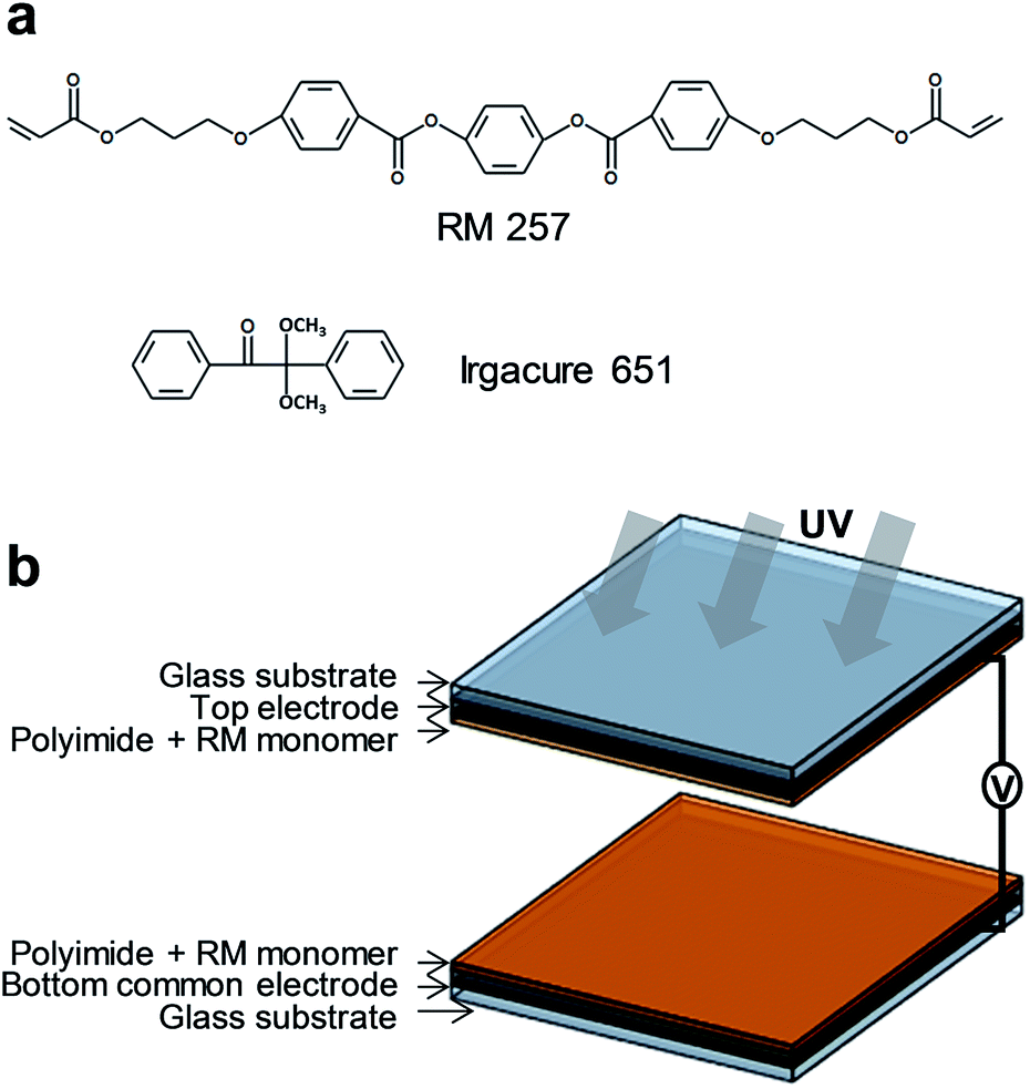 | ||
| Fig. 1 (a) Chemical structures of the photoreactive monomer and photoinitiator. (b) Device structure for the field-induced UV-alignment method. | ||
Having completed these processes, the cells were assembled using silica spacers with a diameter of 5 μm. Negative LC (MLC-6608: Δn = 0.083, Δε = −4.2, Merck) was injected into each cell by capillary action at room temperature. The LC cells were then exposed to unpolarized UV light (365 nm) with an intensity of 10 mW cm−2 using a mercury arc lamp (Osram HBO 103 W/2), under an applied vertical electric field of 20 V, as shown in Fig. 1(b). A UV curing time was 30 min. As a result, a near-zero pretilt angle was obtained in homogeneously aligned negative LC cells.
Results and discussion
We first investigated the pretilt angle of the LC molecules as a function of the reactive mesogen (RM) concentration. The pretilt angle was measured using, at least, three samples by the crystal rotation method.13 As shown in Fig. 2, although the pretilt angles of the samples obtained without application of an electric field were higher than 1°, the pretilt angle decreased as the RM concentration increased. This reduction in the pretilt angle is caused by the azimuthal anchoring energy enhanced by the RM in the alignment layer.11,14 The pretilt angles of the samples obtained with application of an electric field were 0.149° (RM 0.5 wt%) and 0.130° (RM 1.0 wt%), which are much lower than the pretilt angles of 1.73° (RM 0.5 wt%) and 1.39° (RM 1.0 wt%) obtained without application of an electric field.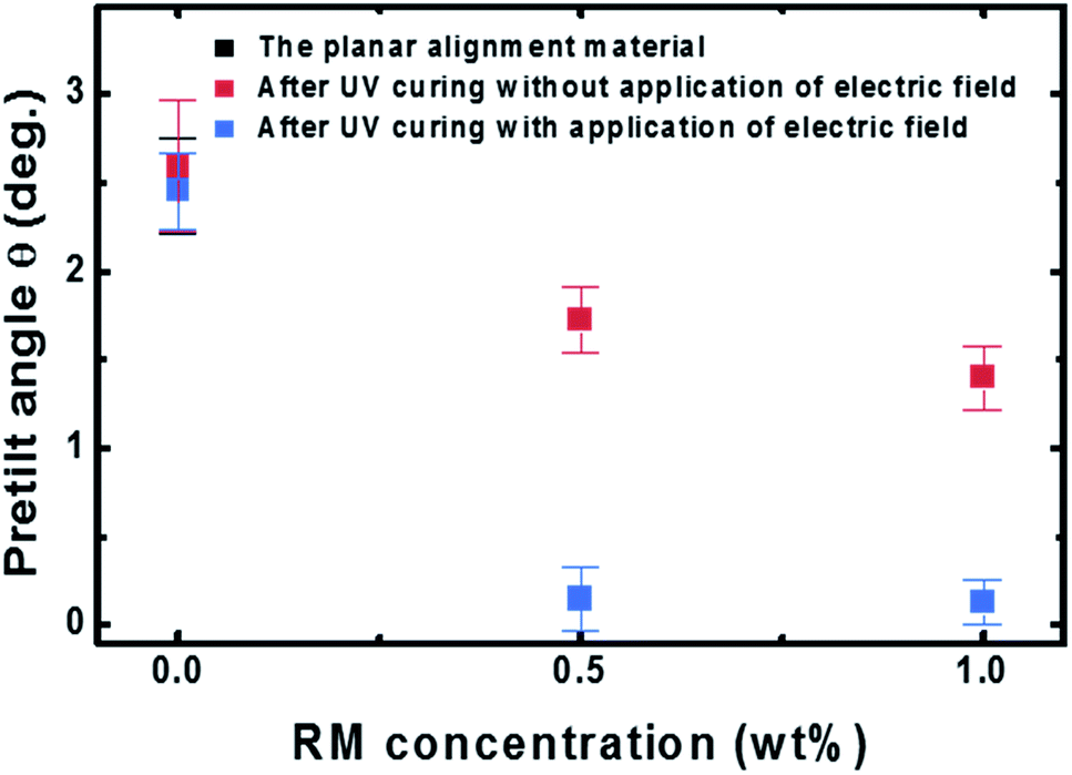 | ||
| Fig. 2 Measured pretilt angle vs. the RM concentration. | ||
To understand the decrease of the pretilt angle, we calculated the effect of the applied electric field on the tilt angle. We can estimate the surface pretilt to be built on top of the polymerized layer at a specific applied voltage and a layer thickness.15,16 For example, when a monomer layer with thickness of 200 nm is polymerized under an applied fields of 20 V and 50 V, the estimated pretilt angles are approximately 0.768° and 0.126°, respectively. However, the measured pretilt angle of 0.130° at an applied voltage of 20 V were lower than the estimated value of 0.768°. These results cannot be explained only by the formation of the polymer structure on a substrate surface.16
Surface energy is one of the important factors to control the pretilt angle on the alignment surface. Fig. 3 shows the measured contact angle as a function of the RM concentration. The distilled water contact angle of substrates was measured at room temperature using a contact angle measurement system (Easy Drop, KRUSS, Germany). The contact angle after UV curing decreased as the RM concentration was increased because of their hydrophobic properties.17 Similarly, the pretilt angle after UV curing decreased as the RM concentration increased, as shown in Fig. 2. The decrease in both contact angle and pretilt angle was caused by the increase in surface energy.17 The contact angles of the samples obtained with application of an electric field were lower than those obtained without application of an electric field, even though the same amount of RM was used. However, the differences were small and the difference in surface energy is not a cause of the difference in pretilt angle in our method. We analyzed the surface chemistry using X-ray photoelectron spectroscopy (XPS) and the surface roughness using atomic-force microscopy (AFM).
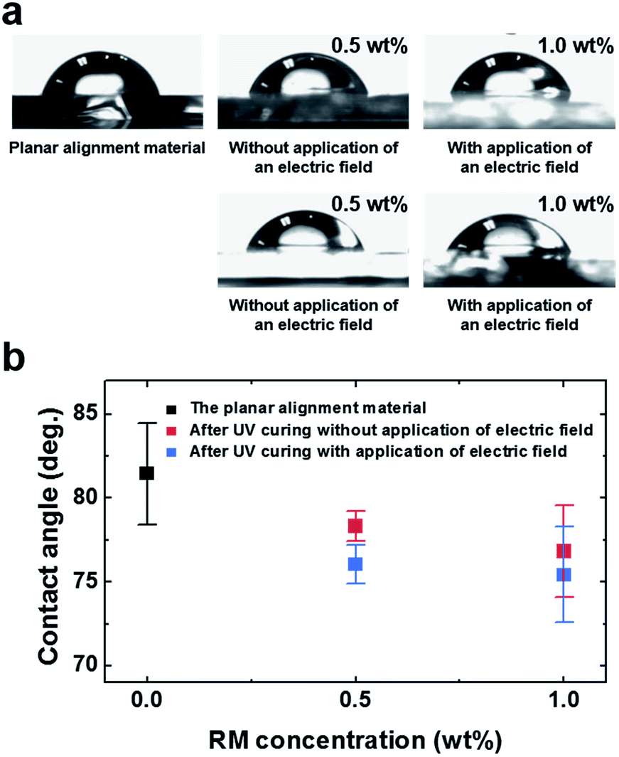 | ||
| Fig. 3 (a) Photographs of the contact angles. (b) Contact angles vs. the RM concentration. | ||
An X-ray photoelectron spectroscope was used to analyze the chemical composition of the substrate (Theta Probe AR-XPS System, Thermo Fisher Scientific, U.K.), with a monochromatic Al X-ray source (Al-Kα line: 1486.6 eV) and a 15 kV, 150 W power source. The XPS spectra were processed with a fitting routine, which can decompose each spectrum into individual sub-spectra, for information on specific bondings. To determine the effect of RM on the pretilt angle of the LC, we analyzed the XPS spectra after UV curing with or without application of an electric field.
Fig. 4(a) shows the changes in the core-level XPS spectra of the C 1s peaks. The low-binding-energy component peak centered at 284.6 eV is due to the C–C bond, whereas the peak at 286.2 eV is related to the C–O bond; another component peak at 288.5 eV corresponds to the O![[double bond, length as m-dash]](https://www.rsc.org/images/entities/char_e001.gif) C double bond.18,19 The XPS spectra for the O 1s peaks were also obtained, and are shown in Fig. 4(b). The component peak centered at 531.6 eV corresponds to the OC double bond, whereas the peak at 533.0 eV is due to the O–C single bond. We should note that the C 1s and O 1s peaks showed no peak shift or significant difference in intensity after UV curing, regardless of application of an electric field.
C double bond.18,19 The XPS spectra for the O 1s peaks were also obtained, and are shown in Fig. 4(b). The component peak centered at 531.6 eV corresponds to the OC double bond, whereas the peak at 533.0 eV is due to the O–C single bond. We should note that the C 1s and O 1s peaks showed no peak shift or significant difference in intensity after UV curing, regardless of application of an electric field.
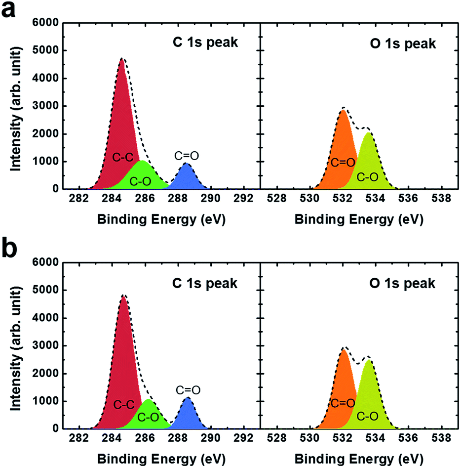 | ||
| Fig. 4 XPS spectra of C 1s and O 1s peaks, confirming the photopolymerization of the RM after UV curing (a) without and (b) with application of an electric field. | ||
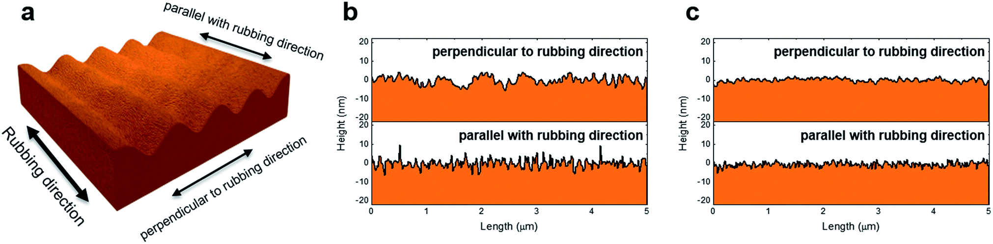 | ||
| Fig. 5 (a) AFM tip scanning directions. Line profiles generated by AFM analysis after UV curing (b) without and (c) with application of an electric field. | ||
The substrate surface was studied using AFM analysis. For AFM measurements, substrates were separated and washed with isopropyl alcohol and distilled water for a couple of minutes. The morphology evaluation was carried out using an atomic force microscope (Nanosurf EasyScan 2 AFM system, Nanosurf AG, Switzerland). RMS surface roughness were determined by using AFM images (5 × 5 μm2). To determine the errors of AFM analysis, we compared three samples which were fabricated at the same condition. The surface profile of samples after UV curing without application of an electric field showed periodic microgrooves, which were generated by rubbing. After UV curing with application of an electric field, the root-mean-square (RMS) roughness decreased slightly, from 0.497 nm to 0.232 nm for the direction perpendicular to the rubbing direction and from 0.536 nm to 0.335 nm for the direction parallel with the rubbing direction, as shown in Fig. 5, respectively. Interestingly, the monomers prefer to fill the microgrooves while the polymer network is being formed on the substrate surface. The profile, therefore, showed a non-periodic surface topology and the RMS roughness decreased.
The microgrooves were filled and the tilt angle of the polyimide molecules decreased. Although the pretilt angle of the LC decreased mainly by the formation of polymer structure on a substrate surface, the flattened surface may also have led to a decrease in the pretilt angle of the LC. We should note that UV curing with application of an electric field can be used to modify the surface topography and lower the LC pretilt angle.
Conclusions
We analyzed the mechanism underlying the pretilt angle lowering effect achieved by the field-induced UV-alignment method. Although a sufficiently high electric field was not applied to the cells, the measured pretilt angle of samples was lower than the estimated value. We have investigated this difference through the change in surface roughness and chemistry. The XPS results showed neither peak shifts nor intensity change by UV curing, regardless of application of an electric field. In contrast, the surface roughness did change with application of an electric field, even though the surface chemistry did not. We confirmed the surface flattening effect of UV curing with application of an electric field by AFM analysis. The AFM results show that the decrease in pretilt angle is related to the flattened surface in a homogeneously aligned LC cell fabricated with the field-induced UV-alignment method. We expect that the developed technology can be used for display applications as one of the LC alignment techniques by which we can eliminate the off-axis light leakage by lowering of the pretilt angle.Acknowledgements
This work was supported by the National Research Foundation of Korea (NRF) grant funded by the Korea government (MSIP) (No. 2014R1A2A1A01004943).Notes and references
- P. Chatelain, C. R. Hebd. Seances Acad. Sci., 1936, 203, 1169 CAS.
- J. L. Janning, Appl. Phys. Lett., 1972, 21, 173 CrossRef CAS.
- M. Schadt, K. Schmitt, V. Kozinkov and V. Chigrinov, Jpn. J. Appl. Phys., 1992, 31, 2155 CrossRef CAS.
- P. Chaudhari, J. Lacey, J. Doyle, E. Galligan, S.-C. A. Lien, A. Callegari, G. Hougham, N. D. Lang, P. S. Andry, R. John, K.-H. Yang, M. Lu, C. Cai, J. Speidell, S. Purushothaman, J. Ritsko, M. Samant, J. Stöhr, Y. Nakagawa, Y. Katoh, Y. Saitoh, K. Sakai, H. Satoh, S. Odahara, H. Nakano, J. Nakagaki and Y. Shiota, Nature, 2001, 411, 56 CrossRef CAS PubMed.
- O. Yaroshchuk, Y. Zakrevskyy, A. Dobrovolskyy and S. Pavlov, Proc. SPIE, 2001, 4418, 49 CrossRef CAS.
- P. K. Son, J. H. Park, S. S. Cha, J. C. Kim, T.-H. Yoon, S. J. Rho, B. K. Jeon, J. S. Kim, S. K. Lim and K. H. Kim, Appl. Phys. Lett., 2006, 88, 263512 CrossRef.
- T.-J. Chen and K.-L. Chu, Appl. Phys. Lett., 2008, 92(9), 091102 CrossRef.
- J. W. Woo, D. C. Shin, E. J. Lim, H. J. Park and H. H. Shin, Proc IDW ’08, 2008, 37.
- O. Yaroschchuk, V. Kyrychenko, D. Tao, V. Chigrinov, H. S. Kwok, H. Hasebe and H. Takatsu, Appl. Phys. Lett., 2009, 92, 021902 CrossRef.
- H. J. Ahn, C. S. Lim, D. J. Kim, J. H. Lee, H. J Park, S. B. Lee, J. W. Woo, W. S. Shin and M. C. Jun, Dig. Tech. Pap.–Soc. Inf. Disp. Int. Symp., 2012, 43, 1432 CrossRef.
- S.-W. Oh, J.-H. Park and T.-H. Yoon, Opt. Express, 2015, 23, 1044 CrossRef PubMed.
- S.-W. Oh, J.-H. Park and T.-H. Yoon, J. Disp. Technol., 2016, 12, 40 CrossRef.
- M.-P. Cuminal and M. Brunet, Liq. Cryst., 1997, 22, 185 CrossRef CAS.
- Y. Kim, Y.-J. Lee, D.-H. Kim, J.-H. Baek, J.-H. Lee, B.-K. Kim, C.-J. Yu and J.-H. Kim, J. Phys. D: Appl. Phys., 2013, 46, 485306 CrossRef.
- S.-T. Wu and D.-K. Yang, Fundamentals of Liquid Crystals Devices, Wiley, 2006 Search PubMed.
- L. Lu, T. Sergan, V. Serga and P. J. Bos, Appl. Phys. Lett., 2012, 101, 251912 CrossRef.
- K. Takatoh, M. Hasegawa, M. Koden, N. Itoh, R. Hasegawa and M. Sakamoto, Alignment Technologies and Applications of Liquid Crystal Devices, Taylor & Francis group, LLC, 2005 Search PubMed.
- A. Hamwi, C. Latouche, V. Marchand, J. Dupuis and R. Benoit, J. Phys. Chem. Solids, 1996, 57, 991 CrossRef CAS.
- S. Delpeux, F. Beguin, R. Benoit, R. Erre, N. Manolova and I. Rashkov, Eur. Polym. J., 1998, 34, 905 CrossRef CAS.
| This journal is © The Royal Society of Chemistry 2016 |