DOI:
10.1039/C6RA07564A
(Paper)
RSC Adv., 2016,
6, 53794-53799
Multiconfigurable logic gate operation in 1D polydiacetylene microtube waveguide†
Received
23rd March 2016
, Accepted 19th May 2016
First published on 19th May 2016
Abstract
Recently, multiconfigurable logic gate operation in one-dimensional (1D) nano/micrometer-sized waveguide materials have attracted enormous attention due to their potential applications in ultrafast information processing and optical computing systems, since 1D nano/micrometer-sized waveguides can directly act as the key building blocks of miniaturized optoelectronics. Herein, we designed and fabricated viologen-functionalized polydiacetylene (VFPDA) microtubes via a thiol–ene based ‘click’ reaction, and the tip emission of the VFPDA microtube exhibited a strong dependence on thermal or electrical stimuli, and the polarization of the excited linearly polarized light. Various basic logic gates (NOR, AND, INH) and combinational logic circuits (INH–INH, AND–INH) were constructed successfully by using two or three of the above triggers as the input signals, and the tip emission of a VFPDA microtube as the output signal. We expected this novel resettable multiconfigurable logic gate operation in micrometer-sized waveguides to show promising new opportunities in miniaturized electro-optical switches, smart integrated optical devices and circuits for future information technology.
Introduction
One-dimensional (1D) nano/micrometer-sized polymer waveguides have attracted enormous attention due to their unique properties including excellent processing properties, chemically tunable optoelectronic characteristics, and their potential applications in optical communications, sensing and integrated optoelectronic devices.1–3 Liu et al. reported 1D dye doped polymer or quantum dot/polymer composite nanofibers by an electro-spinning method.4 Redmond et al.5 and Fasano et al.6 fabricated 1D polyfluorene based nanofiber waveguides and optically pumped lasing behavior. However, the transport light in above 1D nano/micrometer-sized polymer waveguides is predetermined and cannot be modulated reversibly, limiting their practical applications in smart optoelectronics. In our previous work, 1D polydiacetylene (PDA)7 and spiropyran-functionalized PDA (SFPDA) microtube8 had been prepared, and modulation of waveguiding in above PDA based microtube waveguide had been achieved upon external pH, thermal or light stimuli. And various resettable, basic logic operations (including OR and INHIBIT) in SFPDA microtube have been achieved by using light and pH stimuli as the as the input signals, and the tip emission of the microtube as the output signal. However, the challenge of performing multiconfigurable logic operation in above nano/micrometer-sized polymer waveguides by using multiple input signals, which promise new opportunities in integrated smart optoelectronic devices and optical computing systems for future information technology, has not been described to date. Compared to other external stimuli, electrical stimuli have received increasing attentions they can be applied remotely, rapidly, locally, reversibly and maintaining the mild conditions of system.9 Therefore the combination of the electronic and photonic component in one miniaturized functional devices to provide complicated logic computing, memory and interconnect functions has proved challenging, owing to their promising applications in information microprocessor, photonic circuit elements, electro-optic transmitters and so on.10–14 Up to now, only a few studies have dealt with the fabrication of electrical modulation of waveguiding in 1D nano/microstructures.15,16 However, most of above built systems usually lack good reversibility and stability, as well as high on/off contrast and low operation voltage, limiting their practical applications. Further, basic or multiconfigurable logic operation in 1D nano/micrometer-sized materials by receiving electrical signal as the input signal have not been realized. In this regard, development of novel electrical-response 1D nano/micrometer-sized waveguide and further achieving multiconfigurable logic operation using electrical stimuli as one of the input signal still remain a big challenging.
Herein, we designed and synthesized viologen-functionalized PDA (VFPDA) microtubes via thiol–ene based ‘click’ reaction. The modulation of waveguiding in VFPDA microtubes could be realized based on FRET between PDA matrix and the electrical-responsive viologen units at the interface. Moreover, the waveguide performance and tip emission intensity of PDA microtube matrix were found to be dependent on the external thermal or electrical stimuli, and the polarization direction of the excited linearly polarized light. It is anticipated that multiconfigurable logic operation in above VFPDA microtube waveguide could be achieved by using thermal, linearly polarized light and electrical triggers as the input signal and the tip emission of VFPDA microtube waveguide as the output signal. We expected this novel materials to have a variety of applications in ultrafast information processing, photonic circuits, and optical computing.
Experimental section
Materials
10,12-Pentacosadiynoic acid (PCDA), purchased from Tokyo Chemical Industry Co., Ltd., was used as received. 4,4′-Bipyridyl, 3-bromopropene, allylglycidyl ether, 1,2-ethanedithiol, Irgacure 2959, were purchased from Aldrich and used as received. N,N′-Diallyl-4,4′-bipyridinium was synthesized according to the reference.17 The molecular structure and the synthesis route of N,N′-diallyl-4,4′-bipyridinium was shown in Fig. S1.† All other solvents and reagents were of analytical grade and used as received. Milli-Q water (18.2 MΩ cm) was used in all cases.
The preparation of viologen-functionalized PDA (VFPDA) microtubes
Amine-functionalized PDA microtube were prepared by a hierarchical self-assembly procedure.7 Then allylglycidyl ether aqueous solution (200 μl, 3 mmol) was added dropwise to above PDA microtubes suspension solution, and above mixture was stirred and stored in an incubator at room temperature for 10 h to ensure the surface modification reaction complete. After rinsing with deionized water for 3 times in order to remove unreacted allyl glycidyl ether and other impurities, the vinyl-functionalized PDA microtube were prepared successfully. Finally, VFPDA microtubes were prepared through the interfacial ‘click’ reaction. The click reaction were performed by irradiation with a UV-lamp (with 365 nm interface filter, Δλ = 10 nm, light intensity 20 mW cm−2) at room temperature for 30 min.
Characterization
FTIR and 1H NMR spectra experiments were carried out with a MAGNA 750 FT-IR Spectrometer and a JEOL FX-90Q NMR 400 spectrometer, respectively. Transmission electron microscopy (TEM) characterization and scanning electron microscopy (SEM) were performed on a JEOL-2000 microscope (operated at 200 kV) and a FEISirion 200 system, respectively. The Fluorescence spectra and UV-Vis absorption spectra were characterized on a JY-ihR 550 spectrophotometer and a SHIMADZU UV-2550 PC spectrophotometer, respectively. Confocal laser scanning microscopy (CLSM) images and optical microscopy images were obtained in Olympus, FV 300 andBX-51 fluorescence microscope, respectively. X-ray photoelectron spectroscopy (XPS) experiments were performed by using a VG ESCALAB MK-II photoelectron spectrometer. The Raman spectra were characterized by using a LABRAM-HR Confocal Laser Micro Raman Spectrometer (514.5 nm) radiation at room temperature.
Results and discussions
Preparation and characterization of electrical-responsive VFPDA microtubes
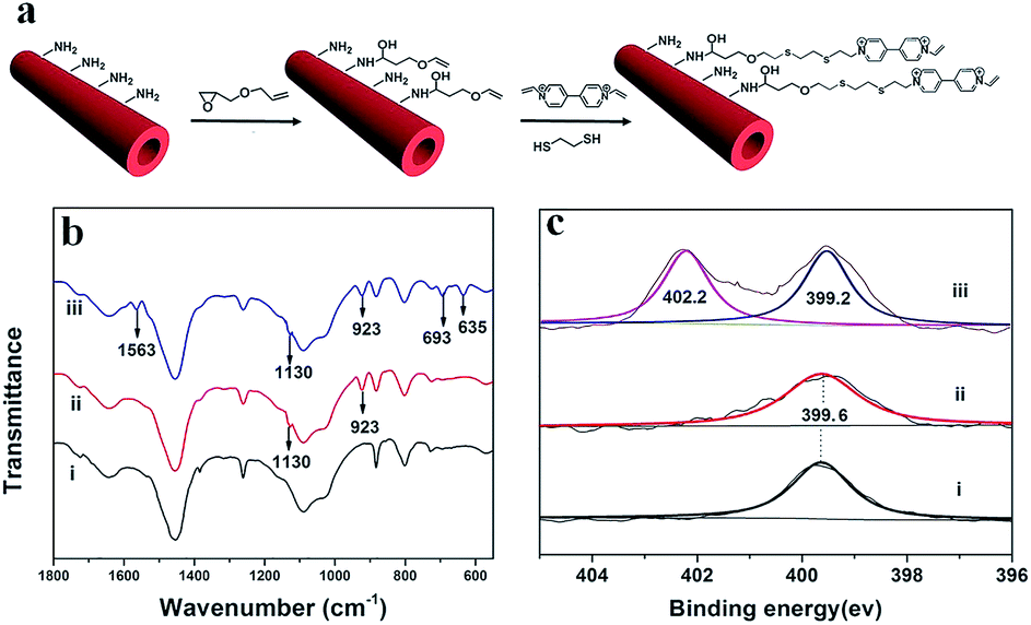
Amine-functionalized PDA microtube, about 1–3 μm in the outer diameter, were prepared by a hierarchical self-assembly procedure.7 The laser confocal microscopy characterization also confirmed the hollow microtube structure (Fig. S2†). VFPDA microtubes were synthesized via interfacial click reactions (as shown in Fig. 1a), which were monitored by FTIR and X-ray photoelectron spectroscopy (XPS) characterization. After incubation with allylglycidyl ether aqueous solution for 10 h, two new characteristic band of the stretching vibration of the C–O–C and the CH![[double bond, length as m-dash]](https://www.rsc.org/images/entities/char_e001.gif) C bond for the allyl group emerged at 1130 cm−1 and 923 cm−1, respectively (Fig. 1b, curve ii), confirming the successfully preparation of the vinyl-modified PDA microtubes. Then VFPDA microtubes were prepared through the interfacial ‘click’ reaction. After ‘click’ reaction, the characteristic bands for the pyridine ring-stretching mode and the ν(C–S) stretching modes emerged at 1563 cm−1, 693 cm−1 and 635 cm−1, respectively, confirming the successful surface modification of PDA microtubes with the viologen units. A new N 1s core level peak emerged at 402.2 eV (Fig. 1c), which should be assigned to the nitrogen elements of pyridine ring in dicationic state. All above results demonstrated that VFPDA microtubes had been successfully prepared via interfacial ‘click’ reaction.
C bond for the allyl group emerged at 1130 cm−1 and 923 cm−1, respectively (Fig. 1b, curve ii), confirming the successfully preparation of the vinyl-modified PDA microtubes. Then VFPDA microtubes were prepared through the interfacial ‘click’ reaction. After ‘click’ reaction, the characteristic bands for the pyridine ring-stretching mode and the ν(C–S) stretching modes emerged at 1563 cm−1, 693 cm−1 and 635 cm−1, respectively, confirming the successful surface modification of PDA microtubes with the viologen units. A new N 1s core level peak emerged at 402.2 eV (Fig. 1c), which should be assigned to the nitrogen elements of pyridine ring in dicationic state. All above results demonstrated that VFPDA microtubes had been successfully prepared via interfacial ‘click’ reaction.
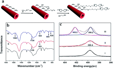 |
| | Fig. 1 (a) Preparation of VFPDA microtubes. (b) FT-IR characterization and (c) X-ray photoelectron spectra of N 1s for (i) pure PDA microtubes (ii) vinyl-modified PDA microtube, and (iii) VFPDA microtubes, respectively. | |
Modulation of waveguiding in VFPDA microtubes
A 532 nm excitation light were launched onto the body of VFPDA microtube and their optical waveguiding performance was studied by single-tube photoluminescence (PL) imaging technique.
The “blue phase” VFPDA microtube was non-fluorescent, and no out-coupled light at the tip could be observed. Upon exposure to HCl or heating treatment, a strong blue-to-red color transition was observed for the VFPDA microtube and exhibited strong red emission at 640 nm and 570 nm. A bright spot of PL at tips of the microtube could be observed under the radiation of a focused 532 nm laser, however, the body of VFPDA microtube exhibited comparatively weaker emission. Light was transported within the microtube through the intrinsic fluorescence of “red-phase” PDA, confirming VFPDA microtube as an active waveguide. The tip emission of VFPDA microtube could be easily controlled and modulated by external thermal stimuli (Fig. S3†), suggesting their potential application in sensor and smart photonic devices. By increasing the propagation length, the out-coupled tip emission of VFPDA microtube decreased almost exponentially. The loss coefficient α of single VFPDA microtube was calculated to be 425 cm−1 (±10%, the propagation loss was about 0.21 dB μm−1) (Fig. S4†), similar with the value (405 cm−1) of pure PDA microtube (the propagation loss was about 0.18 dB μm−1).7 All above results indicated that the modification of the viologen units within the surface of VFPDA microtube almost have no influence on its waveguide performance.
When applying the voltage of −1.5 V, the colorless viologens units in MV2+ state transferred to blue MV+ state (Fig. S5†), and the fluorescence of PDA microtube matrix dramatically decreased, since the absorption band of viologens in MV+ state overlaps with the fluorescence spectra of PDA microtube matrix (based on fluorescence resonance energy transfer (FRET) mechanism, Fig. S6†). Therefore the out-coupled tip emission intensity of single VFPDA microtube dramatically decreased (Fig. 2b and c). However, when applying the voltage of 1.5 V, the viologen units transferred back to colorlessMV2+ state, and the body fluorescence intensity and the out-coupled emission at the tips of single VFPDA microtube both returned to original values (Fig. 2c), since the absorption band of viologens in colorless MV2+ did not overlap with the fluorescence spectra of PDA microtube matrix (Fig. S6†). All above results indicated that reversible modulation of waveguide performance in single VFPDA microtube could be achieved upon electrical treatment, which should be ascribed to the interfacial FRET between PDA microtube matrix and the MV+ form of viologen units within the surface of VFPDA microtube (Fig. S7†).
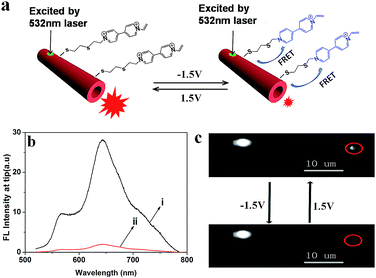 |
| | Fig. 2 (a) Electrical modulation of waveguiding in single VFPDA microtube. (b) Tip emission spectra of single VFPDA microtube with the applying voltage of (i) 1.5 V and (ii) −1.5 V. (c) FL microscope images collected upon excitation of the same VFPDA microtube following the driven voltage of 1.5 V and −1.5 V. | |
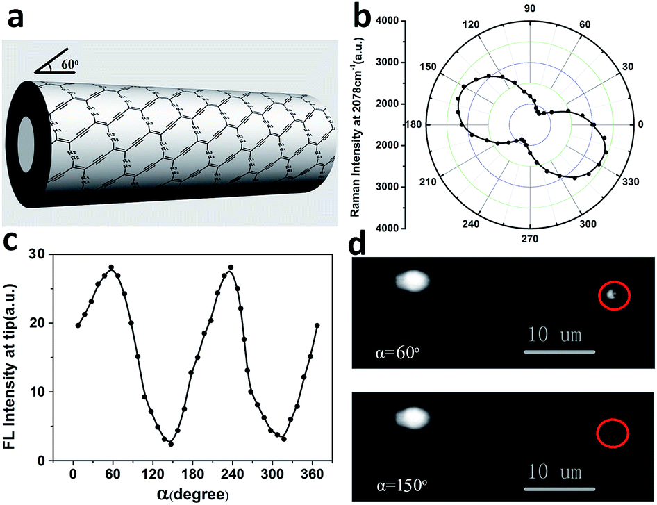
As reported previously,18 the intrinsic alignment of PDA chains within the microtube matrix could be rigorously controlled by the polarization state of linearly polarized UV light used in the polymerization procedure. Therefore, the resulting PDA microtube exhibited interesting polarization properties of fluorescence emitting and the tip emission of the microtube exhibited strong dependence on the polarization state of the excited linearly polarized 532 nm laser. As shown in Fig. 3a, the alignment of PDA chains within VFPDA microtube matrix were highly ordered and the slip angle between the orientation of PDA chains and the microtube axis is about 60°, which was confirmed by Raman characterization (Fig. 3b). As expected, the out-coupled tip emission of the microtube was found to be sensitive to the polarization state of the excitation beam (Fig. 3c). The maximum tip emission occurred when the polarization of the excitation beam was 60°, while the minimum tip emission occurred when the polarization of the excitation beam was 150°. Therefore, by varying the polarization state of the excitation beam, tip emission of VFPDA microtube could easily be controlled and modulated (Fig. 3d).
 |
| | Fig. 3 (a) Scheme of the alignment of VPDA main chain in the microtube. (b) The Raman intensity at 2078 cm−1 for the C![[triple bond, length as m-dash]](https://www.rsc.org/images/entities/char_e002.gif) C stretching vibrations as a function of the polarizer rotation angle. (c) The tip fluorescence emission intensity of VFPDA versus incident polarization rotation angle. (d) FL microscope images collected upon excitation of the same VFPDA microtube with the polarization of the excitation beam (up: 60°, down: 150°). C stretching vibrations as a function of the polarizer rotation angle. (c) The tip fluorescence emission intensity of VFPDA versus incident polarization rotation angle. (d) FL microscope images collected upon excitation of the same VFPDA microtube with the polarization of the excitation beam (up: 60°, down: 150°). | |
Basic logic operation in single VFPDA microtube
As mentioned above, the tip emission of VFPDA microtube exhibited strong dependence on the thermal, electrical stimuli, and the polarization of the excited linearly polarized light. It is anticipated that various basic logic operation in above VFPDA microtube waveguide could be achieved by using two of above triggers (thermal, electrical stimuli, and the polarization of the excited linearly polarized light) as the input signal and the tip emission of VFPDA microtube waveguide as the output signal. For example, we defined the “blue phase” VFPDA microtube (viologens units in MV+ state with applying voltage of −1.5 V) as the initial state. Upon heating treatment, “blue phase” VFPDA microtube transferred to “red phase”. However, the tip emission remained weak due to the interfacial FRET between PDA microtube matrix and the MV+ form of viologen units within the surface of the microtube. When applying the voltage of 1.5 V, the viologens units in MV+ state transferred to colorless MV2+ state (which avoided the quenching effect for PDA matrix), and the microtube exhibited strong tip emission in this case. Based on above results, an AND logic gate operation could be achieved. Herein, the heating treatment and electrical stimuli (1.5 V) as the two inputs, and the presence and absence of them were defined as “1” and “0”, respectively. For output, we defined strong tip emission as“1”, while weak tip emission as “0” with a threshold value of 5. As shown in Fig. 4, in the initial state (input 0/0), PDA microtube in the blue phase exhibited non-fluorescent and the output signal was regarded as “0”. Upon heating treatment (input 1/0), PDA microtube exhibited weak tip emission (output “0”) due to the interfacial FRET between PDA microtube matrix and viologen units in the MV+ form, although PDA microtube was in the red phase. Upon only applying the voltage of 1.5 V (input 0/1), PDA microtube remained non-fluorescent and the output signal was regarded as “0”. Upon both heating treatment and applying the voltage of 1 V (input 1/1), strong tip emission (output 1) could be detected. In this case, PDA microtube was in the red phase due to heating treatment. The viologen units in the colorless MV2+ form, and no FRET occurred between PDA microtube matrix and viologen units in MV2+ form. Therefore, strong tip emission (output 1) could be detected only in the presence of both inputs (1/1), suggesting that the system behaved as an AND logic gate. An INHBIT logic gate could be realized by a similar mechanism. We defined the “blue phase” VFPDA microtube (viologen units in MV2+ state with applying voltage of 1.5 V) as the initial state. The heating treatment and electrical stimuli (−1.5 V) as the two inputs, and the presence and absence of them were defined as “1” and “0”, respectively. The tip emission were defined as output, strong tip emission as“1”, while weak tip emission as “0”. Before treatment (input 0/0), the tip emission of the VFPDA microtube was weak since PDA microtube matrix was in blue phase and the output signal was regarded as “0”. Upon applying heating treatment alone (input 1/0), PDA microtube transferred to red phase and exhibited strong tip emission (since viologen units in the MV2+ form, no FRET occurred). And the output signal was regarded as“1”. Upon applying the voltage of 1.5 V alone (input 0/1), PDA microtube matrix remained blue phase and the output signal was regarded as“0”. Upon applying both input, PDA microtube transferred to red phase and viologen units transferred to blue MV+ form upon applying the voltage of −1.5 V. FRET occurred between PDA microtube matrix and viologen units in MV+ form within the surface of the microtube. Thus the tip emission was weak and the output signal was regarded as“0”. Strong tip emission (output 1) could be detected only upon applying heating treatment alone (input 1/0, Fig. 5), suggesting that the system behaved as an INHBIT logic gate. Furthermore, for different starting condition or input combinations, various different basic logic gate (including NOR, INH logic gate) operations could be achieved in single VFPDA microtube by similar mechanism (as shown Fig. S8 and S9†).
 |
| | Fig. 4 (a) Scheme of the design strategy for AND logic based on the VFPDA microtube. (b) Truth table for the AND gate. (c) Tip emission spectra of single VFPDA microtube of AND gate with different combinations of the inputs upon excitation at 532 nm. (d) The fluorescence intensities of tip emission for the AND logic gate. | |
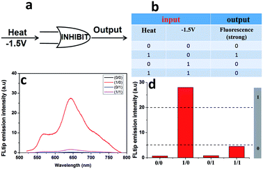 |
| | Fig. 5 (a) Scheme of the design strategy for INHIBIT logic based on the VFPDA microtube. (b) Truth table for the INHIBIT gate. (c) Tip emission spectra of single VFPDA microtube of INHIBIT gate with different combinations of the inputs upon excitation at 532 nm. (d) The fluorescence intensities of tip emission for the INHIBIT logic gate. | |
Concatenated logic gates operation in single VFPDA microtube
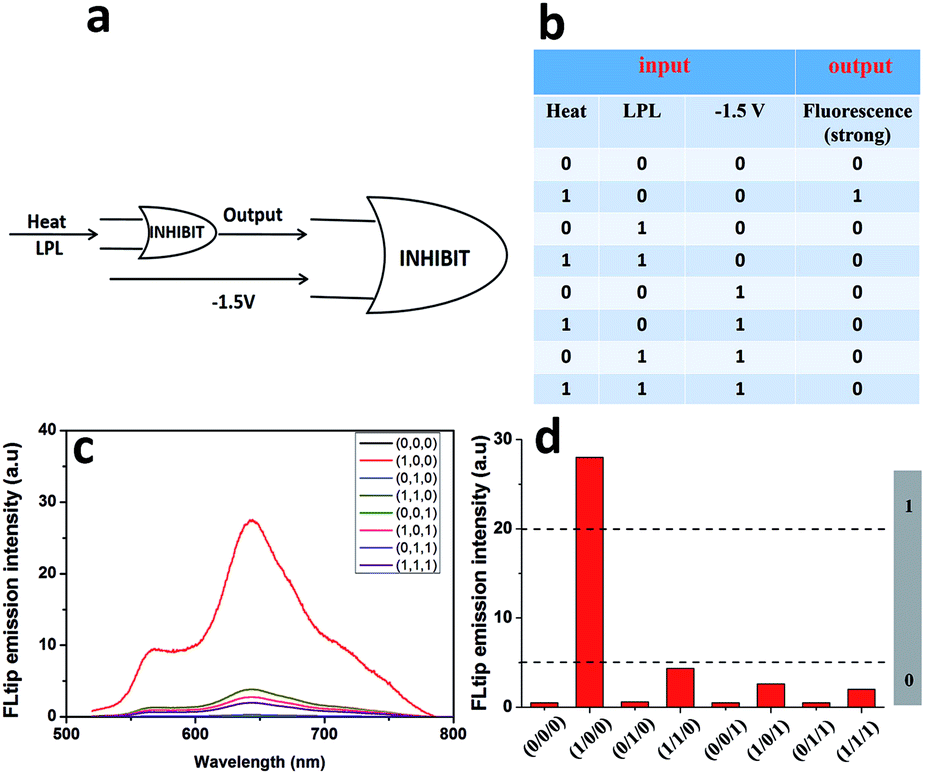
The integration of basic logic gates components is highly desirable, since it may provide an opportunity for the construction of more-complicated optoelectronic devices, promising new opportunities in integrated optical computing systems for future information technology.19–22 However, only a few reports concerning on the integration or concatenation between basic logic gates had been described.23–28 Herein, we constructed three-input logic gates by using above three triggers (thermal, electrical stimuli, and the polarization of the excited linearly polarized light) as the input signal and the tip emission of VFPDA microtube waveguide as the output signal. As shown in Fig. 6, we defined the “blue phase” VFPDA microtube (viologen units in MV+ state) as the initial state, and the strong tip emission as “1”, while weak tip emission as “0” with a threshold value of 5. A concatenated logic gate consisting of two concatenated INH gates could be realized when heating treatment, polarization of the excited linearly polarized light and electrical stimuli (−1.5 V) were served as input signals for the system. The presence and absence of heating treatment and electrical stimuli (−1.5 V) was defined as input “1” and “0”, respectively. The polarization of the excited linearly polarized light was defined as another inputs, and the polarization states 150° and 60° were defined as “1” and “0”, respectively. Before treatment (input 0/0/0), the tip emission of the VFPDA microtube was weak since PDA microtube matrix was in blue phase and the output signal was regarded as“0”. Upon applying heating treatment alone (input 1/0/0), PDA microtube transferred to red phase, and exhibited strong fluorescence (since viologen units in the MV2+ form, no FRET occurred). The fluorescence could be transported efficiently within the microtube since the polarization of the excited linearly polarized light (60°) was the same as the intrinsic alignment of PDA chains within the microtube matrix. Thus the tip emission was strong and the output signal was regarded as“1”. Upon applying the excitation with linearly polarized light (150°) alone (input 0/1/0), PDA microtube matrix was in blue phase and the output signal was regarded as“0”. Upon applying heating treatment and the excitation with linearly polarized light (150°) (input 1/1/0), PDA microtube transferred to red phase, and exhibited strong fluorescence. However, the fluorescence could be transported efficiently within the microtube since the polarization of the excited linearly polarized light (150°) was perpendicular to the intrinsic alignment of PDA chains within the microtube matrix. In this case, the tip emission of the VFPDA microtube remained weak (output 0). Upon applying the voltage of −1.5 V, viologen units transferred to blue MV+ form, and FRET between PDA microtube matrix and viologen units would occur if PDA microtube matrix transferred to the red phase upon treatment. In this case, the tip emission of the microtube would remained weak (output 0), regardless of other 2 inputs combinations (input 0/0/1, 0/1/1, 1/0/1, 1/1/1). Strong tip emission (output 1) could be detected only upon applying thermal stimuli alone (input 1/0/0, Fig. 6), suggesting that the system behaved as an INH–INH logic gate. Furthermore, for different starting condition or input combinations, various different concatenated logic gate (including AND–INH logic gate) operations could be achieved in single VFPDA microtube by similar mechanism (as shown Fig. S10†). All above results demonstrated that information could be transferred from one gate to the other by different stimulus and such concatenated logic gates of enhanced complexity would provide a higher versatility than single logic gates, which paved the way for constructing integrated more-complicated optical computing systems for future information technology.
 |
| | Fig. 6 (a) Scheme of the 3-input logic gates (INHIBIT–INHIBIT) based on the VFPDA microtube. (b) Truth table for the INHIBIT–INHIBIT gate. (c) Tip emission spectra of single VFPDA microtube of INHIBIT–INHIBIT gate with different combinations of the inputs upon excitation at 532 nm. (d) The fluorescence intensities of tip emission for the INHIBIT–INHIBIT logic gate. | |
Conclusions
In summary, a novel VFPDA microtubes have been designed and synthesized via thiol–ene based ‘click’ reaction, modulation of waveguide performance in single VFPDA microtube upon thermal, electrical stimuli, or the polarization of the excited linearly polarized light have been realized successfully. Various basic logic gates (AND, INH, NOR) and combinational logic circuits (INH–INH, AND–INH) were constructed successfully by using different starting condition or input combinations. The controllable switching of guided light in single VFPDA microtube and multiconfigurable logic gate operations may pave the way for the rational design of smart integrated optoelectronic devices for future optical computing and information technology.
Acknowledgements
This research was carried out with funding from the National Natural Science Foundation of China (51273186, 21574120, 91027024), the Chinese Academy of Sciences (kjcx2-yw-m11), the Basic Research Fund for the Central Universities (WK2060200012) and Science and Technological Fund of Anhui Province for Outstanding Youth (1608085J01).
Notes and references
- Q. Liao, H. B. Fu and J. N. Yao, Adv. Mater., 2009, 21, 4153 CrossRef CAS.
- J. Y. Zheng, Y. L. Yan, X. P. Wang, W. Shi, H. M. Ma, Y. S. Zhao and J. N. Yao, Adv. Mater., 2012, 24, OP194 CAS.
- S. M. Yoon, J. Lee, J. H. Je, H. C. Choi and M. Yoon, ACS Nano, 2011, 5, 2923 CrossRef CAS PubMed.
- H. Liu, J. B. Edel, L. M. Bellan and H. G. Craighead, Small, 2006, 2, 495 CrossRef CAS PubMed.
- D. O'Carroll, I. Lieberwirth and G. Redmond, Small, 2007, 3, 1178 CrossRef PubMed.
- V. Fasano, A. Polini, G. Morello, M. Moffa, A. Camposeo and D. Pisignano, Macromolecules, 2013, 46, 5935 CrossRef CAS PubMed.
- W. L. Hu, Y. K. Chen, H. Jiang, J. G. Li, G. Zou, Q. J. Zhang, D. G. Zhang, P. Wang and H. Ming, Adv. Mater, 2014, 26, 3136 CrossRef CAS PubMed.
- H. Y. Xia, Y. K. Chen, G. Yang, G. Zou, Q. J. Zhang, D. G. Zhang, P. Wang and H. Ming, ACS Appl. Mater. Interfaces, 2014, 6, 15466 CAS.
- D. J. Schmidt, F. C. Cebeci, Z. I. Kalcioglu, S. G. Wyman, C. Ortiz, K. J. Van Vliet and P. T. Hammond, ACS Nano, 2009, 8, 2207 CrossRef PubMed.
- X. F. Duan, Y. Huang, Y. Cui, J. F. Wang and C. M. Lieber, Nature, 2001, 409, 66 CrossRef CAS PubMed.
- J. C. Johnson, H. Q. Yan, R. D. Schaller, P. B. Petersen, P. D. Yang and R. J. Saykally, Nano Lett., 2002, 2, 279 CrossRef CAS.
- J. T. Hu, M. O. Yang, P. D. Yang and C. M. Lieber, Nature, 1999, 399, 48 CrossRef CAS.
- H. Kind, H. Q. Yan, B. Messer, M. Law and P. D. Yang, Adv. Mater, 2002, 14, 158 CrossRef CAS.
- J. C. Johnson, H. Q. Yan, R. D. Schaller, L. H. Haber, R. J. Saykally and P. D. Yang, J. Phys. Chem. B, 2001, 105, 11387 CrossRef CAS.
- A. B. Greytak, C. J. Barrelet, Y. Li and C. M. Lieber, Appl. Phys. Lett., 2005, 87, 151103 CrossRef.
- M. Liu, X. B. Yin, E. Ulin-Avila, B. S. Geng, T. Zentgraf, L. Ju, F. Wang and X. Zhang, Nature, 2011, 474, 64 CrossRef CAS PubMed.
- A. Reisch, M. D. Moussallem and J. B. Schlenoff, Langmuir, 2011, 27, 9418 CrossRef CAS PubMed.
- H. Y. Xia, R. X. Wang, Y. Y. Liu, J. J. Cheng, G. Zou, Q. J. Zhang, D. G. Zhang, P. Wang, H. Ming, R. Badugu and J. R. Lakowicz, Adv. Opt. Mater., 2015, 4, 371 CrossRef PubMed.
- F. Pu, E. G. Ju, J. S. Ren and X. G. Qu, Adv. Mater., 2014, 26, 1111 CrossRef CAS PubMed.
- X. W. He, Z. Li, M. Z. Chen and N. Ma, Angew. Chem., Int. Ed., 2014, 53, 14447 CrossRef CAS PubMed.
- S. J. Bradberry, J. P. Byrne, C. P. McCoy and T. Gunnlaugsson, Chem. Commun., 2015, 51, 16565 RSC.
- N. I. Georgiev, A. R. Sakr and V. B. Bojinov, Sens. Actuators, B, 2015, 221, 625 CrossRef CAS.
- L. Cai, S. M. Zhang, J. M. Miao, Z. B. Yu and C. Wang, Adv. Funct. Mater., 2015, 25, 5698 CrossRef CAS.
- F. M. Raymo, Adv. Mater., 2002, 14, 401 CrossRef CAS.
- J. Andreasson and U. Pischel, Chem. Soc. Rev., 2010, 39, 174 RSC.
- N. C. Gianneschi and M. R. Ghadiri, Angew. Chem., Int. Ed., 2007, 46, 3955 CrossRef CAS PubMed.
- M. Motornov, J. Zhou, M. Pita, V. Gopishetty, I. Tokarev, E. Katz and S. Minko, Nano Lett., 2008, 8, 2993 CrossRef CAS PubMed.
- A. Ogawa and M. Maeda, Chem. Commun., 2009, 4666 RSC.
Footnote |
| † Electronic supplementary information (ESI) available: 1H NMR spectrum, SEM results, fluorescence microscopy images, laser confocal microscopy images, scheme for modulation, FL microscopic images. See DOI: 10.1039/c6ra07564a |
|
| This journal is © The Royal Society of Chemistry 2016 |
Click here to see how this site uses Cookies. View our privacy policy here.