
UV-treated ZnO films for liquid crystal alignment
Jia-Wei Hua,
Sheng-Hsiung Yangb and
Shie-Chang Jeng*c
aInstitute of Photonics System, National Chiao Tung University, Tainan 711, Taiwan
bInstitute of Lighting and Energy Photonics, National Chiao Tung University, Tainan 711, Taiwan
cInstitute of Imaging and Biomedical Photonics, National Chiao Tung University, Tainan 711, Taiwan. E-mail: scjeng@faculty.nctu.edu.tw; Tel: +886 63032121
First published on 24th May 2016
Abstract
The surface wettability of ZnO films prepared by a sol–gel process is altered from hydrophobicity to hydrophilicity via ultraviolet (UV) light irradiation. The results indicate that hydrophilicity of the ZnO films is enhanced along with the increase of UV irradiation energy. The measurements of X-ray photoelectron spectroscopy and photoluminescence show that the amount of oxygen vacancies in ZnO films is increased with the UV irradiation. The results of UV-vis absorption spectroscopy and X-ray diffraction also show that the crystalline quality of the ZnO films is slightly changed after UV treatment. The increase in oxygen vacancies means that water molecules can easily coordinate into the oxygen vacancy sites, leading to the increase of surface wettability. It is observed that liquid crystal (LC) molecules can be aligned on the UV-treated ZnO films, and the orientation of LCs on the UV-treated ZnO films can be tuned from homeotropic to homogeneous alignment by controlling the surface wettability of ZnO films. Our results show that the pretilt angle of LCs on ZnO films depends on their surface wettability, and it can be successfully adjusted over a wide range from 89.5° to 0.5° as the contact angle of water on ZnO films changes from 97° to 60°.
1. Introduction
The electro-optical properties of LCDs strongly depend on the alignment films for orientating LC molecules. Conventionally, the mechanically buffed organic polyimide (PI) alignment films are applied to anchor the LC molecules with a specific orientation and pretilt angle, which is the angle between the director of the LC molecules and the alignment films. It is a mature technology in the LCD industry to use PI films for aligning LCs nearly parallel and perpendicular to the substrates using homogeneous PI and homeotropic PI, respectively.The technique for controlling pretilt angle is required for developing LC devices with different electro-optical properties, such as different LC displays modes1,2 and diffractive optical elements using inhomogeneous anchoring and pretilt angle.3 As a result, many methods have been developed to control the pretilt angle of LCs, such as polymer stabilization,4,5 mixture of different materials,6–8 and treatment of alignment films.9–12 Control of the pretilt angle of LCs has also been widely studied by adjusting the surface wettability of the alignment films.5,8,10,12–15 It is observed that a hydrophobic surface favors the homeotropic alignment and a hydrophilic surface favors the homogeneous alignment. Therefore, we can reasonably suppose that a film with controllable surface wettability can be applied for tuning the pretilt angle of the LC molecules.
Study of new alignment technologies is very important for academic and practical applications. Applications of inorganic ZnO films for aligning LCs are very promising for LCD systems operated in severe conditions, where a highly durable material is needed.16 Surface wettability of ZnO nanostructured films modified by photo irradiation have been reported.17,18 The wettability of ZnO films can be changed from hydrophobic surfaces to hydrophilic surfaces via ultraviolet (UV) irradiation. Besides, the ion beam (IB) bombardment on ZnO films as an alternative alignment approach has been reported by Seo's group.9,11 However, only a limited range of pretilt angle control (few degrees) was obtained.9,11 Recently, we found that the pretilt angle of LCs aligned on ZnO nanoparticle arrays can be controlled by annealing.12 However, the method cannot be applied to fabricate LCDs requiring patterned alignment films. The technique of photo alignment, irradiation of photon through a photo mask, can enable an area of alignment films to be divided into several domains with different alignment,19 which has found many applications, such as wide viewing angle LCDs,20 patterned retarders21 and LC lens.10
In this work, we applied UV treatment on ZnO films prepared by sol–gel process. The characteristics of UV-treated ZnO films were investigated by means of scanning electron microscope (SEM), atomic force microscopy (AFM), water contact angle (WCA) measurement, photoluminescence (PL) spectra, X-ray photoelectron spectroscopy (XPS), UV-vis absorption spectra, and X-ray diffraction (XRD). The UV-treated ZnO films were further applied as LC alignment films. The controllable pretilt angle of ZnO films can be achieved by using UV irradiation with different exposure times, which produce different surface wettability. The results show that the pretilt angle of LCs on ZnO films can be tuned over a wide range from 89.5° to 0.5° as the WCA on ZnO films changes from 97° to 60°.
2. Experimental methods
2.1 Materials
ZnO thin films were synthesized by the sol–gel method. A solution of zinc acetate dihydrate (0.22 g, 1 mmol) in 10 mL of isopropanol was stirred vigorously at 120 °C for 10 min. 2-(Dimethylamino)ethanol (0.089 g, 1 mmol) was slowly added to the above solution and stirred at the same temperature for an additional 2 h to form a homogeneous sol–gel solution. The solution was then spin-cast into a thin film on the ITO glass substrate at room temperature. The as-prepared thin film was annealed at 200 °C in air for 90 min to form the ZnO thin film, followed by UV exposure with different irradiation energy. The surface of the UV-treated ZnO alignment film was then subjected to rubbing treatment using a nylon cloth in such a way that the ZnO alignment film was rubbed once in each direction. The influence of UV treatment on ZnO films was conducted by irradiating the samples for the certain exposure times of 2, 4, 6, 8, 10, 12, and 14 min using an UV light (EXECURE 4000, HOYA) with a constant output intensity of 1.0 mW cm−2 measured by an UV radiometer (UVX-36, UVP).2.2 Sample preparation
To determine optical properties of LC molecules on UV-treated ZnO alignment films, antiparallel LC cells were assembled with the 5.5 μm Mylar films as the spacers. The LC cells were then filled with negative dielectric anisotropic LC molecules (Δε = −2.8, ε⊥ = 6.1, ne = 1.579, no = 1.483, Tc = 77 °C) at a temperature ∼100 °C for obtaining a uniform alignment. It is worth to note that the UV-treated ZnO films also show the similar alignment properties for using the positive dielectric anisotropic LC molecules, such as E7.2.3 Characterization
The morphology of the ZnO films was examined using SEM (SU8000, Hitachi) and AFM (Innova, Bruker). The PL measurement was conducted at room temperature by using a He–Cd laser for excitation (IK3301R-G, Kimmon). The PL and UV-vis absorption spectra were measured by a spectrometer (SP2150, Acton) and recorded by a photomultiplier tube (PD471, Princeton Instruments). Here, the 2.5 mmol sol–gel solution was applied to obtain a thick ZnO film for increasing PL signal. Electron spectra of ZnO films for chemical analysis were carried out by an XPS system (PHI 5000 Versa-Probe, PHI). The structure and crystallinity of ZnO was carried out by an XRD system (D/MAX-2500, Rigaku) using Cu-Kα radiation source (λ = 1.54 Å). Here, the 5.0 mmol sol–gel solution was applied to obtain a thick ZnO film for increasing XRD signal. The wettability of UV-treated ZnO films was evaluated by measuring the WCA on their surfaces using a contact angle analyzer (CAM-100, Creating Nano Technologies). The pretilt angles of LC cells were measured at room temperature by the modified crystal rotation method,22 where a laser interferometer (5530, Agilent) was used to determine the phase retardation.23 The optical properties of the LC cells were also evaluated by means of the polarizing optical microscope (POM).3. Results and discussion
The nanostructure and the morphology of the UV-treated ZnO films observed by SEM and AFM are shown in Fig. 1 and 2, respectively, where the sample without UV treatment is compared with the longest UV exposure time (14 min). The thickness and grain size of the ZnO films is around 50 and 58 nm, respectively as shown in Fig. 1. The roughness of the ZnO nanostructures is determined as ∼2 nm by AFM as shown in Fig. 2. No significant difference in morphology is observed for ZnO films before and after UV irradiation. | ||
| Fig. 1 SEM images of ZnO thin films (a) before and (b) after UV irradiation with an exposure time of 14 min. | ||
 | ||
| Fig. 2 AFM images of the ZnO film (a) before and (b) after the UV irradiation with an exposure time of 14 min. | ||
The results of WCA on the UV-treated ZnO thin films with different UV exposure time are shown in Fig. 3. It shows that the WCA decreases from 97° to 60° as the UV exposure time increases from 0 to 14 min. The results indicate that UV irradiation can mediate and increase the surface wettability of the ZnO films by increasing UV exposure time, while the ZnO surface is changed from hydrophobic to hydrophilic property. It is known that the wettability of a solid surface is determined by both the chemical property and the morphology of the surface. The morphology of ZnO films does not show any dependence on UV treatment as shown in Fig. 1 and 2; therefore, the further discussion that follows will center about the influence of UV irradiation on chemical properties of ZnO films.
 | ||
| Fig. 3 WCA of UV-treated ZnO films as a function of UV exposure time. | ||
The chemical composition of ZnO films relates to the defect chemistry and the surface crystal structure. It is reported ZnO has a rich and complicated defect property.24 Defects of ZnO films are intrinsic properties and highly depend on the synthetic process.24–28 Although the defect properties of ZnO materials have been intensive studied for more than 40 years, ZnO still has a controversy.24–28 The main defects in ZnO materials are zinc interstitial, oxygen vacancy and zinc vacancy. XPS was applied to evaluate the stoichiometry and defect property of UV-treated ZnO films as shown in Fig. 4. It illustrates the XPS survey spectra of treated-ZnO films before and after UV irradiation with an exposure time of 14 min. Clear photoelectron peaks from zinc and oxygen atoms in the binding energy region between 0 and 1200 eV are observed, such as Zn 2p, 3s, 3p, 3d, and O 1s signals.29 Besides, the O 1s signal can be further analyzed to provide additional information about different bonding types around oxygen atoms as shown in Fig. 5.17,30 This O 1s signal is composed of two components that correspond to different bonding environments of oxygen atoms existing in the UV-treated ZnO films.11,17,30 Firstly, the main binding component located at 530.1 eV corresponds to O2− ions in the ZnO lattice (Zn–O bonds) with hexagonal wurtzite structure. The amount of ZnO is expected to increase as the relative intensity of this signal is raised. Secondly, the shoulder component located around 531.5 eV is attributed to those O2− ions in the neighboring vacant oxygen sites, i.e. oxygen vacancies. The evolution of this shoulder signal reveals the change of oxygen vacancies in the ZnO films. According to the previous statement, the O 1s signal is resolved into two Gaussian-like curves centered at 530.1 and 531.5 eV as shown in Fig. 5. After UV exposure for 14 min, the relative intensity ratio of the main binding component from Zn–O bonds at 530.1 eV to total O 1s is decreased from 53.7% to 42.5%, indicating a decrease in the concentration of Zn–O bounds. Furthermore, it is noted that the shoulder component grows stronger from Fig. 5(a) and (b). The relative intensity ratio of the oxygen vacancies at 531.5 eV to total O 1s is increased from 46.3% to 57.5% after UV treatment. It is reported that UV irradiation generates electrons and holes in the ZnO lattice.17 Some of the holes react with lattice oxygen, leading to the formation of freely leaving oxygen molecules and defective sites on the surface of ZnO, so-called oxygen vacancies. Once these oxygen vacancies are formed, water molecules in air are consequently coordinated to those vacant sites and resulted in the increase of surface wettability, as shown previously in Fig. 3. Therefore, ZnO films provide photosensitive surfaces to be switched from hydrophobicity to hydrophilicity by UV irradiation.
 | ||
| Fig. 4 XPS survey spectra of ZnO films obtained before and after UV irradiation with an exposure time of 14 min. | ||
 | ||
| Fig. 5 High resolution O 1s XPS of ZnO films prepared (a) before and (b) after UV irradiation with an exposure time of 14 min. | ||
The defect properties of UV-treated ZnO films with different exposure times are also investigated by PL measurement as shown in Fig. 6, where three exposure times are plotted for comparison. The PL spectra of UV-treated ZnO films are featured by a strong ultraviolet (UV) emission near 380 nm from the free exciton recombination and a broad defect-related emission in the visible region.24–28 Specific energies of emission within the visible band have been assigned as a variety of defects in ZnO with different energies.24 The increased intensity of visible emissions with UV exposure time presented in Fig. 6 indicates that the concentration of point defect is increased.
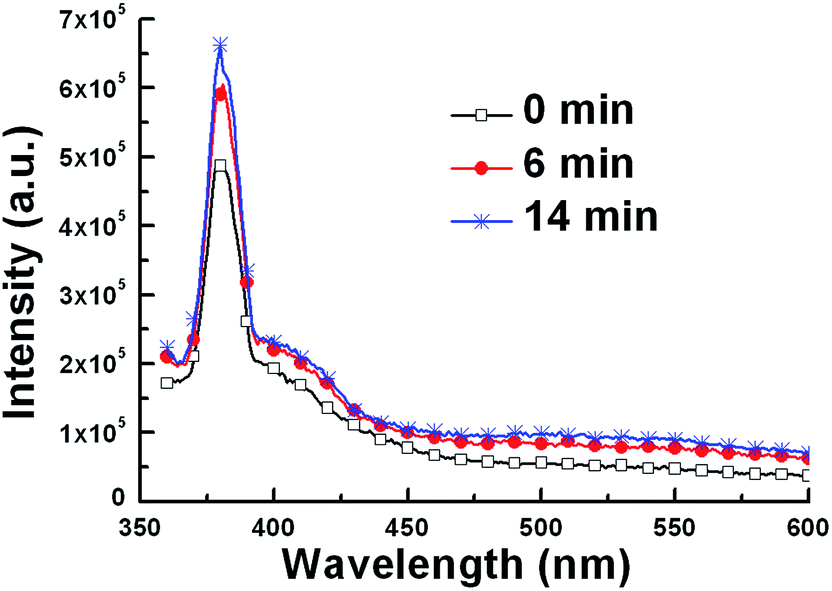 | ||
| Fig. 6 PL of UV-treated ZnO films with three different exposure times. | ||
The optical absorption spectra and band gap energy of ZnO films before and after UV irradiation with an exposure time of 14 min are also investigated as shown in Fig. 7 and 8, respectively. The optical absorption property is related to the fundamental energy gap, which depends on the properties of materials, such as the crystal structure31 and carrier concentration.32 For a semiconductor with a direct band gap, the energy band gap energy Eg can be estimated by the Tauc model: (αhν)2 = A(hν − Eg),33 where α is the absorption coefficient, A is a constant, hν is the photon energy of the incident light. The Eg is determined by extrapolating the tangential line to the photon energy axis in the plot of (αhν)2 versus hν as shown in Fig. 8. The Eg is then obtained as 3.30 eV and 3.32 eV for ZnO films before and after UV treatment, respectively. The slight change of Eg may indicate that the features of crystal structure and point defect of ZnO films are slightly changed with UV treatment.
 | ||
| Fig. 7 Absorbance spectra of ZnO films (a) before and (b) after UV irradiation with an exposure time of 14 min. | ||
 | ||
| Fig. 8 Optical band gap energy of ZnO films (a) before and (b) after UV irradiation with an exposure time of 14 min. | ||
The XRD results of as-prepared ZnO films on the glass substrate with different UV exposure times are shown in Fig. 9. The XRD patterns are identified by using the standard powder diffraction data of ZnO, referred at JCPDS file no. 36-1451. The XRD patterns show three main peaks at around 31.7°, 34.3°, and 36.3°. These peaks represent the existence of polycrystalline wurtzite structure of ZnO films. According to the XRD results, the average crystallite sizes D can be derived from the Scherrer's relation34 as D = 0.94λ/β![[thin space (1/6-em)]](https://www.rsc.org/images/entities/char_2009.gif) cosθ, where λ = 1.54 Å is the wavelength of the Cu-Kα radiation, β is the full width at half-maximum (FWHM) of the diffraction peak, and θ is the diffraction angle. The FWHM for ZnO films is determined as 1.04° and 0.94° for the (002) plane of ZnO films before and after UV irradiation with an exposure time of 14 min according to Fig. 9. The calculated crystallite size of ZnO thin films is changed from 9.7 to 10.3 nm after UV exposure. The slightly increased grain size in ZnO films indicates that the crystalline quality is slightly improved with UV treatment.
cosθ, where λ = 1.54 Å is the wavelength of the Cu-Kα radiation, β is the full width at half-maximum (FWHM) of the diffraction peak, and θ is the diffraction angle. The FWHM for ZnO films is determined as 1.04° and 0.94° for the (002) plane of ZnO films before and after UV irradiation with an exposure time of 14 min according to Fig. 9. The calculated crystallite size of ZnO thin films is changed from 9.7 to 10.3 nm after UV exposure. The slightly increased grain size in ZnO films indicates that the crystalline quality is slightly improved with UV treatment.
 | ||
| Fig. 9 XRD of ZnO films before and after UV irradiation with an exposure time of 14 min. | ||
Our XPS results in Fig. 5 are consistent with our PL results in Fig. 6, in which they both show that defects (oxygen vacancies) of ZnO films increase with UV exposure time. However, the geometrical structure of ZnO films still remains unchanged after UV exposure as shown in Fig. 1 and 2. It is well known that the surface chemistry and the surface roughness play an important role in the wetting properties of a solid surface, and the chemical composition of ZnO films relates to the defect chemistry and the surface crystal structure.35 Our studies confirm that the UV irradiation on the ZnO films brings about the generation of oxygen vacancies, which produces influence on the chemical composition and contributes to the formation of highly hydrophilic surfaces. The results of band gap energy in Fig. 8 and XRD in Fig. 9 also show that the crystallinity of ZnO films is slightly changed after UV treatment. The chemical properties of UV-treated ZnO films produce influence on the pretilt angle of LCs, which will be shown later.
The pretilt angle of LCs and WCA on ZnO films for different UV exposure times are both shown in Fig. 10. The pretilt angle decreases from 89.5 to 0.5° as the CA of water decreases from 97° to 60°. Both the pretilt angle and the WCA decrease as the UV exposure time increases. The results confirm that the pretilt angle of LCs on the UV-treated ZnO film strongly depends on its surface wettability, and the pretilt angle of the ZnO film can be easily controlled by exposure time of UV irradiation. The relationship between the surface wettability and pretilt angle of an alignment film has been widely investigated.5,8,10,12–15,36 An alignment film with more polar surfaces gives a lower pretilt angle due to the increased interaction between LC molecules and the alignment film.13,14,36
 | ||
| Fig. 10 Pretilt angle of LCs and WCA on ZnO film as a function of UV exposure time. | ||
The POM photographs of antiparallel LC cells with UV-treated ZnO alignment films with different exposure times are shown in Fig. 11. The transmission of LC cells changes from dark state (0 min, pretilt angle ∼89.5°) to bright state (14 min, pretilt angle ∼0.5°). The LC cells with different color represent the different pretilt angles corresponding to the different phase retardations. These results agree with the results shown in Fig. 10.
 | ||
| Fig. 11 POM photographs of antiparallel LC cells with UV-treated ZnO alignment films with different UV exposure times: (a) 0, (b) 2, (c) 4, (d) 6, (e) 8, (f) 10, (g) 12, and (h) 14 min. | ||
The stability of alignment materials under the high temperature and photo illumination environments are important for LCDs' applications. Recently, photostability of organic PI and inorganic silicon-dioxide (SiO2) alignment films were studied and compared by C.-H. Wen et al.16 Their results indicated that SiO2 alignment films are superior than conventional PI films under severe conditions. In order to study the reliability of UV-treated ZnO alignment films unambiguously, the contamination produced by the rubbing process should be avoided.37 We are developing several non-rubbing methods37 and the stability of the as-prepared ZnO films under severe conditions will be evaluated in the near future.
4. Conclusions
In conclusion, we have applied UV treatment on ZnO films prepared by sol–gel process. The UV-treated ZnO films were further applied as LC alignment films. The controllable pretilt angle of LCs on ZnO films can be obtained by different UV exposure times. The results of XPS and PL have shown that the chemical compositions of ZnO films have been changed with the UV irradiation, which produce influence on the surface wettability. The results of band gap energy and XRD measurements also show that the crystallinity of ZnO films is slightly changed after UV treatment. Our results show that the pretilt angle of LCs on ZnO films depends on their surface wettability, and it can be successfully adjusted over a wide range from 89.5° to 0.5° as the WCA on ZnO films changes from 97° to 60°. Our proposed method of making inorganic ZnO alignment films with tunable pretilt angles is very simple and easy for scale-up production in the current LCD industry.Acknowledgements
We thank the anonymous reviewers for their constructive comments. The authors thank the Ministry of Science and Technology of Taiwan for financially supporting this research under contract MOST 103-2112-M-009-013-MY3, and NSC102-2113-M-009-007.Notes and references
- F. S. Yeung and H.-S. Kwok, Appl. Phys. Lett., 2006, 88, 063505 CrossRef.
- X. J. Yu and H.-S. Kwok, Appl. Phys. Lett., 2004, 85, 3711–3713 CrossRef CAS.
- S. Valyukh, V. Chigrinov, H.-S. Kwok and H. Arwin, Opt. Express, 2012, 20, 15209–15221 CrossRef CAS PubMed.
- T. J. Chen and K. L. Chu, Appl. Phys. Lett., 2008, 92, 091102 CrossRef.
- B.-Y. Liu and L.-J. Chen, J. Phys. Chem. C, 2013, 117, 13474–13478 CAS.
- H.-S. Kwok and F. S. Y. Yeung, J. Soc. Inf. Disp., 2008, 16, 911–918 CrossRef CAS.
- D. Ahn, Y.-C. Jeong, S. Lee, J. Lee, Y. Heo and J.-K. Park, Opt. Express, 2009, 17, 16603–16612 CrossRef CAS PubMed.
- S.-J. Hwang, S.-C. Jeng and I.-M. Hsieh, Opt. Express, 2012, 18, 16507–16512 CrossRef PubMed.
- B.-Y. Oh, W.-K. Lee, Y.-H. Kim and D.-S. Seo, J. Appl. Phys., 2009, 105, 054506 CrossRef.
- S.-C. Jeng, S.-J. Hwang, J.-S. Horng and K.-R. Lin, Opt. Express, 2010, 18, 26325 CrossRef CAS PubMed.
- J. J. Lee, H. G. Park, J. J. Han, D. H. Kim and D. S. Seo, J. Mater. Chem. C, 2013, 1, 6824 RSC.
- Y.-F. Cheng, M.-Z. Chen, S.-H. Yang and S.-C. Jeng, ACS Appl. Mater. Interfaces, 2015, 7, 9619 Search PubMed.
- S.-H. Paek, C. J. Durning, K.-W. Lee and A. Lien, J. Appl. Phys., 1998, 83, 1270–1280 CrossRef CAS.
- B. S. Ban and Y. B. Kim, J. Appl. Polym. Sci., 1999, 74, 267–271 CrossRef CAS.
- H. J. Ahn, J. B. Kim, K. C. Kim, B. H. Hwang, J. T. Kim, H. K. Baik, J. S. Park and D. Kang, Appl. Phys. Lett., 2007, 90, 253505 CrossRef.
- C.-H. Wen, S. Gauza and S.-T. Wu, J. Soc. Inf. Disp., 2005, 13, 805–811 CrossRef CAS.
- R. D. Sun, A. Nakajuma, A. Fujishima, T. Watanabe and K. Hashimoto, J. Phys. Chem. B, 2001, 105, 1984–1990 CrossRef CAS.
- X. Feng, L. Feng, M. Jin, J. Zhai, L. Jiang and D. Zhu, J. Am. Chem. Soc., 2004, 126, 62–63 CrossRef CAS PubMed.
- V. G. Chigrinov, V. M. Kozenkov and H.-S. Kwok, Photoalignment of Liquid Crystalline Materials: Physics and Applications, John Wiley & Sons Ltd, England, 2008 Search PubMed.
- M. Schadt, H. Seiberle and A. Schuster, Nature, 1996, 381, 212–215 CrossRef CAS.
- P. V. Witte, M. Brehmer and J. Lub, J. Mater. Chem., 1999, 9, 2087–2094 RSC.
- K.-H. Chen, W.-Y. Chang and J.-H. Chen, Opt. Express, 2009, 17, 14143–14149 CrossRef CAS PubMed.
- S. J. Hwang, J. Disp. Technol., 2005, 1, 77–81 CrossRef CAS.
- M. D. McCluskey and S. J. Jokela, J. Appl. Phys., 2009, 106, 071101 CrossRef.
- D. C. Iza, D. Munoz-Rojas, Q. Jia, B. Swartzentruber and J. L. MacManus-Driscoll, Nanoscale Res. Lett., 2012, 7, 655 CrossRef PubMed.
- L. E. Greene, M. Law, D. H. Tan, M. Montano, J. Goldberger, G. Somorjai and P. Yang, Nano Lett., 2005, 5, 1231–1236 CrossRef CAS PubMed.
- N. Shakti, A. Prakash, T. Mandal and M. Katiyar, Mater. Sci. Semicond. Process., 2014, 20, 55–60 CrossRef CAS.
- D. Li, Y. H. Leung, A. B. Djurisic, Z. T. Liu, M. H. Xie, S. L. Shi and S. J. Xu, Appl. Phys. Lett., 2004, 85, 1601–1603 CrossRef CAS.
- A. Naumkin, A. Kraut-Vass, S. W. Gaarenstroom, and C. J. Powell, NIST X-ray Photoelectron Spectroscopy Database, accessed May, 2015, http://srdata.nistgov/xps/ Search PubMed.
- S. Major, S. Kumar, M. Bhatnagar and K. K. Chopra, Appl. Phys. Lett., 1986, 49, 394–396 CrossRef CAS.
- R. Dalven, Phys. Rev. B, 1973, 8, 6033 CrossRef CAS.
- S. Cho, Transactions on Electrical and Electronic Materials, 2009, 10, 185 CrossRef.
- F. Yakuphanoglu, M. Sekerci and O. F. Ozturk, Opt. Commun., 2004, 239, 275 CrossRef CAS.
- B. D. Cullity, Elements of X-ray diffraction, Addison-Wesley, Reading, 1979 Search PubMed.
- P. C. Hiemenz and R. Rajagopalan, Principles of Colloid and Surface Chemistry, Marcel Dekker, Inc., New York, 1997 Search PubMed.
- H.-Y. Wu, C.-Y. Wang, C.-J. Lin, R.-P. Pan, S.-S. Lin, C.-D. Lee and C.-S. Kou, J. Phys. D: Appl. Phys., 2009, 42, 155303 CrossRef.
- K. Takatoh, M. Hasegawa, M. Koden, N. Itoh, R. Hasegawa and M. Sakamoto, Alignment Technologies and Applications of Liquid Crystal Devices, Taylor & Francis, Oxon, 2005 Search PubMed.
| This journal is © The Royal Society of Chemistry 2016 |