DOI:
10.1039/C6RA07443J
(Paper)
RSC Adv., 2016,
6, 58733-58739
Ferroelectric-like hysteresis effect observed in carbon quantum dots sandwiched between PMMA and PEDOT:PSS hybrid film
Received
22nd March 2016
, Accepted 11th June 2016
First published on 14th June 2016
Abstract
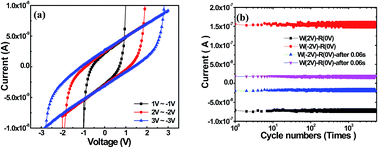
The ferroelectric-like hysteretic I–V effect was observed in the multilayer film of PMMA/carbon quantum dot (CD)/PEDOT:PSS using ITO and Al metal as the electrodes. The multilayer film exhibited two different resistance states and larger hysteresis window under the electric field compared to the film without CD addition. The influence of additional CD layers on the short circuit current (Isc) and open circuit voltage (Voc) values is related to the interfacial polarization between PMMA and PEDOT:PSS layers. The introduction of a CD layer intensifies interfacial polarization for two dielectric layers, resulting in the larger hysteresis window. An interfacial polarization field E′ increases with the external electric field increasing and reaches a maximum value at the threshold voltage Voc of ±15 V. The switch reliability of the device is operated over 5 × 10³ times in a succession of periodic pulses without any performance degradation.
1. Introduction
Electrical bistable memory devices (EBMDs) based on hybrid organic–inorganic nanocomposites have emerged as excellent candidates for promising application in next-generation memory devices owing to their low fabrication cost and power consumption, good compatibility with semiconductor logic processes and tolerance towards flexible substrates.1–7 As active layers in the devices, various nanoparticles including metal nanoparticles,8 metal oxide semiconductors,9 and the new-fashioned carbon family3,10–16 have been conceived and employed. Carbon quantum dots (CDs) have exhibited tunable photoluminescence (PL) spectra, broad light absorption, water solubility, nontoxicity and excellent biocompatibility.17 CDs have drawn considerable attention to the possible application in photochemical catalysis,18 energy conversion/storage,19 light-emitting devices,20 biological and medical engineering,21 etc. Numerous surface functional groups in CDs permit them easily to hybrid with polymer or inorganic materials to improve the device performance. For examples, Lan et al. found CDs-decorated polymer UMCM-1 have a positive effect on H2 storage capacity for adsorption interaction between polar functional groups (such as –COOH and –OH) at the CDs surface and H2 molecules.22 Briscoe et al. reported the performance of solid-state nanostructured solar cells based on biomass-derived CDs sensitized ZnO nanorods is distinctly dependent on surface functional groups of the CDs.23 In the polymer-based EBMDs, PEDOT:PSS and PMMA are mostly selected as memory media because of their fundamental chemistry and physics. In the memory mechanism investigations, insulating polymer PMMA is generally considered as barrier layer for preventing the carriers escaping1,12,16 and PEDOT:PSS is usually taken as memory unit. Forrest et al. revealed that the phase segregation of the conducting PEDOT+ and the insulating PSS− chains in high electric field and high temperature lead to the memory behavior of the PEDOT:PSS-based device.24 In addition, the oxidation and the reduction of the PEDOT:PSS layer for the electrons injection and release play important role in the state switching.25–27
As the polar molecules, PEDOT:PSS and PMMA are typically polarized by an external electric field.28,29 The abundant functional groups of CDs can be responsible to interact with polymer molecules and then have the effect on interfacial polarization in electric field. In this work, the multilayer film of PMMA/CDs/PEDOT:PSS is used as an active layer in the EBMD. A ferroelectric-like hysteretic I–V characteristic was found with a large memory window and the reliable stability for the loop voltage switching over 5 × 10³ times was simultaneously obtained. The memory mechanism was discussed based on the polar molecules PEDOT:PSS and PMMA and was explained in terms of intensified interfacial polarization by the additional introduction of CDs layer.
2. Experimental details
The aqueous solution of PEDOT:PSS (Clevios P VP Al 4083, Net: 0.25 kg = 0.25 L) was provided by Germany Heraeus Company, and the PMMA was purchased from Aladdin Reagent Corporation (Shanghai, China). As described by the literature,30 the CDs were synthesized with octadecylamine and citric acid anhydrous as precursor in 1-octadecene noncoordinating solvent. Briefly, 15 mL 1-octadecene and the 1.5 g octadecylamine were added to a 100 mL three-neck flask under Ar atmosphere. When the temperature was up to 270 °C, 1 g citric acid was quickly added into the flask under vigorous stirring and maintained for 15 min. The final products were repeatedly purified with acetone as a precipitating agent and then the 0.1 g as-obtained CDs were dissolved in 5 mL toluene solvent. Meanwhile, the cleaned ITO coated glass substrates by ultrasonication in detergent, distilled water, acetone, isopropanol and methanol in succession were dried at 80 °C in vacuum for 3 h and then treated by UV-ozone radiation for 15 min. To assemble the EBMD, 0.3 mL original PEDOT:PSS was deposited on ITO substrates by spin-coating at 700 rpm for 20 s and 4000 rpm for 45 s. Then, 0.3 mL CDs toluene solvent was coated onto the PEDOT:PSS layer at 700 rpm for 20 s and 2000 rpm for 30 s. After that, 0.3 mL PMMA/trichloromethane solution coating at the concentration of 4 mg mL−1 was performed on the CDs layer at 700 rpm for 20 s and 2500 rpm for 45 s. The vacuum drying at 80 °C for 1 h in every step was used to remove the residual solvents. Finally, Al top electrode with thickness of 130 nm was deposited by using thermal evaporation through a metal mask. The effective area corresponding to the overlapping area of bottom (ITO) and top electrode (Al) is 4 mm2. Fig. 1 shows the device schematic structure of Al/PMMA/CDs/PEDOT:PSS/ITO, the molecular structures of polymer PMMA and PEDOT:PSS and the cross-sectional field emission scanning electron microscopy (FESEM) image of the hybrid film. With the same preparation condition, a device structure of Al/PMMA/PEDOT:PSS/ITO was obtained.
 |
| | Fig. 1 The (a) schematic diagrams of the Al/PMMA/CDs/PEDOT:PSS/ITO device, molecular structures of PMMA and PEDOT:PSS and (b) cross-sectional SEM image of the hybrid film. | |
The Fourier transform infrared (FTIR) spectrometer (Bruker Tensor 27) was used to investigate the surface functional groups of as-fabricated CDs film in the wavenumber region 400 cm−1 to 4000 cm−1 by transmission mode. The Raman spectrum (Thermo Fisher DXR Raman Microscope) with a 532 nm excitation wavelength was carried out to feature the characteristic bands of the CDs film and hybrid film. The hybrid film for Raman measurements were prepared in the same preparation process as the active layer in the device. PL spectra of CDs solutions were obtained on the spectrometer (FluoroLog 3, Horiba Jobin Yvon) using 450 W Xe lamp. The morphology of the hybrid film was investigated by SEM (Hitachi SU-8010). The I–V characteristics and endurance tests of devices were performed by the keithley 2400 digital source meter. In the electrical characteristics, the top Al electrode was grounded and the bias voltage was applied to the bottom ITO electrode. All the measurements were carried out at room temperature without encapsulation.
3. Results and discussion
The FTIR spectrum of as-fabricated CDs film is shown in Fig. 2(a). The peak position at the 1640 cm−1 associates with stretching vibration of –CONH group. The typical peak at 1707 cm−1 is related to carboxyl C
O vibration, and the band between 2980 and 2765 cm−1 belongs to the –CH2–/–CH3 stretch of the carbon skeleton. The low energy bands corresponding to 3980 cm−1 and 3400–3130 cm−1 are representing the stretching vibration of –NH– and –OH, respectively.31,32 Fig. 2(b) shows the Raman spectra of as-fabricated CDs film and hybrid film. The peaks at 1350 cm−1 and 1600 cm−1 of both films can be attributed to D-band and G-band of CDs, respectively. According to reported literature, G-band is originated from sp2 carbon skeleton and D-band from sp3 carbon. The strong intensity of D-band indicates that the bad crystalline quality of carbon networks with the disorder and defects.33 The amount of functional groups may exist on the surface of CDs. For the Raman spectra of hybrid film, the peak at 1442 cm−1 is related to C
C symmetrical stretching vibration, and the two peaks centered at 1508 cm−1 and 1570 cm−1 are corresponding to the C
C asymmetric stretching vibrations of thiophene rings from PEDOT:PSS.34 The peaks located at 2806 cm−1 and 2902 cm−1 represent the combination band involving O–CH3 and νs(C–H) from PMMA.35 The PL spectra of CDs toluene solution are shown in Fig. 2(c). The red-shift in emission peak position as the excitation energy decrease is commonly regarded as the indicative of the various surface states and size distribution.3,18,20,30 Based on the above analysis, the preparation process for CDs and their chemical structure are briefly described in Fig. 2(d).
 |
| | Fig. 2 The (a) FTIR spectrum of as-fabricated CDs film, (b) Raman spectra of as-fabricated CDs film and hybrid film, (c) the PL spectra of CDs solution and (d) the preparation process and the chemical structure of as-synthesized CDs. | |
Fig. 3(a) shows the I–V curves of the device Al/PMMA/CDs/PEDOT:PSS/ITO in the multiple-valued voltages which are conducted from +1 V to −1 V, +2 V to −2 V and +3 V to −3 V, respectively. No obvious switch voltage was observed in comparison to previous reports,1,3,4 but the hysteresis-like loop with two resistance states distinctly occurs. The semi-log curves corresponding to Fig. 3(a) are plotted in Fig. 3(b). A short circuit current value (Isc) is obtained at zero-bias when the voltage goes through 0 V at both forward and reverse sweeping, which is not a common feature. And the Voc (open circuit voltage value when the device current is zero) also exhibits similar behavior. As suggested in the previous paper,28 the interfacial polarization between dielectric polymers can takes place on application of an electric field (E0) due to higher molecular spatial ordering. The values of Isc, whose direction is contrary to the external electric field E0, are originated from the polarization field (E′). A saturation value for Isc and Voc can be observed when the applied voltage is increased up to ±15 V, as shown in Fig. 3(c) and (d). It is regarded as threshold field in the ref. 36 and indicates the polarization saturation.
 |
| | Fig. 3 (a) The linear I–V curves in the cyclic multiple-valued voltage sweeping from +1 V to −1 V, +2 V to −2 V and +3 V to −3 V for the device Al/PMMA/CDs/PEDOT:PSS/ITO, respectively. (b) The corresponding semi-log plots of (a). (c) The semi-log I–V curves when the voltage range increase from ±3 V to ±15 V. (d) The Voc as functions of different loop voltages. The ‘5 V’ on the horizontal axis represents the loop voltage scanning from −5 V to 5 V, the ‘−5 V’ is from 5 V to −5 V. | |
The I–V curves in Fig. 4 are obtained by a deliberate break at zero-bias. It is obviously noticed that Isc discontinuously transit from the non-zero value to initial zero value at the break site as the arrow marked in Fig. 4(a) and the feature is not affected by the sweeping range and the cycle numbers. The phenomenon is attributed to the vanishing polarization field E′. Spatial ordering of the molecules is disorganized and get back to random orientation in the interface.
 |
| | Fig. 4 (a)–(c) The I–V curves by a deliberate break at zero-bias for voltage sweeping from +1 V to −1 V, +2 V to −2 V and +3 V to −3 V, respectively. | |
The device operated in multiple cycles demonstrates the switch reliability, as shown in Fig. 5(a). Be driven by applied voltage in pulse-periodic mode of −2 V(−1 V) → 0 V → +2 V(+1 V) → 0 V over 5 × 10³ times, the device is repeatedly switched between two independent states with stable current value at the “read” voltage of 0 V. Simultaneously, the flow of current is found to be reverse to the applied electric field E0, supporting the existence of polarization field E′. And the Isc value at the write voltage of ±2 V is higher than that at ±1 V, which is induced by the high polarized electric field E′. At the same absolute applied voltage, the different absolute value of current at the forward and reverse electric field was observed, implying that there is a difference in contact resistance or a Schottky-like barrier.36,37 Fig. 5(b) shows the Isc values measured at t = 0 s and 0.06 s at the write voltage of 2 V and read voltage of 0 V. The reduced Isc value at 0.06 s is reasonable related to the decreasing polarization field E′ for disorganized polarization. The Isc value will be closed to zero due to the gradually disappeared E′ as the time extend.
 |
| | Fig. 5 (a) The switch reliability by applied voltage in pulse-periodic mode of −2 V(−1 V) → 0 V → +2 V(+1 V) → 0 V. (b) The Isc values measured at t = 0 s and 0.06 s at the write voltage of 2 V and read voltage of 0 V. | |
Compared to the reference device without CDs layer, the device with PMMA/CDs/PEDOT:PSS hybrid film shows an enlarged memory window with a larger Isc and Voc values at the forward and reverse sweeping, as shown in Fig. 6(a) and (b), which can be attributed to the enhanced spatial ordering of electric dipole moments between the interfaces PMMA and CDs as well as PEDOT:PSS and CDs under the applied external field E0. The detail schematic diagrams for hysteresis mechanisms of two devices are shown in Fig. 7. The molecular orientation of polar molecule PMMA and PEDOT:PSS has a strong electric field dependence.38 As indicated in Fig. 7(a), the electric dipole moments of all molecules for two dielectric PEDOT:PSS and PMMA are randomly arranged in absence of external electric field E0. When an the external electric field E0 is applied on the device, the orientations of molecules' electric dipole moments are mostly parallel to the direction of the E0, as shown in Fig. 7(b). An interfacial polarization field E′ induced by the polarization charges of two dielectric layers increases with the external electric field increasing and reaches a maximum value at the threshold voltage Voc of ±15 V. When the field E0 decreases return to zero, the device current is mainly determined by the polarization field E′.11 The E′ originating from the dipole–dipole interaction between PEDOT:PSS and PMMA for the reference device Al/PMMA/PEDOT:PSS/ITO induces a ferroelectric-like hysteresis effect (Fig. 7(c)). Incorporation of CDs can intensify dipole–dipole interaction between the negative –OH group in CDs and positive PEDOT+ of the PEDOT:PSS and between –NH group in CDs and –OCH3 in PMMA due to the different polarity of functional groups. The increased electric dipole moment and their enhanced spatial ordering in sandwiched multilayer can increase the polarization electric field E′ (see Fig. 7(d)), which can enlarge memory window with obvious Isc and Voc values. Similar hysteresis like I–V characteristics was observed in ethanol adsorbed ZnO nanorods related to the formation of dipole charges of adsorbed ethanol molecules on the ZnO nanorods surface.36
 |
| | Fig. 6 (a) The linear I–V curves and (b) plotted semi-log I–V curves for the device Al/PMMA/CDs/PEDOT:PSS/ITO and device Al/PMMA/PEDOT:PSS/ITO. | |
 |
| | Fig. 7 The detail schematic diagrams for hysteresis mechanisms. (a) The molecular orientation of polar molecule PMMA and PEDOT:PSS in absence of external electric field E0. (b) The molecular orientation of PMMA and PEDOT:PSS under the electric field E0. (c) and (d) The molecular orientation of PMMA and PEDOT:PSS without and with the CDs addition with the electric field E0 removed. | |
The previous study revealed that the defects in CDs acting as electron trapping centers play a major role in the bistable properties of the devices. In this work, no such bistable behavior was observed for the device with monolayer CDs film. The contribution of the electron capturing by the CDs defects for the better memory performance is not the primary factor. Further experiment will be carried out to investigate the role of the CDs defects in such a device. Overall, it is effective way to improve the performance of the memory device with the ferroelectric-like hysteresis effect by incorporation of the sandwiched polarization medium.
4. Conclusions
The devices of Al/PMMA/CDs/PEDOT:PSS/ITO and Al/PMMA/PEDOT:PSS/ITO have been fabricated using a simple spin-coating method. The devices show a ferroelectric-like hysteretic I–V characteristic due to interfacial polarization in hybrid films. The polarization charges can form an additive reverse field E′ and produce a nonzero current Isc at zero-bias and Voc at zero-current. The values of Isc and Voc increase with the applied field E0 increasing and the saturation values are obtained at the threshold field ±15 V. The device with additional CDs layer shows an enlarged window, which is attributed to the enhanced spatial ordering of electric dipole moments between PMMA and CDs as well as PEDOT:PSS and CDs under applied external field E0. The switch reliability of device is operated over 5 × 10³ times in a succession of periodic pulses without any performance degradation.
Acknowledgements
This work was supported by the National High Technology Research and Development Program of China (863 Program) (Grant No. 2013AA014201), the Natural Science Foundation of Tianjin (Grant Nos 14JCZDJC31200, 15JCYBJC16700 and 15JCYBJC16800), the National Key Foundation for Exploring Scientific Instrument of China (Grant No. 2014YQ120351) and International Cooperation Program from Science and Technology of Tianjin (Grant No. 14RCGHGX00872).
References
- D. Y. Yun, N. S. Arul, D. U. Lee, N. H. Lee and T. W. Kim, Org. Electron., 2015, 24, 320–324 CrossRef CAS.
- C. Tan, Z. Liu, W. Huang and H. Zhang, Chem. Soc. Rev., 2015, 44, 2615–2628 RSC.
- L. Meng, M. Lan, L. Guo, L. S. Xie, H. Wang, J. Ge, W. Liu, Y. Wang and P. Wang, RSC Adv., 2015, 5, 26886–26890 RSC.
- Z. Ma, C. Wu, D. U. Lee, F. Li and T. W. Kim, Org. Electron., 2016, 28, 20–24 CrossRef CAS.
- R. A. Nawrocki, E. M. Galiger, D. P. Ostrowski, B. A. Bailey, X. Jiang, R. M. Voyles, N. Kopidakis, D. C. Olson and S. E. Shaheen, Org. Electron., 2014, 15, 1791–1798 CrossRef CAS.
- L. Liang, K. Li, C. Xiao, S. Fan, J. Liu, W. Zhang, W. Xu, W. Tong, J. Liao, Y. Zhou, B. Ye and Y. Xie, J. Am. Chem. Soc., 2015, 137, 3102–3108 CrossRef CAS PubMed.
- B. Sun, Y. Liu, W. Zhao and P. Chen, RSC Adv., 2015, 5, 13513–13518 RSC.
- C. O. Baker, B. Shedd, R. J. Tseng, A. A. Martinez-Morales, C. S. Ozkan, M. Ozkan, Y. Yang and R. B. Kaner Baker, ACS Nano, 2011, 5, 3469–3474 CrossRef CAS PubMed.
- F. Yang, M. Wei and H. Deng, J. Appl. Phys., 2013, 114, 134502–134507 CrossRef.
- S. ChandraKishore and A. Pandurangan, RSC Adv., 2014, 4, 9905–9911 RSC.
- S. Paul, A. Kanwal and M. Chhowalla, Nanotechnology, 2006, 17, 145–151 CrossRef CAS.
- D. I. Son, T. W. Kim, J. H. Shim, J. H. Jung, D. U. Lee, J. M. Lee, W. I. Park and W. K. Choi, Nano Lett., 2010, 10, 2441–2447 CrossRef CAS PubMed.
- Q. Zhang, J. Pan, X. Yi, L. Li and S. Shang, Org. Electron., 2012, 13, 1289–1295 CrossRef CAS.
- C. Wu, F. Li, T. Guo and T. W. Kim, Org. Electron., 2012, 13, 178–183 CrossRef CAS.
- D. Y. Yun, H. M. Park, S. W. Kim, S. W. Kim and T. W. Kim, Carbon, 2014, 75, 244–248 CrossRef CAS.
- L. Kou, F. Li, W. Chen and T. Guo, Org. Electron., 2013, 14, 1447–1451 CrossRef CAS.
- S. C. Ray, A. Saha, N. R. Jana and R. Sarkar, J. Phys. Chem. C, 2009, 113, 18546–18551 CrossRef CAS.
- H. Ming, Z. Ma, Y. Liu, K. Pan, H. Yu, F. Wang and Z. Kang, Dalton Trans., 2012, 41, 9526–9531 RSC.
- L. Cao, S. Sahu, P. Anilkumar, C. E. Bunker, J. Xu, K. A. S. Fernando, P. Wang, E. A. Guliants, K. N. Tackett and Y. P. Sun, J. Am. Chem. Soc., 2011, 133, 4754–4757 CrossRef CAS PubMed.
- F. Wang, Y. H. Chen, C. Y. Liu and D. G. Ma, Chem. Commun., 2011, 47, 3502–3504 RSC.
- W. Bai, H. Zheng, Y. Long, X. Mao, M. Gao and L. Zhang, Anal. Sci., 2011, 27, 243–246 CrossRef CAS PubMed.
- J. Li, Y. Tang, S. Li, S. Zhang, Z. Dai, L. Si and Y. Lan, CrystEngComm, 2015, 17, 1080–1085 RSC.
- J. Briscoe, A. Marinovic, M. Sevilla, S. Dunn and M. Titirici, Angew. Chem., Int. Ed., 2015, 54, 4463–4468 CrossRef CAS PubMed.
- X. Xu, R. A. Register and S. R. Forrest, Appl. Phys. Lett., 2006, 89, 142109 CrossRef.
- H. Ha and O. Kim, Appl. Phys. Lett., 2008, 93, 033309 CrossRef.
- J. A. Ávila-Niño, E. Segura-Cárdenas, A. O. Sustaita, I. Cruz-Cruz, R. López-Sandoval and M. Reyes-Reyes, Mater. Sci. Eng., B, 2011, 176, 462–466 CrossRef.
- J. M. Son, W. S. Song, C. H. Yoo, D. Y. Yun and T. W. Kim, Appl. Phys. Lett., 2012, 100, 183303 CrossRef.
- J. Mangalam, S. Agarwal, A. N. Resmi, M. Sundararajan and K. B. Jinesh, Org. Electron., 2016, 29, 33–38 CrossRef CAS.
- S. A. Odhiambo, G. De Mey, C. Hertleer, A. Schwarz and L. Van Langenhove, Text. Res. J., 2014, 84, 347–354 CrossRef.
- F. Wang, S. Pang, L. Wang, Q. Li, M. Kreiter and C. Liu, Chem. Mater., 2010, 22, 4528–4530 CrossRef CAS.
- X. Han, S. Zhong, W. Pan and W. Shen, Nanotechnology, 2015, 26, 065402 CrossRef CAS PubMed.
- S. Do, W. Kwon and S. W. Rhee, J. Mater. Chem. C, 2014, 2, 4221–4226 RSC.
- H. Ming, Z. Ma, Y. Liu, K. Pan, H. Yu, F. Wang and Z. Kang, Dalton Trans., 2012, 41, 9526–9531 RSC.
- M. Reyes-Reyes, I. Cruz-Cruz and R. López-Sandoval, J. Phys. Chem. C, 2010, 114, 20220–20224 CrossRef CAS.
- K. J. Thomas, M. Sheeba, V. P. N. Nampoori, C. P. G. Vallabhan and P. Radhakrishnan, J. Opt. A: Pure Appl. Opt., 2008, 10, 055303 CrossRef.
- A. Kathalingam and J. K. Rhee, Mater. Lett., 2013, 106, 122–124 CrossRef CAS.
- R. Gao, C. Fu, W. Cai, G. Chen, X. Deng, H. Yang, J. Sun, Y. Zhao and B. Shen, Thin Solid Films, 2015, 583, 13–18 CrossRef CAS.
- V. Svorcík, O. Lyutakov and I. Huttel, J. Mater. Sci.: Mater. Electron., 2008, 19, 363–367 CrossRef.
|
| This journal is © The Royal Society of Chemistry 2016 |
Click here to see how this site uses Cookies. View our privacy policy here.