Growth, structural and plasma illumination properties of nanocrystalline diamond-decorated graphene nanoflakes

Kamatchi Jothiramalingam Sankaran*ab, Ting Hsun Changc, Santosh Kumar Bikkarollad, Susanta Sinha Roye, Pagona Papakonstantinoud, Sien Drijkoningenab, Paulius Pobedinskasab, Marlies K. Van Baelab, Nyan-Hwa Taic, I.-Nan Linf and Ken Haenen*ab
aInstitute for Materials Research (IMO), Hasselt University, Diepenbeek, Belgium. E-mail: sankaran.kamatchi@uhasselt.be; ken.haenen@uhasselt.be
bIMOMEC, IMEC vzw, Diepenbeek, Belgium
cDepartment of Materials Science and Engineering, National Tsing Hua University, Hsinchu, Taiwan, Republic of China
dSchool of Engineering, Engineering Research Institute, University of Ulster, Newtownabbey, UK
eDepartment of Physics, Shiv Nadar University, Uttar Pradesh, India
fDepartment of Physics, Tamkang University, Tamsui, Taiwan, Republic of China

Received 17th March 2016 , Accepted 19th June 2016

First published on 22nd June 2016


Abstract

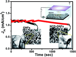
The improvement of the plasma illumination (PI) properties of a microplasma device due to the application of nanocrystalline diamond-decorated graphene nanoflakes (NCD-GNFs) as a cathode is investigated. The improved plasma illumination (PI) behavior is closely related to the enhanced field electron emission (FEE) properties of the NCD-GNFs. The NCD-GNFs possess better FEE characteristics with a low turn-on field of 9.36 V μm−1 to induce the field emission, a high FEE current density of 2.57 mA cm−2 and a large field enhancement factor of 2380. The plasma can be triggered at a low voltage of 380 V, attaining a large plasma current density of 3.8 mA cm−2 at an applied voltage of 570 V. In addition, the NCD-GNF cathode shows enhanced lifetime stability of more than 21 min at an applied voltage of 430 V without showing any sign of degradation, whereas the bare GNFs can last only 4 min. The superior FEE and PI properties of the NCD-GNFs are ascribed to the unique combination of diamond and graphene. Transmission electron microscopic studies reveal that the NCD-GNFs contain nano-sized diamond films evenly decorated on the GNFs. Nanographitic phases in the grain boundaries of the diamond grains form electron transport networks that lead to improvement in the FEE characteristics of the NCD-GNFs.


Introduction

Basically, microplasma-based devices symbolize a photonics technology at the connection of plasma science, optoelectronics, and materials science. Such plasma-based devices display pronounced prospective for a broad spectrum of applications in microdisplays, materials synthesis, elemental analysis and detection of environmentally hazardous or poisonous gases or vapors. In the operation of a microplasma device, the stability of the plasma is of great concern.1–3 Materials with a large secondary electron emission efficiency are thus commonly used as the cathode for these devices. However, the robustness (the lifetime) of the devices is a characteristic which is of even more importance in device applications. Diamond and graphene, being distinctive allotropes of carbon with unique physical and chemical characteristics, have attracted profound scientific and technological interest in recent years.4–7 Diamond, with a strong covalently bonded crystal structure and a high negative electron affinity (NEA) when H-terminated,8,9 is seen as a candidate for a potential field electron source exhibiting high lifetime and reliability. Additionally, diamond unveils a large secondary electron emission efficiency, which is particularly capable for serving as a cathode material in microplasma-based devices.10 Nevertheless, the large band gap (5.5 eV) in diamond considerably hampers the field electron emission (FEE) behavior because of the lack of free electrons necessary for field emission. High quality field electron emitters entail both a sufficient supply of electrons from back contact materials and effectual transport and efficient emission from the emitting sites.

Graphene is a two-dimensional honeycomb lattice consisting of hexagonally arrayed sp2-bonded carbon atoms.11 The open surface and sharp edge of graphene create a large aspect ratio thus making it an attractive candidate for FEE applications.12,13 Recent reports indicate the turn-on field for flat graphene sheets to be high.14 An alternative configuration is the use of graphene nanoflakes (GNFs) because of an abundant existence of sharp edge planes in GNFs, which can be a high density source of individual field emission sites. The presence of emissive sites in GNFs is particularly useful and relevant for high efficiency graphene-based field electron emitters.15 GNFs are made up of vertically stacked graphene sheets which are very much unlike carbon nanowalls associated with highly defective nanostructured graphite.16 However, the short lifetime and the poor stability of the graphene emitters, in a plasma environment, are major barriers preventing their beneficial integration. Based on the above, we are motivated to find that stable and reliable microplasma devices could be fabricated based on an effective combination of diamond and graphene. In order to fabricate such diamond-graphene hybrid devices, it is important to create diamond/graphene heterostructures. To date, there have only been limited reports regarding the growth of diamond on graphene layers.17–19 This is primarily due to issues associated with structural and interfacial integration of the materials and the resulting FEE characteristics, which leaves room for reliable improvement.

In this study, nanocrystalline diamond (NCD) grains were decorated on GNFs using a microwave plasma enhanced chemical vapor deposition (MWPECVD) process as a first step towards the fabrication of diamond-graphene hybrid FEE materials as a cathode for fabricating microplasma devices. Enhanced plasma illumination (PI) properties were observed. Noticeably, a better lifetime stability for the microplasma devices has been accomplished that is interrelated to the FEE behavior of the cathode materials. A promising mechanism for such a phenomenon is proposed.

Experimental methods

n-Type Si substrates were used to grow GNFs. Prior to growth, the substrates were pretreated with N2 plasma at 700 W at 40 mbar for 5 min, while the substrate temperature was maintained at 700–900 °C due to bombardment of species in the plasma. The synthesis of GNFs was carried out in a SEKI MWPECVD system, equipped with a 1.5 kW, 2.45 GHz microwave source using CH4/N2 (gas flow ratio = 3[thin space (1/6-em)]:[thin space (1/6-em)]2) plasma at 900 W for a duration of 5 min. The samples were allowed to cool under a constant N2 flow. The conditions used were similar to the ones used in our previous publication.20 The NCD films were then directly grown on the bare GNFs using an ASTeX 6500 series MWPECVD system in a CH4 (6%)/H2 (91%)/N2 (3%) plasma with a microwave power of 3000 W for 30 min. The pressure and the flow rate were maintained at 20 Torr and 300 sccm, respectively. The samples are hereafter referred to as NCD-GNFs.

The morphology and the crystalline quality of the samples were examined using scanning electron microscopy (SEM; FEI Quanta 200 FEG microscope) and confocal micro-Raman spectroscopy (Horiba Jobin-Yuan T64000 spectrometer; λ = 488 nm and spot size = ∼1 μm). The local microstructure and bonding structure of the samples were studied using TEM (JEOL 2100F) and electron energy loss spectroscopy (EELS) (Gatan Enfina), respectively. The FEE properties of the samples were measured in a parallel plate configuration, in which the anode was a Mo rod (2 mm in diameter) and the cathode was the NCD-GNFs. The cathode-to-anode separation was controlled by a micrometer. The FEE current density versus applied field (JeE) characteristics were acquired using a Keithley 2410 electrometer and these were elucidated using the Fowler–Nordheim (F–N) theory.21 The turn-on field (E0) is nominated as the intersection of the straight lines extrapolated from the high-field and low-field segments of the F–N plots, which are ln(Je/E2) versus 1/E plots.

To investigate the feasibility of using NCD-GNF materials as a cathode for a microplasma device, indium tin oxide (ITO)-coated glass was used as the anode and the NCD-GNFs were used as the cathode. The cathode-to-anode separation was fixed with a 1 mm polytetrafluroethylene spacer with a 3 mm diameter opening to form a microcavity. The schematic of the configuration is shown in Fig. 1. The microplasma device was placed in a glass chamber, which was evacuated to reach a base pressure of 0.1 mTorr and then purged with Ar for 10 min. Ar was channelled into the chamber at a flow rate of 10 sccm and the PI measurements were carried out at a pressure of 2 Torr. The plasma was triggered using a direct current voltage source, with a maximum applied voltage of 1000 V, and was connected to the device through a 500 kΩ resistor.


image file: c6ra07116c-f1.tif
Fig. 1 Schematic of the microplasma device measurement.

Results and discussion

Fig. 2a shows the SEM image of the bare GNFs that are flake-like structures consisting of randomly interwoven sharp edges with open spaces between them. The TEM analysis of bare GNFs (inset of Fig. 2a) confirms that the flakes are made up of a large number of graphene layers and graphitic edges. The vertically aligned orientation is a unique feature of the MWPECVD synthesis route and it provides an excellent structure for an electron emitter.15 The SEM image of Fig. 2b reveals that the NCD material decorates the GNFs with full coverage. The uniqueness in the method lies in obtaining NCD films in the absence of nucleation by seeding or any other pretreatments on the bare GNFs prior to the growth. It has been proposed that the nucleation of diamond started with the adherence of C–H bonds22 onto the GNFs, forming defect sites on the sp2 graphene network.23,24 The continued hydrogenation of the GNFs will either result in clustering of sp3 defects or it will increase the density of isolated sp3 point defects. The sp3 defects offer suitable sites for nucleation of carbon nanoparticles. Initially, an amorphous layer is formed,25 which then undergoes a phase transition into diamond nuclei.26
image file: c6ra07116c-f2.tif
Fig. 2 SEM micrographs for (a) bare GNFs, where the inset shows the corresponding TEM micrograph, and (b) NCD-GNFs.

Raman spectroscopy is one of the most powerful non-destructive techniques for characterization of carbon materials. The Raman spectrum of bare GNFs exhibits four major bands, denoted as D (1360 cm−1), G (1588 cm−1), G′ (1620 cm−1) (spectrum I of Fig. 3a) and 2D (2727 cm−1) (spectrum I of Fig. 3b).27–31 Spectrum II in Fig. 3a corresponding to the NCD-GNFs contains similar peaks to that of the GNFs (cf. spectrum I), i.e. it contains D, G and G′ bands and a 2D band with the exception of a ν3 peak at 1539 cm−1. Raman analysis of spectrum II of Fig. 3b shows that the 2D band exhibits a blue shift of 3 cm−1 compared to the bare GNFs (spectrum I of Fig. 3b), conceivably due to the bond angle disorder and compressive stress at the sp2:sp3 composite interface.32 The diamond peak at 1332 cm−1 is not clearly observed due to the nano-sized diamond grains. The existence of diamond in these materials will be revealed by TEM examinations.


image file: c6ra07116c-f3.tif
Fig. 3 (a and b) Confocal micro-Raman spectra for (I) bare GNFs and (II) NCD-GNFs.

The TEM image shown in Fig. 4a illustrates that the NCD films containing diamond grains about tens of nano-meters in size conformally cover the GNFs. The selective area electron diffraction (SAED) pattern of the NCD-GNFs is shown in the inset of Fig. 4a. Ring-shaped diffraction rings corresponding to the (111), (220) and (311) lattice planes of diamond are perceived, confirming that the nano-sized particles are NCD grains. There is a prominent diffused ring at the center of the SAED pattern, representing the presence of sp2-bonded carbon (amorphous or graphitic phase). Fig. 4b shows a high resolution TEM (HRTEM) structure image of the NCD-GNFs, corresponding to the designated region A in Fig. 4a. The NCD grains are ∼5 nm in size. The Fourier transformed diffractogram (ft0b) corresponding to the whole structure image in Fig. 4b shows a spotted diffraction pattern arranged in a ring (designated as d), which represents the randomly oriented diamond grains. The diffuse diffraction pattern located at the center of the ft0b image (designated as g) corresponds to the graphitic (g) phase. The ft1 image corresponding to large aggregates in region 1 and the ft2 image corresponding to region 2 show a spotted diffraction pattern arranged in a ring, which highlights the presence of the diamond (d) grains. Hence it is evident that the small clusters are nano-sized diamond grains, which are surrounded by nanographitic grain boundaries. In addition, the ft3 image corresponding to region 3 highlights the graphitic layers in the GNFs. The phase constituents in these NCD-GNF materials are better illustrated by a composed inverse FT image (Fig. 4c), which is the superposition of the inverse FT images corresponding to diamond and those corresponding to graphite diffraction spots (yellow and green circles in the inset FT pattern of Fig. 4c, respectively). In this figure, it is evident that the materials encasing the GNFs consist of nanodiamond grains, which are evenly distributed in nanographitic clusters.


image file: c6ra07116c-f4.tif
Fig. 4 (a) TEM micrograph for the NCD-GNFs with the inset showing the selective area electron diffraction (SAED) pattern, (b) HRTEM image of the NCD-GNFs of the designated region A in (a). The inset ft0b shows the Fourier transformed diffractogram corresponding to the entire structure images in (b), whereas the ft images corresponding to the regions marked 1–3 in the HRTEM image are shown in the insets ft1–ft3, respectively, to illustrate the presence of diamond, nanographite and graphene phases, (c) inverse Fourier transformed image corresponding to (b), and (d) core-loss and (e) plasmon-loss EELS spectra, where (I) is for bare GNFs and (II) is for NCD-GNFs.

EELS spectra were recorded in the carbon K-edge region of the NCD-GNFs to explicitly discriminate between the different carbon materials, for instance diamond, graphite and amorphous carbon (a-C).33 To facilitate the comparison, core-loss and plasmon-loss EELS spectra of the bare GNFs are also included (spectra I of Fig. 4d and e, respectively). The core-loss EELS spectrum of the bare GNFs contains a π* band near 284.5 eV and a band near 289 eV (spectrum I of Fig. 4d). In contrast, the core-loss EELS spectrum of the NCD-GNFs contains a sharp peak at 292 eV (σ* band) and a dip in the vicinity of 302 eV, which are the typical EELS signals of sp3-bonded carbon, besides a small hump, representing sp2-bonded carbon (285 eV, π* band) (spectrum II of Fig. 4d). In contrast, in Fig. 4e, the plasmon-loss EELS spectrum of the bare GNFs contains a broad peak near ωg ∼ 27 eV (spectrum I), which corresponds to the graphitic phase,34–37 whereas that of NCD-GNFs (spectrum II) contains a ωd1 peak near 23 eV and a shoulder ωd2 near 33 eV with a ωd1d2 ratio slightly larger than 1/√2, which implies that there exists a ωa-C peak near 22 eV corresponding to an (a-C) phase.34–37 These EELS characteristics are in concurrence with the TEM microstructural observations. Hence, it is evident from the TEM and EELS studies that the NCD films are conformally decorating the GNFs and each NCD grain is surrounded by nanographitic (or a-C) grain boundaries.

FEE measurements were carried out on the bare GNFs and the NCD-GNFs, and the results are shown in Fig. 5 with the inset showing the F–N plot. The NCD-GNFs possess slightly better FEE properties than the bare GNFs do. While the FEE process of the bare GNFs can be turned on at (E0)GNFs = 15.0 V μm−1, attaining a FEE current density of (Je)GNFs = 1.24 mA cm−2 at an applied field of 24.0 V μm−1 (curve I of Fig. 5), the decoration of NCD films on the GNFs markedly enhanced the FEE properties of the materials. The NCD-GNFs can be turned on at a smaller field, i.e. (E0)NCD-GNFs = 9.36 V μm−1, and exhibit a higher FEE current density of (Je)NCD-GNFs = 2.57 mA cm−2 at an applied field of 24.0 V μm−1 (curve II of Fig. 5). The field enhancement factor (β) corresponding to the bare GNFs and the NCD-GNFs was calculated from the slope of the F–N plots, which is shown as an inset in Fig. 5. The β factors were estimated to be (β)GNFs = 1560 and (β)NCD-GNFs = 2380 for the bare GNFs and NCD-GNFs, respectively. These FEE parameters are listed in Table 1. Therefore, the coating of NCD on GNFs does provide a benefit for the FEE emitters.


image file: c6ra07116c-f5.tif
Fig. 5 Field electron emission (FEE) current density (Je) as a function of applied field (E) of (I) bare GNFs and (II) NCD-GNFs emitters. The inset shows the corresponding Fowler–Nordheim plots, i.e. ln(Je/E2)–1/E plots.
Table 1 Field electron emission and plasma illumination properties of bare GNFs and NCD-GNFsa
Samples Field electron emission (FEE) Plasma illumination (PI)
E0 (V μm−1) Je (mA cm−2) @24.0 V μm−1 β Eb (V mm−1) JPI (mA cm−2) @570 V τPI (min) @430 V
a E0: the turn-on field for the FEE process that was designated as the interception of the lines extrapolated from the high-field and low-field segments of the F–N plots. Je: the FEE current density evaluated at the applied field designated. β: the field enhancement factor. Eb: the breakdown field for the PI process. JPI: the PI current density evaluated at an applied voltage of 500 V. τPI: the lifetime stability tested under an applied voltage of 430 V.
Bare GNFs 15.0 1.24 1560 400 3.3 4
NCD-GNFs 15.2 2.57 2380 380 3.8 23


The performance of the microplasma devices, with NCD-GNFs as the cathodes, was then investigated for using high FEE materials as a cathode for enhancing their PI behavior. Fig. 6 shows a series of photographs of the PI intensity of the microplasma devices, which utilized the bare GNFs (image series I of Fig. 6) and the NCD-GNFs (image series II of Fig. 6) as cathode materials. The intensity of the plasma increases monotonically with the applied voltage. The bare GNF-based microplasma devices need 400 V (breakdown field of Eb = 400 V mm−1) to trigger the plasma, while the NCD-GNF-based microplasma devices can be triggered by a voltage of 380 V (Eb = 380 V mm−1). The PI characteristics are better illustrated by the variation of the plasma current density (JPI) versus voltage, which is plotted in Fig. 7a. The bare GNF-based microplasma devices (curve I of Fig. 7a) show a JPI value of 3.3 mA cm−2 at an applied voltage of 570 V, whereas JPI achieves 3.8 mA cm−2 at the same applied voltage for the devices using the NCD-GNFs as the cathode (curve II of Fig. 7a). The PI characteristics of the bare GNFs and NCD-GNFs are also listed in Table 1. What is intriguing is that the NCD-GNF-based microplasma devices not only show a better PI behavior than that of the bare GNF cathode-based microplasma devices, but they also exhibit superior robustness, compared with the bare GNF-based ones. To evaluate the stability of the GNF and the NCD-GNF cathode microplasma devices, JPI was monitored over a long period with a constant applied voltage of 430 V (Fig. 7b), where the bare GNF-based microplasma devices exhibit 0.8 mA cm−2 and the NCD-GNF-based microplasma devices exhibit 1.3 mA cm−2 plasma current density. The JPI value of the bare GNF-based microplasma devices decayed very fast. It occurred after 4 min (240 s) of plasma ignition (curve I of Fig. 7b). The GNFs are completely damaged after lifetime measurements (inset I of Fig. 7b). Interestingly, for the NCD-GNF-based devices, the plasma current is upheld for a period over 23 min (1380 s) (curve II of Fig. 7b). The NCD-GNFs can survive even after 23 min of plasma discharge (inset II of Fig. 7b), illustrating the higher robustness of these devices.


image file: c6ra07116c-f6.tif
Fig. 6 Photographs of plasma illumination (PI) characteristics of microplasma devices using (I) bare GNFs and (II) NCD-GNFs as the cathode.

image file: c6ra07116c-f7.tif
Fig. 7 (a) Plasma current density (JPI) versus applied voltage and (b) plasma lifetime measurements of a microplasma device, which utilized ITO-coated glass as the anode and either (I) bare GNFs or (II) NCD-GNFs as cathode materials, at an applied voltage of 430 V. The insets show the SEM micrographs of (I) the GNF and (II) the NCD-GNF cathode materials used in the microplasma devices after the plasma discharge.

It should be noted that the electric field required to trigger the Ar plasma (380–400 V mm−1) is much smaller than E0 for inducing the FEE process (i.e. 15.0–15.2 V μm−1) for both the GNFs and the NCD-GNFs. It is not straightforward to understand how the better FEE properties of the NCD-GNF materials can enhance the PI behavior of the corresponding microplasma devices. Usually, the Ar plasma can be triggered whenever electrons emitted from the cathodes reach a kinetic energy larger than the ionization energy of the Ar species (14.7 eV). After the initiation of the Ar plasma, the NCD-GNF (or GNF) cathode materials mainly serve as a good source of secondary electrons for maintaining the ignition of the plasma. The better FEE properties of the NCD-GNFs compared to those of the GNFs seem to show an insignificant superiority in maintaining the plasma in the microplasma devices. However, when the plasma in the devices was ignited, a sheath is formed in the vicinity of the cathode, which is of the order of tens of microns.38 The applied voltage will be fully exerted at the sheath. The electric field experienced by the cathode will increase abruptly to around 40 V μm−1, which is markedly larger than the E0 value for turning on the FEE process of the cathode materials. Therefore, the superior FEE properties for the cathode materials might provide a larger FEE current density for the microplasma devices. Apparently, both the superior FEE properties and higher secondary electron emission efficiency for the NCD-GNFs contribute to the better PI performance of the microplasma devices, which are based on the NCD-GNFs as the cathode, as compared to the bare GNF-based ones.

Now the question that arises is how does the microstructure support the electron transport mechanism of the NCD-GNFs for obtaining these enhanced FEE and PI properties? It is observed from TEM studies (cf. Fig. 4) that GNFs are decorated by NCD films and each diamond grain in the NCD films is surrounded by nanographitic grain boundaries. Based on the TEM observations, the mechanism for the improved FEE behavior of the NCD-GNFs can be explained as follows: first, the good electron transport properties of the GNFs supplies sufficient electrons to the NCD region. The nanographitic phases present in the grain boundaries of the NCD grains provide efficient transport paths for the electrons to reach the surface of the NCD grains, which served as the emitting surface. Then the electrons are emitted to a vacuum without any difficulty as the diamond H-terminated surface has a NEA.5,6 Additionally, the vertically aligned structure of the GNFs facing the anode can be considered as an additional reason for improving the FEE and PI properties of the NCD-GNFs.

Conclusions

A facile and reproducible way of decorating GNFs with NCD materials results in superior functioning and improved lifetimes of microplasma devices compared to bare GNFs as cathodes. Detailed structural characterizations through TEM reveal that the GNFs are homogeneously covered with NCD grains possessing nanographitic grain boundaries. As a result, the microplasma devices based on the NCD-GNF cathodes show better PI characteristics due to enhanced FEE properties of the cathode materials. More importantly, a JPI of 1.31 mA cm−2 (a constant applied voltage of 430 V) is maintained for a period over 23 min, displaying the better plasma lifetime stability for the NCD-GNF-based microplasma devices, as compared to that of the bare GNFs (plasma lifetime stability of 4 min). These results point to the possibility of using NCD-GNFs as potential candidates for applications in microplasma devices.

Acknowledgements

The authors would like to thank the financial support of the Research Foundation Flanders (FWO) via Research Project G.0456.12 and G0044.12N and the Methusalem “NANO” network. Kamatchi Jothiramalingam Sankaran and Paulius Pobedinskas are Postdoctoral Fellows of the Research Foundation-Flanders (FWO). SK Bikkarolla acknowledges support from Ulster University through the Vice-Chancellor's Research Scholarship (VCRS) award.

References

  1. L. G. Meng, C. L. Liu, H. F. Liang and Z. H. Liang, Phys. Lett. A, 2008, 372, 6504 CrossRef CAS.
  2. Z. S. Yang, H. Shirai, T. Kobayashi and Y. Hasegawa, Thin Solid Films, 2007, 515, 4153 CrossRef CAS.
  3. S. Kanazawa, R. Daidai, S. Akamine and T. Ohkubo, Surf. Coat. Technol., 2008, 202, 5275 CrossRef CAS.
  4. Y. W. Cheng, C. K. Lin, Y. C. Chu, A. Abouimrane, Z. Chen, Y. Ren, C. P. Liu, Y. Tzeng and O. Auciello, Adv. Mater., 2014, 26, 3724 CrossRef CAS PubMed.
  5. R. Caterino, R. Csiki, A. Lyuleeva, J. Pfisterer, M. Wiesinger, S. D. Janssens, K. Haenen, A. Cattani-Scholz, M. Stutzmann and J. A. Garrido, ACS Appl. Mater. Interfaces, 2015, 7, 8099 CAS.
  6. R. J. Nemanich, J. A. Carlisle, A. Hirata and K. Haenen, MRS Bull., 2014, 39, 490 CrossRef CAS.
  7. L. Liu, Z. Niu, L. Zhang, W. Zhou, X. Chen and S. Xie, Adv. Mater., 2014, 26, 4855 CrossRef CAS PubMed.
  8. H. Yamaguchi, T. Masuzawa, S. Nozue, Y. Kudo, I. Saito, J. Koe, M. Kudo, T. Yamada, Y. Takakuwa and K. Okano, Phys. Rev. B: Condens. Matter Mater. Phys., 2009, 80, 165321 CrossRef.
  9. M. W. Geis, S. Deneault, K. E. Krohn, M. Marchant, T. M. Lyszczarz and D. L. Cooke, Appl. Phys. Lett., 2005, 87, 192115 CrossRef.
  10. S. Kunuku, K. J. Sankaran, C. L. Dong, N. H. Tai, K. C. Leou and I. N. Lin, RSC Adv., 2014, 4, 47865 RSC.
  11. A. K. Geim and K. S. Novoselov, Nat. Mater., 2007, 6, 183 CrossRef CAS PubMed.
  12. Z. S. Wu, S. Pei, W. Ren, D. Tang, L. Gao, B. Liu, F. Li, C. Liu and H. M. Cheng, Adv. Mater., 2009, 21, 1756 CrossRef CAS.
  13. U. A. Palnitkar, R. V. Kashid, M. A. More, D. S. Joag, L. S. Panchakarla and C. N. R. Rao, Appl. Phys. Lett., 2010, 97, 063102 CrossRef.
  14. S. Santandrea, F. Giubileo, V. Grossi, S. Santucci, M. Passacantando, T. Schroeder, G. Lupina and A. Di Bartolomeo, Appl. Phys. Lett., 2011, 98, 163109 CrossRef.
  15. N. Soin, S. S. Roy, S. Roy, K. S. Hazra, D. S. Misra, T. H. Lim, C. J. Hetherington and J. A. McLaughlin, J. Phys. Chem. C, 2011, 115, 5366 CAS.
  16. A. T. H. Chuang, J. Robertson, B. O. Boskovic and K. K. K. Koziol, Appl. Phys. Lett., 2007, 90, 123107 CrossRef.
  17. Y. Wang, M. Jaiswal, M. Lin, S. Saha, B. Ozyilmaz and K. P. Loh, ACS Nano, 2012, 6, 1018 CrossRef CAS PubMed.
  18. Y. Tzeng, W. L. Chen, C. Wu, J. Y. Lo and C. Y. Li, Carbon, 2013, 53, 120 CrossRef CAS.
  19. D. Varshney, C. Rao, M. Guinel, Y. Ishikawa, B. Weiner and G. Morell, J. Appl. Phys., 2011, 110, 044324 CrossRef.
  20. N. Soin, S. S. Roy, C. O’Kane, T. H. Lim, C. J. D. Hetherington and J. A. McLaughlin, CrystEngComm, 2011, 13, 312 RSC.
  21. R. H. Fowler and L. Nordheim, Proc. R. Soc. London, Ser. A, 1928, 119, 173 CrossRef CAS.
  22. K. J. Sankaran, N. Kumar, J. Kurian, R. Ramadoss, H. C. Chen, S. Dash, A. K. Tyagi, C. Y. Lee, N. H. Tai and I. N. Lin, ACS Appl. Mater. Interfaces, 2013, 5, 3614 CAS.
  23. J. O. Sofo, A. S. Chaudhari and G. D. Barber, Phys. Rev. B: Condens. Matter Mater. Phys., 2007, 75, 153401 CrossRef.
  24. D. C. Elias, R. R. Nair, T. M. G. Mohiuddin, S. V. Morozov, P. Blake, M. P. Halsall, A. C. Ferrari, D. W. Boukhvalov, M. I. Katsnelson, A. K. Geim and K. S. Novoselov, Science, 2009, 323, 610 CrossRef CAS PubMed.
  25. L. T. Sun, J. L. Gong, Z. Y. Zhu, D. Z. Zhu, S. X. He, Z. X. Wang, Y. Chen and G. Hu, Appl. Phys. Lett., 2004, 84, 2901 CrossRef CAS.
  26. M. G. Fyta, I. N. Remediakis and P. C. Kelires, Phys. Rev. B: Condens. Matter Mater. Phys., 2003, 67, 035423 CrossRef.
  27. A. C. Ferrari and J. Robertson, Phys. Rev. B: Condens. Matter Mater. Phys., 2000, 61, 14095 CrossRef CAS.
  28. F. Tuinstra and J. L. Koenig, J. Chem. Phys., 1970, 53, 1126 CrossRef CAS.
  29. A. C. Ferrari and J. Robertson, Phys. Rev. B: Condens. Matter Mater. Phys., 2001, 64, 075414 CrossRef.
  30. J. Kastner, T. Pichler, H. Kuzmany, S. Curran, W. Blau, D. N. Weldon, M. Delamesiere, S. Draper and H. Zandbergen, Chem. Phys. Lett., 1994, 221, 53 CrossRef CAS.
  31. C. Casiraghi, A. Hartschuh, H. Qian, S. Piscanec, C. Georgi, A. Fasoli, K. S. Novoselov, D. M. Basko and A. C. Ferrari, Nano Lett., 2009, 9, 1433 CrossRef CAS PubMed.
  32. R. F. Egerton, Electron Energy Loss Spectroscopy in the Electron Microscope, Plenum, New York, 2nd edn, 1996 Search PubMed.
  33. A. Dato, V. Radmilovic, Z. Lee, J. Philips and M. Frenklach, Nano Lett., 2008, 8, 2012 CrossRef CAS PubMed.
  34. D. M. Gruen, S. Liu, A. R. Krauss, J. Luo and X. Pan, Appl. Phys. Lett., 1994, 64, 1502 CrossRef CAS.
  35. P. Kovarik, E. B. D. Bourdon and R. H. Prince, Phys. Rev. B: Condens. Matter Mater. Phys., 1993, 48, 12123 CrossRef CAS.
  36. M. H. Gass, U. Bangert, A. L. Bleloch, P. Wang, R. R. Nair and A. K. Geim, Nat. Nanotechnol., 2008, 3, 676 CrossRef CAS PubMed.
  37. A. V. Generalov and Y. S. Dedkov, Carbon, 2012, 50, 183 CrossRef CAS.
  38. M. A. Lieberman and A. J. Lichtenberg, Principles of plasma discharges and materials processing, John Wiley & Sons, Hoboken, NJ, 2nd edn, 2005 Search PubMed.

This journal is © The Royal Society of Chemistry 2016
Click here to see how this site uses Cookies. View our privacy policy here.