Ligang Xua,
Yunjie Daia,
Hongmei Zhang*a and
Wei Huang*ab
aKey Laboratory for Organic Electronics and Information Displays (KLOEID), Institute of Advanced Materials (IAM), Jiangsu National Synergetic Innovation Center for Advanced Materials (SICAM), Nanjing University of Posts & Telecommunications, 9 Wenyuan Road, Nanjing 210023, China. E-mail: iamhmzhang@njupt.edu.cn; iamwhuang@njupt.edu.cn; Tel: +86 25 85866396 Tel: +86 25 85866533
bKey Laboratory of Flexible Electronics (KLOFE), Institute of Advanced Materials (IAM), Jiangsu National Synergetic Innovation Center for Advanced Materials (SICAM), Nanjing Tech University (NanjingTech), 30 South Puzhu Road, Nanjing 211816, China
First published on 11th May 2016
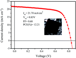
In this paper, we report the fabrication of high crystalline perovskite film planar-heterojunction solar cells by a facile one-step spin-coating technique with improved control of thermal annealing time and solution concentration. We used an indium-doped tin oxide glass/poly(3,4-ethylenedioxythiophene):poly(styrene-sulfonate) (PEDOT:PSS) substrate as the hole transport layer, a PHJ of CH3NH3PbI3 perovskite fabricated by one-step spin-coating processing as the active layer and fullerene structure as the electron transport layer, a thin bathocuproine (BCP) film as an hole-blocking layer (HBL), and an aluminum (Al) layer as the negative electrode. The optimized device under AM 1.5 (100 mW cm−2) radiation achieved a high efficiency of 12.21% with an open circuit voltage of 0.83 V and FF of 0.68. Meanwhile, the devices do not show obvious hysteresis photovoltaic response, which has been a fundamental bottleneck for perovskite devices. The effects of MAI concentration and annealing time on the solar cells were also discussed on the basis of experimental observations.
Spin-coating, one of the cheapest film production methods, is widely used in solution-processed planar heterojunction perovskite solar cells. However, films produced by the conventional spin-coating methods were found to be composed of large CH3NH3PbI3 grains and many uncovered pin-hole areas, which could produce the shunting in such planar heterojunction devices.26 Therefore, a nonporous homogenous perovskite film must be fabricated to obtain an excellent performance of planar device. To date, the CH3NH3PbI3 layer in the most efficient planar solar cells has been fabricated by either vapor deposition, a two-step sequential solution deposition, or a vapor-assisted two-step reaction process.26–28 The vapor deposition process is likely to increase the manufacturing cost.26 Moreover, the sequential two-step deposition on planar substrates has two problems: one is the incomplete conversion of PbI2 and the other is the uncontrolled perovskite crystal sizes as well as surface morphology.26,29 Therefore, a facile one-step spin-coating technique that can produce high-quality films with controlled morphology is highly desirable for the construction of planar devices. Seok et al.13 reported the solution-process fabrication of efficient perovskite solar cells comprised of bilayer architecture and MAPb(I1−xBrx)3 perovskites on the mesoporous TiO2 scaffold, with a 16.2% power-conversion efficiency (PCE) achieved under 1 sun illumination. Cheng et al.30 also reported a one-step, solvent-induced, fast crystallization-deposition method that results in flat, highly uniform CH3NH3PbI3 thin films. Inspired by their work and our previous works,25,31 highly efficient perovskite/fullerene planar-heterojunction solar cells were attempted to be fabricated by a facile one-step spin-coating technique.
Herein, we report the fabrication of ordered perovskite films planar-heterojunction solar cells by a facile one-step spin-coating technique. We used an indium-doped tin oxide glass (ITO)/poly(3,4-ethylenedioxythiophene):poly(styrene-sulfonate) (PEDOT:PSS) substrate as hole transport layer, a PHJ of CH3NH3PbI3 perovskite fabricated by one-step spin-coating processing as the active layer and fullerene structure as electron transport layer, a thin bathocuproine (BCP) film as an hole-blocking layer (HBL) and an aluminum (Al) layer as negative electrode. The optimized device under AM 1.5 (100 mW cm−2) radiation achieved a high efficiency of 12.21% with an open circuit voltage of 0.83 V and FF of 0.68. Meanwhile, the devices do not show obvious hysteresis photovoltaic response, which has been a fundamental bottleneck for perovskite devices.
:
3 v/v) at 60 °C for 12 h. The resulting solution was coated onto the PEDOT:PSS substrates by a one-step spin-coating process. During the spin-coating step, the substrate (around 1.5 cm × 1.5 cm) was treated with toluene drop-casting. A detailed time-rotation profile for the spin-coating is shown in ESI Fig. S1.† The film becomes darker after annealing at 100 °C for 5 min. The C60 (30 nm), BCP (10 nm) and Al (120 nm) were thermally deposited on the substrate inside a vacuum chamber. The evaporation rates were monitored by a quartz oscillator system, and the film thickness was calibrated by a surface profiler (Veeco Dektak 6M). Finally, the devices with an active area of 0.11 cm2 were strictly encapsulated with UV-curable epoxy before being taken out from the glove box.
The CH3NH3I (MAI) and PbI2 for MAPbI3 solution were stirred in a mixture of GBL and DMSO (7
:
3 v/v) as precursor solutions at varied concentrations. The resulting solution was coated onto the PEDOT:PSS substrates by a one-step spin-coating process. The film becomes darker after annealing at 100 °C for varied durations.
Fig. 1b shows the energy level of each layer in the device. The lowest unoccupied molecular orbital (LUMO) and the highest occupied molecular orbital (HOMO) levels of MAPbI3 perovskite are −3.9 and −5.4 eV, respectively, and those of C60 are −4.5 and −6.2 eV.32,33 C60 with a LUMO of −4.5 eV could be an electron acceptor for MAPbI3 perovskite to create a donor–acceptor PHJ system. Under irradiation, excitons are generated by the absorption of light in the perovskite layer. The oppositely charged holes and electrons in excitons are then separated at the donor–acceptor interface, and are transported by perovskite and C60, respectively, resulting in the photovoltaic effect.
The surface morphologies of the MAPbI3 perovskite films were examined by SEM, and the results are shown in Fig. 2. In Fig. 2a, we can see that the thin film is in fact very smooth and dense with some cracks in the surface. In Fig. 2b, the magnified SEM picture, we can observe that the surface exhibits a dense-grained uniform morphology with grain sizes in the range of 60–400 nm (Fig. 2c). The entire film is composed of a homogenous, well-crystallized perovskite layer (Fig. 4), which also enables the devices to show high efficiency and easy reproducibility.
Fig. 3 shows typical absorption spectra of a MAPbI3 film before and after 5 min annealing at the temperature of 100 °C. The absorption at wavelength of around 740 nm from the thin film increased during the 5 min of thermal annealing. And the perovskite film after annealing has an absorption profile that extends to NIR (800 nm) with a higher absorption at 550 nm, which indicates that after annealing the perovskite film is denser.16,19
![]() | ||
| Fig. 3 UV/Vis absorption spectra of PEDOT:PSS/perovskite films before and after annealing at 100 °C for 5 min. The inset shows the perovskite thin film after 5 min of annealing. | ||
The crystalline structure of MAPbI3 perovskite film before and after annealing on the glass/PEDOT:PSS substrate was characterized by X-ray diffraction and shown in the Fig. 4. It could be pointed out that the XRD pattern of lead iodide disappeared after spin-coating without annealing. The annealing step is just a crystal growth process which improves the crystal quality of perovskites as the relative intensity of perovskite XRD peaks increases, which also made the power conversion efficiency increase after thermal treatment (Table 1).
![]() | ||
| Fig. 4 XRD patterns of CH3NH3PbI3 film before and after annealing 100 °C for 5 min (MAIPbI3: 1.0 M MAI and 1.0 M PbI2). | ||
| MAI conc. (M) | Annealing time (min) | Jsc (mA cm−2) | Voc (V) | FF | PCE (%) |
|---|---|---|---|---|---|
| 0.8 | 5 | 20.80 | 0.86 | 0.56 | 10.03 |
| 1.0 | 5 | 21.70 | 0.83 | 0.68 | 12.21 |
| 1.2 | 5 | 22.10 | 0.77 | 0.64 | 10.94 |
| 1.0 | 0 | 0.92 | 0.70 | 0.15 | 0.09 |
| 1.0 | 3 | 19.76 | 0.82 | 0.66 | 11.13 |
| 1.0 | 10 | 19.33 | 0.77 | 0.64 | 9.46 |
| 1.0 | 15 | 14.50 | 0.78 | 0.30 | 3.37 |
The devices have a structure of ITO/PEDOT:PSS/MAPbI3/C60 (30 nm)/BCP (10 nm)/Al (120 nm). The device performance is very sensitive to thermal annealing time, MAI or PbI2 concentrations. Fig. 5a presents the current density–voltage (J–V) curves of the devices based on perovskite films prepared with varying MAI concentrations from 0.8 M to 1.2 M, demonstrating how the device performance was optimized. The photovoltaic parameters of devices are summarized in Table 1. A perovskite film prepared by higher MAI concentrations could increase the thickness of film. A thicker perovskite film absorbs more light and thus yields a larger photocurrent, while a thicker film causes loss of photovoltage, which might be due to the increased charge recombination. The highest PCE devices were obtained by annealing of MAPbI3 prepared by 1.0 M MAI at 100 °C for 5 min. The device was measured under AM 1.5 simulated one sun illumination. The best performing device has a Jsc of 21.7 mA cm−2, a FF of 0.68, an open circuit voltage (Voc) of 0.83 V and a PCE of 12.21%.
From the previous report,18 the morphology of a perovskite film can be controlled by annealing time, which has a great impact on the performance of the PHJ perovskite solar cells. Fig. 5b and Table 1 present the current density–voltage (J–V) curves of the devices based on perovskite films annealing of different periods. The highest PCE devices were obtained by annealing of MAPbI3 films at 100 °C for 5 min. Perovskite film coverage is large with a number of small pores after spin-coating. The small pores either increase in size or close up until the final crystalline phase is reached after different periods of the annealing process.18 The planar thin-film architecture's lower performance after annealing more than 5 min may arise from pin-hole formation, incomplete coverage of the perovskite resulting in low-resistance shunting paths and lost light absorption in the solar.26 Fig. 5c shows the incident photon to electron conversion efficiency (IPCE) spectrum of one optimized device, which indicates that the device shows a spectral response in the region from the visible to near infrared (400–800 nm) with a peak IPCE of over 90% at approximately 550 nm. The integrated Jsc of 21 mA cm−2 from the IPCE agree well with measured.
It is known that some perovskite solar cells show photocurrent hysteresis at scan direction and certain voltage scanning rate (or sweep delay time).34 The origin of photo current hysteresis was ascribed to either the traps, ferroelectric properties of the perovskite material and/or the electromigration of ions in the perovskites. Here we change the scanning rate from very fast to very slow, with a delay between measurement voltage points increasing from 0 to 500 ms. The J–V curves and the results measured by different sweep times and two opposite scan directions are shown in Fig. 6. Our device does not show obvious photocurrent hysteresis of photocurrent by changing the sweep rates or the directions in our devices. The main cause of hysteretic behavior in perovskite solar cells can be found in the formation of an internal field upon ion migration, and the role of the electron transport layer is of paramount importance in determining the device response to such a transient phenomenon.35 The C60 used as electron transport layer in our devices might improve charge extraction with respect to interfaces involving compact TiO2 and make the short-circuit current density insensitive to the transient phenomena to ions migration.
![]() | ||
| Fig. 6 Photocurrents of a high performance perovskite device measured with different delays between measurement points (a) and different sweep directions (b). | ||
The time-resolved photoluminescent (PL) decay curve of planar-heterojunction solar cell was also measured as shown in Fig. S2.† It can be seen that the photoluminescent (PL) decay curve was shorter than perovskite solar cell used TiO2 as electron transport layer from previous report,36 which confirmed the faster transfer of the charge carriers in our device. So our device might inject the charge carriers from MAPbI3 perovskite into C60 more efficiently than that from MAPbI3 perovskite into TiO2.
Footnote |
| † Electronic supplementary information (ESI) available. See DOI: 10.1039/c6ra07068j |
| This journal is © The Royal Society of Chemistry 2016 |