DOI:
10.1039/C6RA06688G
(Paper)
RSC Adv., 2016,
6, 59565-59573
Effects of spark plasma sintering conditions on the anisotropic thermoelectric properties of bismuth antimony telluride†
Received
14th March 2016
, Accepted 9th June 2016
First published on 10th June 2016
Abstract
Bismuth antimony telluride (BixSb2−xTe3, 0.4 < x< 0.6) is one of the best and most-used p-type semiconductor materials for near-room-temperature thermoelectric power generation. In this work, p-type Bi0.4Sb1.6Te3 samples were prepared under various conditions (temperature, holding time, and ramp-rate) using spark plasma sintering (SPS). The effects of SPS conditions on the anisotropic thermoelectric properties and microstructure evolutions were systematically investigated. The change of sintering temperature showed stronger influence than other sintering parameters to the resulting thermoelectric properties. Samples sintered over the temperature range between 653 K and 773 K showed significant differences in the degrees of orientations. The change was mainly caused by grain growth and re-orientation. Despite of the anisotropy, zT value as high as 1.2 to 1.3 was achieved over the temperature range of 300 to 360 K by directly using commercial power sintered at 723 and 773 K. The sintering profiles and microstructure evolutions during SPS were illustrated and the thermoelectric properties as a function of the degrees of orientations were shown and discussed in detail.
Introduction
Thermoelectrics is a promising alternative technology for energy conversion. It converts heat directly into electricity without any moving parts.1–3 This unique feature allows it to be utilized in applications like radioisotope generators in deep space probes, waste heat recovery in chimneys, etc. where maintenance needs to be avoided.4,5 The overall performance of a thermoelectric (TE) material is governed by a dimensionless figure-of-merit zT, which is expressed as zT = S2σT/κ, where T is temperature, S is Seebeck coefficient, σ is electrical conductivity, and κ is thermal conductivity, all of which are temperature dependent.6 A TE material is usually considered as commercially relevant when its average zT is close to or above one over its working temperature range.1
Bismuth antimony telluride (BixSb2−xTe3, 0.4 < x< 0.6) is one of the most commonly used p-type TE materials near room temperature. It has been frequently reported to have a zT higher than one at room temperature.7–11 In 2008, Ren's group successfully made nanostructured bismuth antimony tellurium alloys prepared by SPS, and a peak zT of 1.3 in the temperature range of 348 and 373 K was achieved.9 Later, Xie et al. prepared Bi–Sb–Te samples with nano-domains and coherent boundaries using melt spinning technique together with SPS resulting in a significant improvement of zT to a value of 1.5 at 390 K.7 In 2015, Kim et al. introduced dense dislocation arrays embedded in grain boundaries which effectively reduced the lattice thermal conductivity and an enhancement of zT up to 1.86 at 320 K was achieved.11
Bismuth antimony telluride is a typical TE material with anisotropic TE properties due to its crystal structure, which are sensitive to the characterization directions due to either anisotropic crystal structures or anisotropic grains. The electric conductivity, Seebeck coefficient, and thermal conductivity must be therefore measured in the same direction so the figure-of-merit zT is calculated in a proper way.12–17 For bismuth antimony telluride, its anisotropy is originated from the intrinsic misfit layered crystal structures of the material.18,19 Nevertheless, the change of anisotropy of the bulk samples can also be affected by the processing route as well.16
Fabricating TE materials using spark plasma sintering (SPS) is being increasingly used because SPS provide rapidly densified samples avoiding severe grain growth.20 Under the uniaxial pressure, the samples prepared by SPS are very likely to have orientations of the grains.21 For bismuth antimony telluride, textures were often observed for samples prepared by SPS.20,22,23 Böttner et al. from IPM Germany investigated the influence of the SPS sintering on the structural and mechanical properties of bismuth telluride-based materials.24 However, little attention was paid so far on the effect of SPS process conditions on the grain orientations and their correlation with the TE properties. Here, we conducted systematic experiments to investigate the influence of spark plasma sintering conditions on the microstructure and TE properties of bismuth antimony telluride. The grain texture was investigated by directionally characterizations of structural and TE characterizations. The figure-of-merit zT was properly calculated using the values measured in the same direction. The microstructure evolution and TE properties with respect to the sintering temperature, holding time, pressure, and ramp-rate were also discussed in detail.
Experimental
The starting material was commercial Bi0.4Sb1.6Te3 powder with a purity of >99% from the Sichuan Xinlong Tellurium Industry & Technique Development Co., Ltd. The particle size and morphology of the powder are given in Fig. S1 (see ESI†). For each sample preparation, 8 g of commercial powder was put into 1.27 cm in diameter of graphite die and sintered by spark plasma sintering (SPS) (Syntex Inc., Japan), with a pulsed direct current regulated by on![[thin space (1/6-em)]](https://www.rsc.org/images/entities/char_2009.gif) :off settings, each pulse lasts 3.3 ms and has a 12:2 on:off ratio. The experimental parameters such as sample temperature, electrical current between electrodes, pressure, and z-axis displacement (graphite punch movements along the pressure axis due to sample shrinkage) were all recorded simultaneously during the process. The pressure was applied before the current started and released gradually when the current stopped. An overview of the sintering conditions of the samples is shown in Table 1. Four variables, peak sintering temperature, holding time, uniaxial pressure, and ramp-rate, were investigated using 4 groups of samples.
:off settings, each pulse lasts 3.3 ms and has a 12:2 on:off ratio. The experimental parameters such as sample temperature, electrical current between electrodes, pressure, and z-axis displacement (graphite punch movements along the pressure axis due to sample shrinkage) were all recorded simultaneously during the process. The pressure was applied before the current started and released gradually when the current stopped. An overview of the sintering conditions of the samples is shown in Table 1. Four variables, peak sintering temperature, holding time, uniaxial pressure, and ramp-rate, were investigated using 4 groups of samples.
Table 1 Samples and their corresponding sintering parameters during SPS
| Sample # |
Variables |
Peak temperatureaT/K |
Holding timebt/min |
Uniaxial pressure P/MPa |
Ramp-ratecR/K min−1 |
|
Highest temperature during sintering.
Holding time at peak temperature.
Ramp-rate during heating up.
|
| 1 (ST-653) |
Peak temperature |
653 |
0 |
50 |
50 |
| 2 (ST-683) |
683 |
0 |
50 |
50 |
| 3 (ST-723) |
723 |
0 |
50 |
50 |
| 4 (ST-773) |
773 |
0 |
50 |
50 |
| 3 |
Holding time |
723 |
0 |
50 |
50 |
| 5 |
723 |
5 |
50 |
50 |
| 6 |
723 |
10 |
50 |
50 |
| 7 |
Uniaxial pressure |
723 |
5 |
30 |
50 |
| 3 |
723 |
5 |
50 |
50 |
| 8 |
Ramp-rate |
723 |
5 |
50 |
30 |
| 3 |
723 |
5 |
50 |
50 |
| 9 |
723 |
5 |
50 |
300 |
After SPS, the disc-shaped samples with a thickness of ∼1 cm and diameter of 12.5 cm were cut into rectangular (3 × 3 × 10 mm3) and square shapes (6 × 6 × 1 mm3), along the parallel (║p) and perpendicular (⊥p) direction of the pressure. These samples were used for measuring the electrical conductivity (σ), Seebeck coefficient (S), carrier mobility (μ), and thermal conductivity (κ) along the same direction and subsequently the determination of zT, as shown in Fig. S4 (see ESI†). The electrical conductivity and Seebeck coefficient were measured simultaneously using an ULVAC-RIKO ZEM-3 from room temperature up to 473 K under 0.1 bar of helium. Hall measurement was also carried out at room temperature by van-der-Pauw method with a variable magnet field to determine the carrier density and resistivity. The thermal conductivity (κ) was determined from the thermal diffusivity (α), the mass density (D) and the specific heat capacity (Cp) according to the equation κ = αDCp. The thermal diffusivity was obtained by the laser flash method (Netzsch LFA-457, Germany), the mass densities of the samples were measured by Archimedes' method using water with surfactant, and the specific heat capacity was measured using a differential scanning calorimeter (Netzsch DSC 404C, Germany). X-ray diffraction (XRD) pattern was obtained using a Bruker D8 diffractometer (Bruker, Germany) with Cu-Kα radiation. A scanning electron microscope (SEM, Supra; Carl Zeiss, Inc., Germany) with energy-dispersive X-ray spectroscopy (EDS) and electron backscatter diffraction (EBSD) was used to study the microstructures, chemical compositions, and texture of the samples. EBSD mapping was performed on fine polished sample surface with a step sized of 3 μm and with index material data file from literature.25
Results and discussion
Influence of peak sintering temperature
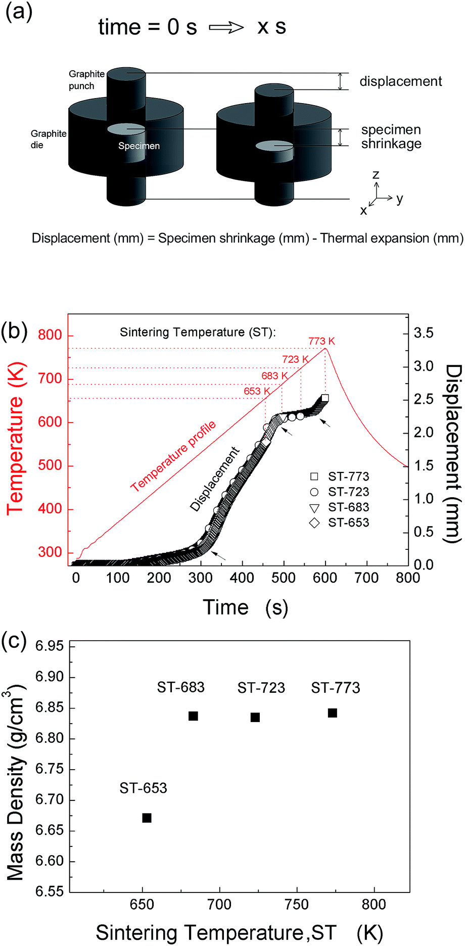
Analyzing the sintering profiles of the SPS is an important tool to understand how the sintering process occurs. Fig. 1a shows the sample displacement, which takes into an account the thermal expansion of graphite punches. Fig. 1b shows the displacement versus time of the sintering profiles from 4 different specimens sintered with peak temperatures of 653, 683, 723, and 773 K. The displacement curve for ST-773 sample has multiple turnings at 330, 480, and 580 s. The 3 turning points are pointed out by arrows in Fig. 1b. The first turning started at 330 s (@550 K) as the first displacement took place, indicating the softening and compression of the powder precursors. The second turning happened at 480 s (@670 K) after the rapid displacement slowed down, and then the third turning happened at 580 s (@750 K). On the other hand, the mass density of the samples increased with increasing sintering temperature and reached a saturation level at 683 K, as shown in Fig. 1c. Therefore, the second turning represents the point close to the highest relative density, and the third turning was caused by other mechanisms, e.g. melting and squeezing out of compounds, and will be discussed in the following. The other three samples have showed very similar sintering profiles, which indicated a very good reproducibility during SPS.
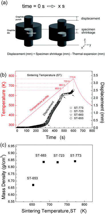 |
| | Fig. 1 (a) Schematics illustration/explanation of displacement for a specimen inside graphite die during SPS. (b) Sintering profile for 4 specimens sintered with peak temperatures (ST) of 653 K, 683 K, 723 K, and 773 K, which are denoted as ST-653, ST-683, ST-723, and ST-773, respectively. (c) Mass density of the sintered samples. | |
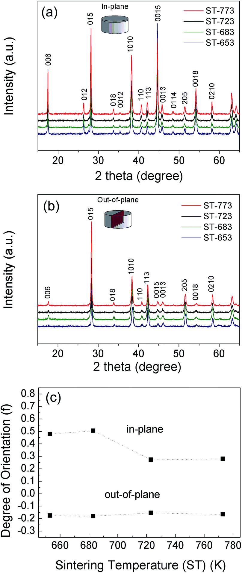
X-ray diffraction patterns of the specimens sintered at different temperatures are shown in Fig. 2. The results in Fig. 2 were obtained from (a) in-plane surfaces, perpendicular to pressure axis, and (b) out-of-plane surfaces, parallel to pressure axis. For in-plane surface, the indexed peaks of (006), (0015), and (0018) are especially stronger than those in the out-of-plane surfaces, indicating a c-plane preferred orientation perpendicular to the pressure axis. For better comparison of the samples sintered at different temperatures, the preferred orientations are therefore quantified. The expression of the degrees of orientation (f) that calculates the texture fraction of the {0 0 l} planes were used:26
| | | f00l = (P00l − Po)/(1 − Po) | (1) |
where
P00l = ∑
I00l/∑
Ihkl and
Po = ∑
Io00l/∑
Iohkl with
Ihkl being the intensities of (
h k l) peaks for the textured sample, and
Iohkl for the randomly oriented sample. The calculated results are plotted in
Fig. 2c. At the lowest sintering temperature of 653 K, the preferred orientation is already very well pronounced, indicating that the grain alignment happens before the sample sintered at 653 K. As the sintering temperature increases, the degrees of orientation decreased from 0.51 to 0.27 for the in-plane, on the other hand, the out-of-plane degrees of orientation increase from −0.18 to −0.16, which means the preferred orientation decreased at higher sintering temperatures above 683 K. This may be due to the grain growth and reorientation at higher temperature.
27
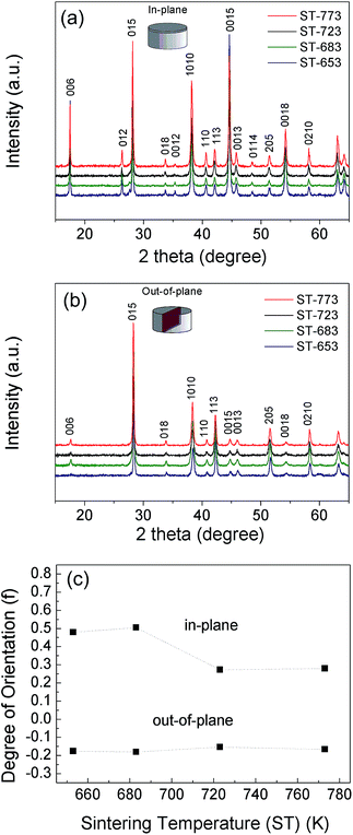 |
| | Fig. 2 Normalized X-ray diffraction patterns of sintered specimens obtained from (a) in-plane surfaces, planes perpendicular to the pressure axis, and (b) out-of-plane surfaces, planes parallel to the pressure axis. The patterns from top to bottom are measured from 773 K, 723 K, 685 K, and 653 K specimens, respectively. (c) Degree of orientation calculated from X-ray diffraction patterns using eqn (1). | |
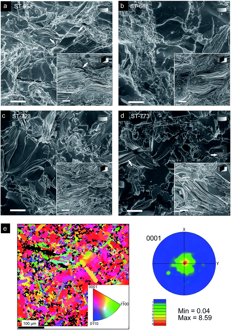
In order to elucidate the microstructure evolution when having variable sintering temperatures, the SEM images were taken from the fractured surfaces of the samples as shown in Fig. 3. The surfaces perpendicular to the pressure axis give the out-of-plane views, whereas the in-plane views are shown in the insets for comparison. The lamina-like structures are clearly observed from the in-plane views. On contrary, the out-of-plane views hardly show any laminated structures for all the samples, which is consistent with the degrees of orientation measured from the XRD spectrums. In Fig. 3a, the 653 K sample has pores and gaps at the grain boundaries with the size of a few hundred nanometers to several microns (pointed with arrows in the figure), whereas the other samples have no such gaps under SEM observations. This is mainly caused by the change of mass density between 653 K and 683 K. After 683 K, grain growth can be observed especially for the small grains with the size of a few microns in ST-683 sample. They merge into larger grains with different orientations at higher temperature. In ST-773 sample, some lamina-like structures can be seen even from the out-of-plane fracture surfaces as pointed out in Fig. 3d. In addition, some metallic droplets were squeezed out of graphite die after SPS at 723 K and 773 K, (see Fig. S6 in ESI†). The SEM-EDS elemental mapping showed negligible changes to the element compositions between ST-653 and ST-773 (see Table 2 and Fig. S2 and S3 in ESI†). Noticeably, the Te concentration is slightly richer in the spilled droplets than the bulk sample. The reason can be the inhomogeneity in the bulk sample which caused Te that has a lower melting point selectively melted and being squeezed out of the sample. A similar liquidifying phenomenon has been observed in recent publications,11 where the amount of Te was significantly higher due to the excessive Te in the bulk samples. In order to confirm the texture in these samples, an EBSD orientation mapping was performed on a fine polished ST-773 sample surface perpendicular to the pressure axis in SPS (see Fig. 3e). The results revealed a significant texture of the grains with {0001} orientation. The quantitative results showed the fraction of those grains with {0001} orientation to be ∼25%, which is consistent with the degrees of orientation calculated from XRD spectrum. The formation of preferential orientations of {0001} can mainly ascribed to significant axial strain in the SPS process. Texture can develop due to slip, grain boundary sliding, grain rotations and dynamic recrystallization. A detailed illustration will be shown later.
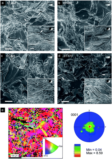 |
| | Fig. 3 SEM images from the fracture surfaces perpendicular to the pressure axis. The sample specimens shown from (a) to (d) were sintered at 653 K, 683 K, 723 K, and 773 K, respectively. The inset images are from the fracture surfaces parallel to the pressure axis. The scale bars are 20 μm. (e) Left: color coded inverse pole figure (IPF) map showing the grains of the ST-773 specimens along the surface perpendicular to uniaxial pressure. The color code corresponds to the crystallographic orientation with {0001} normal to the observation area (as given in the inserted stereographic triangle). Right: pole figure and calculated orientation densities. | |
Table 2 Quantitative analysis results from SEM-EDS element mappings
| Samples |
Bi |
Te |
Sb |
| ST-653 |
8.2% |
61.2% |
30.6% |
| ST-773 |
8.2% |
60.6% |
31.2% |
| Spilled droplets |
6.5% |
62% |
31.5% |
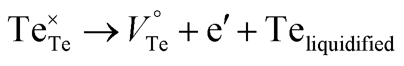
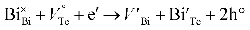
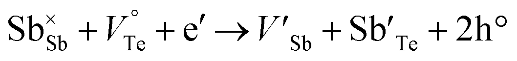
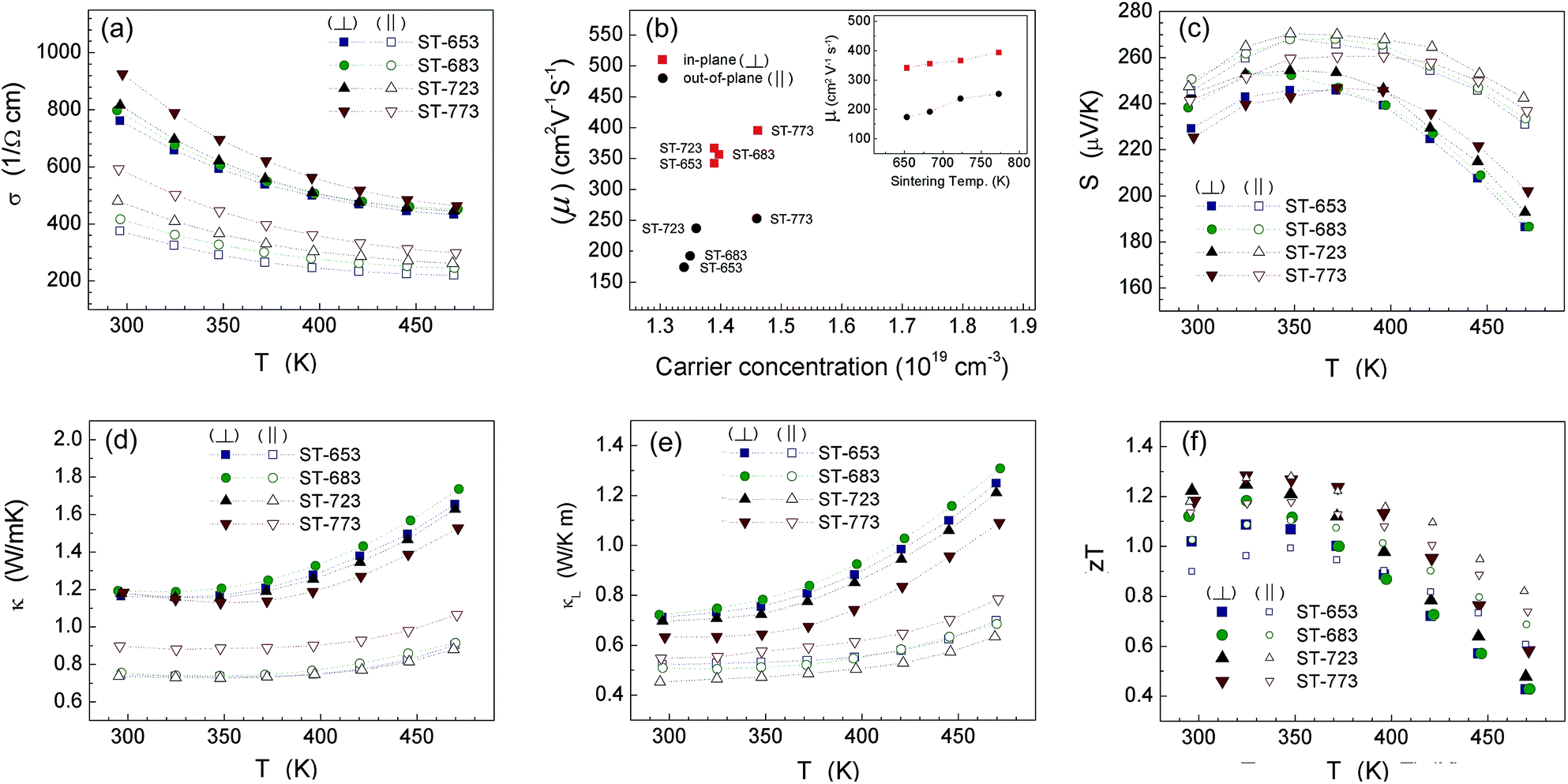
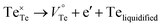
The measured TE properties of the specimens sintered at 653, 683, 723, and 773 K are shown in Fig. 4. The electrical conductivity (σ) measured perpendicular to the pressure axis is notably higher than the ones parallel to the pressure axis by a factor of 2, as shown in Fig. 4a. σ increased as the sintering temperature increased regardless of the measurement directions. This can be attributed to the monolithic increase of carrier mobility (μ) as a function of sintering temperature shown in Fig. 4b. According to the previous microstructure observations in the study, the grain growth at higher temperature apparently resulted in less grain boundaries, thus reducing the scattering effect. On the other hand, the in-plane carrier mobility is 2 times as high as the out-of-plane carrier mobility for all the samples, which indicates that the electronic transport is favored along the c-plane for this material. As for the carrier concentration, the ST-773 sample has slightly higher carrier concentration than the other samples. This can be due to the promoted reactions of negatively charged antisite defects such as Sb′Te and Bi′Te occupying the vacant Te sites,28 as expressed as follows:
| |  | (2) |
| |  | (3) |
| |  | (4) |
where
eqn (2) represents the liquidification of Te in the main structure when sintered at 773 K, and
eqn (3) and
(4) accounts for the formation of extra holes. As a result, the Seebeck coefficient (
S) for the 773 K sample is slightly smaller than the other samples. As shown in
Fig. 4c, the anisotropy also exists for
S where its values along the perpendicular direction are roughly 10% higher than that along the parallel direction. The origin of the
S anisotropy is related to the material electronic transport properties and the anisotropic scattering effects, which was investigated by Yavorsky
et al.29
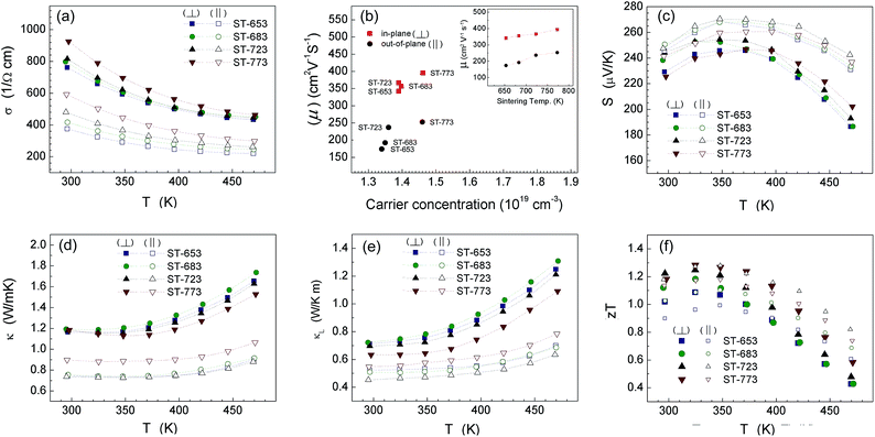 |
| | Fig. 4 TE properties of the specimens sintered at 653 K, 683 K, 723 K, and 773 K. (a) Electrical conductivity, (b) carrier concentration vs. carrier mobility, (c) Seebeck coefficient, (d) thermal conductivity, (e) lattice thermal conductivity and (f) figure-of-merit zT as a function of measurement temperature. | |
Fig. 4d shows the thermal conductivity (κ) of the samples as a function of temperature. The measured data of the specific heat at a constant pressure (Cp) are shown in Fig. S5 in ESI.† The apparent anisotropy on thermal conductivity can be observed from all the samples. The κ values measured along the parallel direction are ∼30% smaller than the values measured along the perpendicular direction over the whole temperature range. These κ values are smaller than previously reported κ values from ingots,9,10 and larger than those of complex nanostructures.9–11 To estimate the lattice contribution κL to the total κ, the following equation was applied:
| | | κL = κ − κe = κ − L0σT | (5) |
where
κe is the electronic component of
κ,
L0 is the Lorenz number. The details for the calculation of Lorenz number is given in the ESI.
† By using
eqn (5), the
κL values can be extracted, as shown in
Fig. 4e. Notably, the ST-773 sample showed higher
κL along the parallel direction and lower
κL along the perpendicular direction than other samples, indicating a smaller anisotropy than other samples due to the decreased degree of orientation by grain growth and re-orientation.
27
The figure-of-merit zT of the samples are shown in Fig. 4f. The ST-723 and ST-773 samples achieved relatively higher zT than the other two samples sintered at lower temperatures. This indicates that the grain growth and grain rotations have certain benefits for the improvement of zT by increasing the carrier mobility. There were no major differences between the zT values along the perpendicular direction and the parallel direction. This is because the anisotropic electrical conductivities were passivated by their anisotropic thermal conductivities. However, the average zT values along the perpendicular direction are slightly higher than those along the parallel direction at room temperature. It is noteworthy that the parallel direction has instead higher zT values while measured from 373 to 473 K, e.g. 50.3% higher zT values at 473 K. For all samples, the zT values dropped rapidly as the samples were measured at higher temperatures ∼450 K. This is mainly because of the thermal stimulated bi-polar conduction behavior which decreased the S and increased the κ.
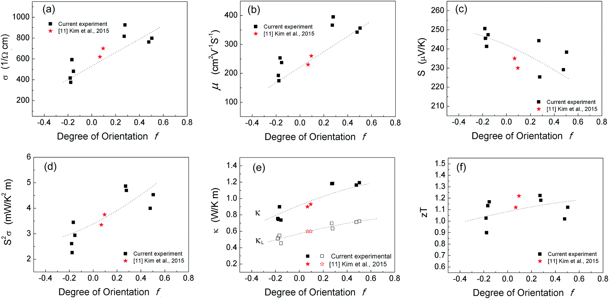
In order to elucidate the influence of preferred orientations on the TE properties of bismuth antimony telluride specimens, the room temperature TE properties measured from both perpendicular and parallel directions were plotted as a function of the degree of orientation, as shown in Fig. 5. The degrees of orientation (f) of the specimens were calculated from the X-ray diffraction patterns. The sample orientation shows significant influence to the TE properties. In Fig. 5a, the σ changed from 400 ohm−1 cm−1 to 800 ohm−1 cm−1 by average when the degree of orientation changed from −0.2 to 0.5. This change can be well explained by the change of μ as a function of f in Fig. 5b. The literature results (nominal bismuth antimony telluride by SPS) from Kim et al.11 are consistent with our results. The Seebeck coefficient (S) shows also some anisotropy. The out-of-plane S values are slightly larger than that of the in-plane, as shown in Fig. 5c. The power factor (S2σ) has a negative correlation to the degrees of orientation. In Fig. 5d, the samples with positive f have significantly larger S2σ than the samples with negative f. However, the κ and κL increase monolithically with the increasing f, as shown in Fig. 5e. The overall zT shown in Fig. 5f does not show significant difference with f. The zT values of above 1.2 at room temperature was achieved by both of the in-plane and out-of-plane sample, which is comparable to the nominal bismuth antimony telluride literature results.11
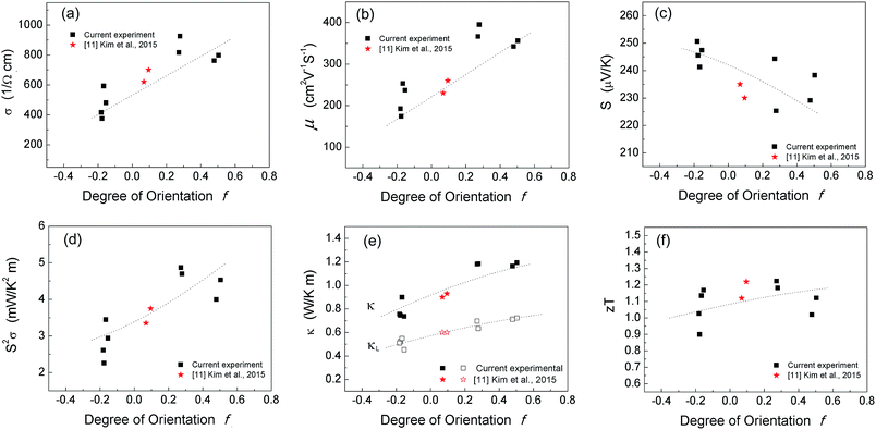 |
| | Fig. 5 Room temperature TE properties plotted as a function of the degree of orientation: (a) electrical conductivity, (b) carrier mobility, (c) Seebeck coefficient, (d) power factor, (e) thermal conductivity, and (f) figure-of-merit zT of the sintered specimens. The stars are reference values from literature11 for comparison. The dotted lines are only guide to the eyes. | |
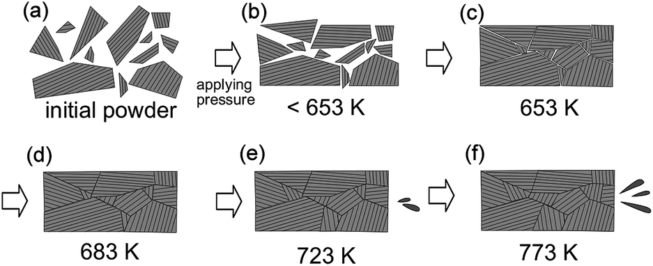
According to the former characterizations and discussions, one can use a simplified illustration to explain the microstructural evolution during SPS, as shown in Fig. 6. The high anisotropy was observed for sample sintered 653 K, therefore the first particle/grain alignment took place already before 653 K due to the uniaxial pressure (see Fig. 6b and c). The complete densification happened at 683 K sample in correspondence with the mass density measurement (see Fig. 6d). The second change in grain alignment took place around 723 K by grain growth and re-orientation (see Fig. 6e). As a result, the anisotropy of lattice thermal conductivity was decreased, and the carrier mobility as well as electrical conductivity was increased. At 773 K, carrier concentrations slightly increased due to the promoted chemical reactions, e.g. the formation of Bi′Te, Sb′Te antisites at the grain boundaries. The softening and the squeezing out Te-rich compounds became more pronounced, shifting the grains to more randomized orientations (see Fig. 6f). However, higher sintering temperature was not performed in this work due to the higher pressure built in the sample during sintering and the limitation of the graphite die strength.
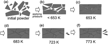 |
| | Fig. 6 Schematic illustrations of microstructural grain alignment evolution during SPS: (a) initial powder before applying uniaxial pressure, (b) open porous structure when T < 653 K after applying pressure, (c) early state of sintering at 653 K, bulk sample with closed pores and gaps (d) dense bulk at 683 K, (e) dense bulk at 723 K, grain growth and re-orientation changes the degrees of orientation, and (f) dense bulk with increased grain growth at 773 K, softened bulk samples are squeezed out. | |
Influence of holding time
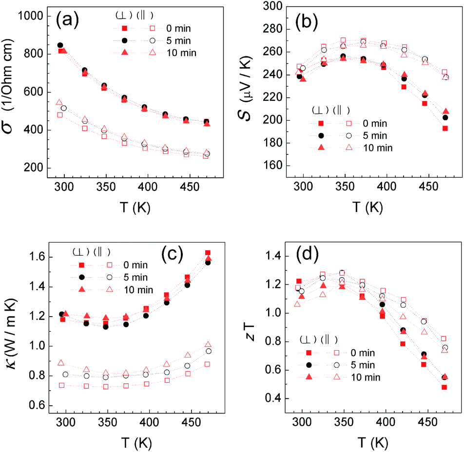
The investigations of holding time during the SPS process on the TE properties were all performed at 723 K, the corresponding sintering profile, mass density, degree of orientation were shown in Fig. S7 in ESI.† The samples sintered at 723 K did not shown significant differences in the mass density and degrees of orientations with variable holding time, except when the holding time reached 10 minutes, a slight change in the degree of orientation could be noticed. This can be due to the grain growth and re-orientation caused by the long holding time, despite the fact that the change was so small that their TE properties were very similar to each other. The TE properties of the samples shown in Fig. 7 also suggested minor differences among the samples sintered at 723 K with variable holding time.
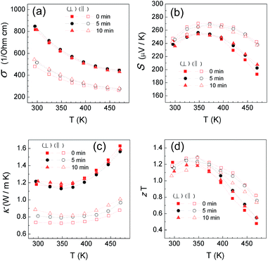 |
| | Fig. 7 TE properties for SPS sintered samples at 723 K with variable holding time. | |
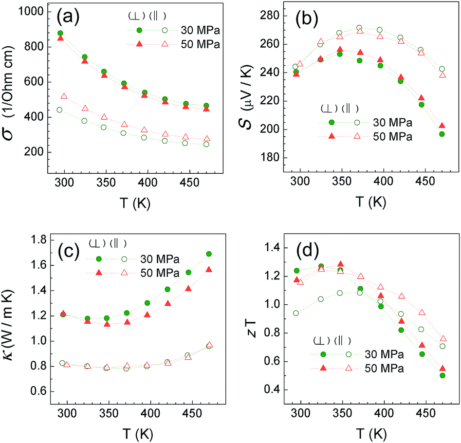
Influence of pressure
The investigations of uniaxial pressure of SPS were performed by comparing the samples sintered under a lower pressure of 30 MPa and a normal pressure of 50 MPa. Using 30 MPa, the resultant anisotropy is slightly higher than that using 50 MPa according to the degrees of orientation shown in Fig. S8c in ESI.† This can be due to the slower displacement when using less pressure as shown in Fig. S8a,† which also indicates a slower grain growth and grain rotations, despite the fact that the final mass density of the samples are nearly the same.
Overall, the anisotropy was already very pronounced even when the pressure was as low as 30 MPa. Additionally, the influence of the uniaxial pressure on the TE properties was shown in Fig. 8. The unexpected low zT for 30 MPa sample (in parallel direction) was obtained mostly due to the lower electrical conductivity than the 50 MPa sample. It would be possible that a higher pressure is beneficial for the electrical transport along the parallel direction to the pressure axis.
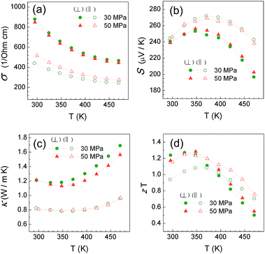 |
| | Fig. 8 TE properties for SPS sintered samples with variable uniaxial pressure. | |
Influence of ramp-rate
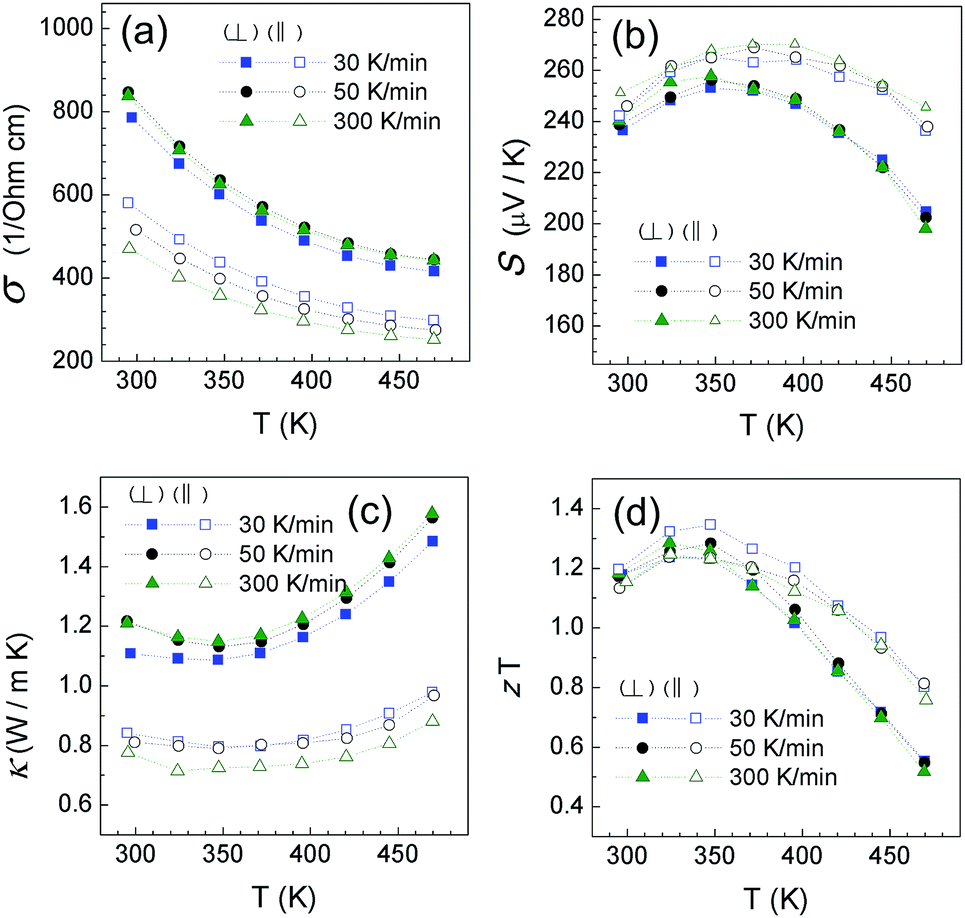
The influences of ramp-rate during SPS were investigated while keeping the same sintering temperature at 723 K, holding time of 5 min, and uniaxial pressure of 50 MPa. The sintering profile in Fig. S9 in ESI† shows that the peak sintering current was different in a factor of 2 between the high ramp-rate 300 K min−1 sample and the low ramp-rate 30 K min−1 sample. The high ramp-rate shortened the total sintering time for 300 K min−1 sample to less than 400 seconds. The high ramp-rate also resulted in a slightly higher degree of orientation in the 300 K min−1 sample, which can also relate to the increased anisotropy in electrical conductivity and thermal conductivity for the 300 K min−1 sample as shown in Fig. 9a and c, respectively. However the high current as well as high ramp-rate had very limited influences on the overall TE properties. On the other hand, the 30 K min−1 sample benefited from the improved out of plane electrical conductivity due to a smaller anisotropy (see Fig. S9c in ESI†), which resulted in a slightly high out-of-plane zT values than other samples. Nevertheless, the maximum zT as for holding time, pressure and ramp-rate seems to remain constant at approximately 1.3@350 K. The detailed TE properties of the samples with variable ramp-rates are shown in Fig. 9.
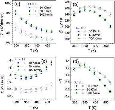 |
| | Fig. 9 TE properties for SPS sintered samples with variable ramp-rate. | |
Conclusion
Variable SPS sintering conditions have been investigated for the preparation of bismuth antimony telluride. The changes of microstructure evolution during SPS were illustrated and related to the TE properties of the materials measured at different directions. The sintering temperature showed major influences to the anisotropy and TE properties of bismuth antimony telluride. Sintering temperature below 683 K resulted in samples with high anisotropy and not fully densified samples with closed pores and gaps at the grain boundaries. Therefore their TE performances were not optimized. Sintering temperature above 723 K resulted in dense samples with slightly lower anisotropy. Additionally, the squeezing out of Te-rich compounds and grain growth and re-orientation were observed. The grain growth increased the carrier mobility by having less grain boundaries. zT values above 1.2 at 300 to 360 K were achieved by samples sintered at 723 K and 773 K despite the measurement directions. The other sintering parameters, i.e. holding time, uniaxial pressure, and ramp-rate had very limited influences on the overall TE properties of the samples. The current work gives an insight to the influence of SPS sintering conditions on the anisotropy of TE properties of bismuth antimony telluride and shows an additional way to control the TE properties of this material.
Acknowledgements
The authors thank the European Union's Seventh Programme for research, technological development and demonstration (grant agreement No. 604647) for sponsoring the current work which is part of the NanoCaTe research project.
References
- G. J. Snyder and E. S. Toberer, Nat. Mater., 2008, 7, 105–114 CrossRef CAS PubMed.
- J. R. Sootsman, D. Y. Chung and M. G. Kanatzidis, Angew. Chem., Int. Ed., 2009, 48, 8616–8639 CrossRef CAS PubMed.
- H. Goldsmid, Materials, 2014, 7, 2577–2592 CrossRef CAS PubMed.
- M. S. Dresselhaus and L. E. Bell, Nat. Nanotechnol., 2013, 8, 469 CrossRef PubMed.
- H. J. Goldsmid and R. W. Douglas, Br. J. Appl. Phys., 2002, 5, 458 CrossRef.
-
D. M. Rowe, CRC Handbook of Thermoelectrics, New York, 1995, vol. 16, pp. 1251–1256 Search PubMed.
- W. Xie, J. He, H. J. Kang, X. Tang, S. Zhu, M. Laver, S. Wang, J. R. D. Copley, C. M. Brown, Q. Zhang and T. M. Tritt, Nano Lett., 2010, 10, 3283–3289 CrossRef CAS PubMed.
- H. Goldsmid, Materials, 2014, 7, 2577–2592 CrossRef CAS PubMed.
- Y. Ma, Q. Hao, B. Poudel, Y. Lan, B. Yu, D. Wang, G. Chen and Z. Ren, Nano Lett., 2008, 8, 2580–2584 CrossRef CAS PubMed.
- B. Poudel, Q. Hao, Y. Ma, Y. Lan, A. Minnich, B. Yu, X. Yan, D. Wang, A. Muto, D. Vashaee, X. Chen, J. Liu, M. S. Dresselhaus, G. Chen and Z. Ren, Science, 2008, 320, 634–638 CrossRef CAS PubMed.
- S. Il Kim, K. H. Lee, H. A. Mun, H. S. Kim, S. W. Hwang, J. W. Roh, D. J. Yang, W. H. Shin, X. S. Li, Y. H. Lee, G. J. Snyder and S. W. Kim, Science, 2015, 348, 109–114 CrossRef PubMed.
- E. G. Dzhafarov, T. D. Alieva and D. S. Abdinov, Neorg. Mater., 2001, 37, 182–185 CrossRef.
- N. Van Nong, N. Pryds, S. Linderoth and M. Ohtaki, Adv. Mater., 2011, 23, 2484–2490 CrossRef CAS PubMed.
- H. Search, C. Journals, A. Contact and M. Iopscience, J. Phys.: Condens. Matter, 1997, 9, 461 CrossRef.
- M. Takashiri, S. Tanaka and K. Miyazaki, Thin Solid Films, 2010, 519, 619–624 CrossRef CAS.
- L. Han, N. Van Nong, W. Zhang, L. T. Hung, T. Holgate, K. Tashiro, M. Ohtaki, N. Pryds and S. Linderoth, RSC Adv., 2014, 4, 12353 RSC.
- X. Yan, B. Poudel, Y. Ma, W. S. Liu, G. Joshi, H. Wang, Y. Lan, D. Wang, G. Chen and Z. F. Ren, Nano Lett., 2010, 10, 3373–3378 CrossRef CAS PubMed.
- D. Teweldebrhan, V. Goyal and A. A. Balandin, Nano Lett., 2010, 10, 1209–1218 CrossRef CAS PubMed.
- J. Ko, J.-Y. Kim, S.-M. Choi, Y. S. Lim, W.-S. Seo and K. H. Lee, J. Mater. Chem. A, 2013, 1, 12791 RSC.
- L. Han, L. T. Hung, N. Nong, N. Pryds and S. Linderoth, J. Electron. Mater., 2012, 42, 1573–1581 CrossRef.
- N. Wu, T. C. Holgate, N. Van Nong, N. Pryds and S. Linderoth, J. Eur. Ceram. Soc., 2014, 34, 925–931 CrossRef CAS.
- J. G. Noudem, D. Kenfaui, D. Chateigner and M. Gomina, J. Electron. Mater., 2011, 40, 1100–1106 CrossRef CAS.
- J. Jiang, L. Chen, S. Bai, Q. Yao and Q. Wang, Mater. Sci. Eng. B, 2005, 117, 334–338 CrossRef.
- H. Böttner, D. G. Ebling, A. Jacquot, J. König, L. Kirste and J. Schmidt, Phys. Status Solidi RRL, 2007, 1, 235–237 CrossRef.
- M. Gharsallah, F. Serrano-Sánchez, J. Bermúdez, N. M. Nemes, J. L. Martínez, F. Elhalouani and J. A. Alonso, Nanoscale Res. Lett., 2016, 11, 142 CrossRef CAS PubMed.
- S. Tanaka, A. Makiya, T. Okada, T. Kawase, Z. Kato and K. Uematsu, J. Am. Ceram. Soc., 2007, 90, 3503–3506 CrossRef CAS.
- R. D. Doherty, D. A. Hughes, F. J. Humphreys, J. J. Jonas, D. Juul Jensen, M. E. Kassner, W. E. King, T. R. McNelley, H. J. McQueen and A. D. Rollett, Mater. Today, 1998, 1, 14–15 CrossRef.
- L. P. Hu, X. H. Liu, H. H. Xie, J. J. Shen, T. J. Zhu and X. B. Zhao, Acta Mater., 2012, 60, 4431–4437 CrossRef CAS.
- B. Y. Yavorsky, N. F. Hinsche, P. Zahn and I. Mertig, Phys. Rev. B: Condens. Matter Mater. Phys., 2011, 84, 165208 CrossRef.
Footnote |
| † Electronic supplementary information (ESI) available: Supplement SEM images, SPS sample cutting schematics, heat capacity, calculation of Lorenz number, etc. See DOI: 10.1039/c6ra06688g |
|
| This journal is © The Royal Society of Chemistry 2016 |
Click here to see how this site uses Cookies. View our privacy policy here. 
 Open Access Article
 This Open Access Article is licensed under a