
Strengthening of liquid crystal photoalignment on azo dye films: passivation by reactive mesogens
Man-Chun
Tseng
a,
Oleg
Yaroshchuk
*ab,
Tetyana
Bidna
b,
Abhishek Kumar
Srivastava
*a,
Vladimir
Chigrinov
a and
Hoi-Sing
Kwok
a
aState Key Laboratory on Advanced Displays and Optoelectronics Technologies, The Hong Kong University of Science and Technology, Clear Water Bay, Kowloon, Hong Kong. E-mail: o.yaroshchuk@gmail.com; abhishek_srivastava_lu@yahoo.co.in
bDept. of Physics of Crystals, Institute of Physics, NASci. of Ukraine, prospekt Nauki 46, 03680 Kyiv, Ukraine
First published on 3rd May 2016
Abstract
Disazo dyes form a highly effective class of liquid crystal (LC) photo-aligning materials whose molecules undergo fast orientation or reorientation under exceptionally low irradiation doses. These properties make these materials irreplaceable for application in all-optical LC devices. At the same time, the high sensitivity of the photo-orientation prevents the extension of this method to electro-optical elements such as LC displays and photonic devices. To stabilize LC alignment on dye films, several approaches have been developed which employ reactive mesogens (RMs) capable of photopolymerization. This article comprehensively describes the approach associated with the passivation of photoaligning films by thin layers of RMs. It is shown that continuous RM films with a thickness ≥5 nm provide highly uniform, thermally and photo-stable LC alignment. This approach also provides a VHR of more than 99%, RDC voltage less than 5 mV, and image sticking parameter about 1.002, which are the same as for rubbed polyimide films. Together with the low pre-tilt angle, high anchoring energy and ability of alignment patterning, this makes the proposed approach promising for application in a range of electro-optical devices, particularly those requiring active matrix driving and multi-domain alignment.
1. Introduction
Alignment of liquid crystal (LC) molecules at boundary substrates is a key factor determining the optical quality and electro-optical performance of liquid crystal displays (LCDs). Until recently, the only method of LC alignment, on an industrial scale, was unidirectional rubbing of polymer boundary layers. However, recent years have seen rapid growth of the popularity of another method called photoalignment.1,2 This method, proposed at the beginning of the 1990's, has caused a new surge of interest after a series of its recent industrial applications in displays and photonics. However, these materials are still not mature and further research is required for the development of a new generation of photoaligning materials providing desirable aligning parameters and dielectric characteristics. One of the most promising classes of these materials is formed by disazo dyes. The chemical formula of the most common representative of this class, sulphonic disazo dye SD1, is given in Fig. 1. This dye provides excellent alignment for LCs3 and reactive mesogens (RMs),4 with strong anchoring and controllable pretilt angle. Alignment (realignment) of LC layers by using such materials can be achieved at exceptionally low irradiation energy doses of ∼10 mJ cm−2. The re-orientation ability has been successfully exploited for optically addressed (optically rewritable) displays providing 2D and 3D contents5,6 and diffraction gratings with a very high spatial resolution (<100 nm).7 On the other hand, the high photosensitivity of azo dye films prevents their application in conventional electrically driven displays and other photonic devices where high alignment stability is required.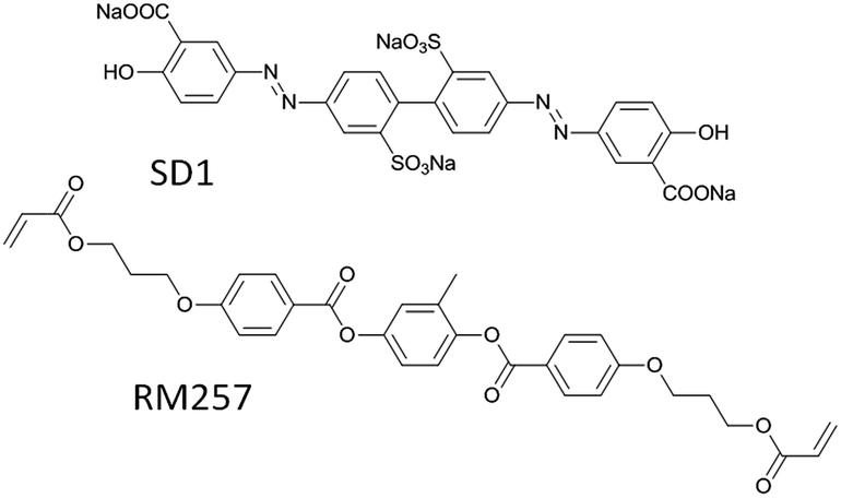 | ||
| Fig. 1 Chemical structures of photoaligning dye SD1 and reactive mesogen RM257. | ||
To overcome this limitation, several approaches have been explored. They are unified by the general idea of fixing the photoaligned azo molecules by various ways of crosslinking. The first approach consists in the attachment of crosslinking fragments to azo dye molecules. The implementation of this approach has shown strengthening of the alignment stability; however, it was accompanied by worsening of the alignment quality.8 This has motivated the use of other molecules with crosslinking groups such as the molecules of reactive mesogens. There are three especially popular approaches. The first approach is connected with the separation of RM from LC and the formation of an RM network on the photoalignment layers. Initially, such an approach was proposed to set the pretilt angle and speed up the electro-optic response of LC displays with vertical alignment.9,10 Also of note is ref. 11, in which this method was applied to reduce residual DC voltage in cells with planar alignment based on photoaligning polyimide films. The application of this method to stabilize the LC alignment of the layers of disazo dyes was suggested in ref. 12. In this work, a small amount (1–2 wt%) of RM was dissolved in LC and this mixture was filled in a cell containing photoaligning layers of disazo dye. The dissolved molecules of RM concentrated near the aligning substrates due to effective adsorption and gradient of light in the photopolymerization process. As a result, thin layers of polymerized RMs were formed on the aligning substrates. It was shown that this approach can be effectively applied even in the case of pre-manufactured cells with the dye photoaligning films. Its weak point lies in the fact that some portion of the RM molecules may remain in the LC and act as an impurity. The second approach, initially suggested to control the pretilt angle in various types of LC displays,13,14 is associated with mixing of alignment material and RM. To stabilize LC alignment on disazo dye photoalignment films, such an approach was proposed in ref. 15. It has been shown that the alignment layers based on the mixture of disazo dye and RM in an optimized proportion provide essentially enhanced photo- and thermal stability and perfectly suit ferroelectric LCs. The third approach considers a coating of RM layer over the aligning films. Its history can be traced back to the beginning of the 90s when an auxiliary layer of RM was used to amplify the pretilt angle of LC on the rubbed polyimide films.16 It has recently been shown that this procedure may also modify the anchoring energy of LC on the rubbed surfaces.17 Application of this approach to stabilize LC alignment on the films of disazo dyes was proposed in our earlier work.18 In this case, the dye layer aligns the RM, whereas the latter aligns the LC in the bulk. Before bringing in contact with LC, the aligned layer of RM is subjected to photo-crosslinking to make it insoluble in LC and fix the positions of RM molecules. The aligned and highly crosslinked layer of RM, in turn, provides stable alignment of LC. Furthermore, the layer of RM performs additional functions; it serves as a barrier layer protecting hygroscopic SD1 film from destructive moisture and prevents injection of ions from the dye in the LC bulk.
Ref. 18 illustrates the principle of such an approach. However, further comprehensive research is required in order to make electrical and optical parameters of the cells based on the developed aligning layers compatible with the modern active matrix driving technology. In this article we study the effect of thickness and processing conditions of passivation layers on the alignment characteristics and electro-optic performance of LC cells. It has been found that the thickness optimization and special processing environment improve all the vital parameters, which become comparable to the rubbed polyimide layers. This makes the proposed alignment layers extremely promising for a range of photonic and LC display applications.
2. Experimental
2.1. Alignment layers and LC cells
In this research we used SD1 dye from DIC, which is a frequently used photoaligning dye known for exceptional alignment properties and high thermal stability of the induced LC alignment. The SD1 was dissolved in dimethylformamide (DMF) at a concentration of 0.5 wt% and filtered to 0.2 µm. Afterwards, the solution was spin-coated at 3000 rpm onto glass substrates containing continuous ITO electrodes or patterned Cr electrodes for in-plane switching (IPS), preliminarily thoroughly washed and cleaned in an ozone treatment machine. The coated layers were annealed at 110 °C over 15 min for complete removal of DMF and then exposed to linearly polarized UV light from a mercury lamp. The intensity of UV light was 1.3 mW cm−2 in the 365 nm emission line and the time of irradiation was 5 min. To avoid two-fold degeneration of the pre-tilt angle2 the substrates were irradiated slantwise at an angle of 45° with s-polarization of the light. This procedure appeared to be very effective for the studied dyes, seemingly because of the imperfect polarization and high photosensitivity of the dye molecules.We initially tested several reactive mesogens such as RMM256C and RM257 from Merck and UCL017 from DIC as a passivating agent. Based on the experimental results, we found that the RM257 provides the most stable and uniform coatings over the dye films. Therefore, in consequence, this material was used. Its molecular structure is presented in Fig. 1. The sequence of phases of RM257 is crystal-nematic-isotropic with the transition temperatures 71 °C and 128 °C, respectively.19 The material was doped with 3 wt% of photo-initiator Irgacure 651 (Chiba) and then dissolved in toluene. The concentration of RM, CRM, was varied in the range 0–5 wt%. The filtered solution was spin-coated onto the photoaligning films to form the passivation films. Subsequently, the RM films were exposed to UV light from a mercury lamp with an intensity of 12 mW cm−2 at a 365 nm emission spectrum for 5 min to provide the saturated photopolymerization.
It was established that for the exposure time τex < 3 min the RM film can be realigned with the SD1 commanding layer located underneath it, while for τex > 5 min the alignment of RM does not show any changes. The latter means that the photoinduced reorientation of SD1 molecules does not lead to reorientation of RM, because the degree of crosslinking for RM is sufficiently high to maintain the initial alignment. Proceeding from this, the exposure time for photopolymerization was fixed to 8 min. After the photopolymerization, the films were annealed at 100 °C for 10 min to complete the evaporation of toluene. The annealing was deliberately executed after photopolymerization to prevent the formation of a hybrid alignment structure with homeotropic alignment at the RM–air interface,20,21 which eliminates the LC alignment ability of such films.
To prepare rubbed polyimide (PI) films we used PI-3744 for planar alignment from Chisso Co. The spin-coated films of this polyimide were backed at 230 °C for 1 h and then unidirectionally rubbed using a rayon-cloth rubbing machine at 250 rpm rotation speed of the rubbing drum, 20 mm s−1 translation speed of the films and a pile impression of 0.5 mm.
The substrates with SD1/RM or rubbed polyimide (PI) aligning films were used to assemble two kinds of cells, with the exposure directions in the photoaligning process being antiparallel or perpendicular to each other (i.e. antiparallel and twist cells, respectively). The cell thickness dLC was adjusted by spacers with a diameter of 5 or 20 µm. The cells were filled with the nematic LC E7 or MDA-01-4679 from Merck at 50 °C. The antiparallel cells with ITO electrodes having thickness dLC = 20 µm were used to estimate the pre-tilt angle and polar anchoring energy, while those with IPS electrodes and thickness dLC = 5 µm were involved in electro-optic and image sticking measurements. The twist cells (dLC = 5 µm) with ITO electrodes were used for estimation of the azimuthal anchoring, voltage holding ratio (VHR) and residual direct current (RDC) voltage. Similar cells combining one rubbed PI alignment and another photoalignment, i.e. SD1/RM films, were used to test the photo-stability.
2.2. Experimental methods
The nanomorphology of the passivating RM films was studied using a scanning atomic force microscope (AFM) Nanoscope IIIa (Digital Instruments) operating in non-contact mode. Surface areas with a size of 5 × 5 µm were analyzed. The scanning direction was either parallel or perpendicular to the alignment direction of RM.The alignment of RM molecules within the films was also explored by transmission null ellipsometry, which can be considered as the Senarmont technique generalized for oblique incidence of the testing light. The high efficiency of this technique was earlier demonstrated for thin anisotropic films of LCs and photosensitive polymers.20–22 The optical arrangement of the method is presented in Fig. 2a. The beam of testing light with a wavelength of 633 nm is linearly polarized at 45° with respect to the anisotropy axes of the sample. After passing through the anisotropic sample, the beam becomes elliptically polarized. The quarter wave plate with an axis parallel to that of the polarizer further transforms light into the linearly polarized state with the axis of polarization rotated by some angle φ with respect to the polarization direction at the entrance to the system. The angle φ is determined by analyzer rotation to the state corresponding to minimal transmittance of the optical system. The analyzer angle φ is experimentally measured as a function of the sample rotation angle θ. The fitting of this curve yields the spatial orientation of the refractive index ellipsoid and both in-plane (ny − nx)d and out-of-plane (nz − nx)d retardations, allowing an estimate of the ratio of the principal components of the refractive index tensor. This, in turn, allows us to reconstruct the spatial alignment configuration of anisotropic molecular units. The obtained value of the in-plain retardation was also used to determine the thickness of RM passivating films.
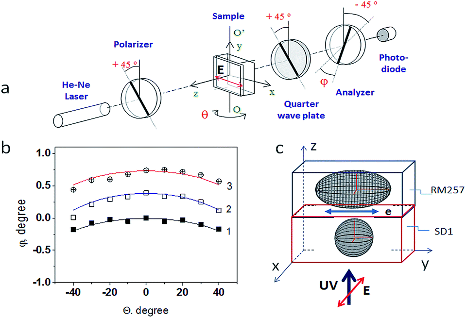 | ||
| Fig. 2 (a) Optical arrangement of transmission null ellipsometry. (b) Analyzer angle vs. sample rotation angle curves for the spin-coated SD1 film before (curve 1) and after (curve 2) exposure to polarized UV light, and for the stack of the exposed SD1 film and the film of RMM257 applied on top of it (curve 3). Both films are spin-coated from 0.5 wt% solution at 3000 rpm. Symbols are experimental points and the lines are fitting curves. The fitting results for cases 1, 2 and 3 are: (1) (ny − nx)d = 0, (nz − nx)d = 3 nm, (2) (ny − nx)d = 1.4 nm, (nz − nx)d = 5.6 nm, and (3) (ny − nx)d = 2.6 nm, (nz − nx)d = 5.8 nm. (c) Refractive index ellipsoids for SD1 and RM films. Vector E is the polarization direction of UV light used for photoalignment processing of SD1 and vector e marks the direction of the easy axis induced in the SD1 film. | ||
The pre-tilt angle of LC was measured by the crystal rotation method.23 The polar anchoring energy was estimated by the modified Yokoyama and van Sprang technique,24,25 while the azimuthal anchoring was determined by the torque balance method based on the twist angle measurement in the twisted cells.26 The VHR and RDC voltage were measured following the procedure described in ref. 15. The VHR for the frame frequency of 60 Hz and temperature 60 °C was estimated by measuring the transmittance of a testing laser beam (633 nm) passed through the LC cell placed between two crossed polarizers. At first, the transmittance vs. voltage curve was measured. Thereafter, an optical response was recorded for the frame time of 16.7 ms after a voltage pulse of 5 V was applied to the cell for 60 µs. The difference in the retardation at the beginning and the end of the frame was used to calculate the VHR. To measure the RDC voltage, first a 5 µm thick cell filled with LC was charged for 1 h at 60 °C by the 10 V DC signal and thereafter the cell was disconnected from the DC source and simultaneously short-circuited for 1 s to discharge the LC capacitor. After this, the residual voltage of the cell was measured for 10 min. The standard value of the RDC voltage has been defined as the magnitude of the residual voltage obtained 10 min after the short-circuiting.15
3. Results and discussion
3.1. Characterization of passivation layers
Before considering the peculiarities of the LC alignment we focus on the structure of the passivating RM films. Film morphology and molecular alignment in the passivating RM films are important to understand the effect of these coatings on the alignment and performance of LC layers and their underlying mechanisms. Primarily, we consider the morphological peculiarities studied by the AFM technique. Three-dimensional AFM images of RM257 films spin-coated on SD1 photoaligning layers from the solutions of various concentrations are presented in Fig. 3. It can be seen that the bare SD1 film and the film coated with RM from 0.06 wt% solution are rather smooth. However, increasing the RM concentration in the solution to 0.13 wt% results in the appearance of pronounced surface features causing high roughness amplitude, which increases to 5 nm at 0.25 wt% concentration. When the RM concentration increases to 0.35 wt%, the films become smooth again. This behaviour indicates that RM coatings develop in several stages. In the case of highly diluted solutions (<0.06 wt%), because of the poor wetting of SD1 films by the diluted solutions, RM material does not form any detectable features on SD1 films. Indeed, the wetting improves with higher concentrations of the RM in solution, which was clearly observed during the coating process. The pronounced features for the concentration range 0.13–0.25 wt% reflect an island structure of the RM coatings, which is apparently formed at moderate wetting of SD1 by RM solution. The height of the features was up to 5.5 nm. Interestingly, the features formed on the SD1 films exposed to polarized light have elongated shape and align in the direction of light polarization (Fig. 4d). This implies wetting anisotropy, with stronger wetting in the direction of light polarization. These surface features disappear for the films obtained from the solutions with CRM ≥ 0.35 wt% and afterwards the film roughness decreases significantly, which suggests that the RM layer becomes continuous for the higher concentration of the RM.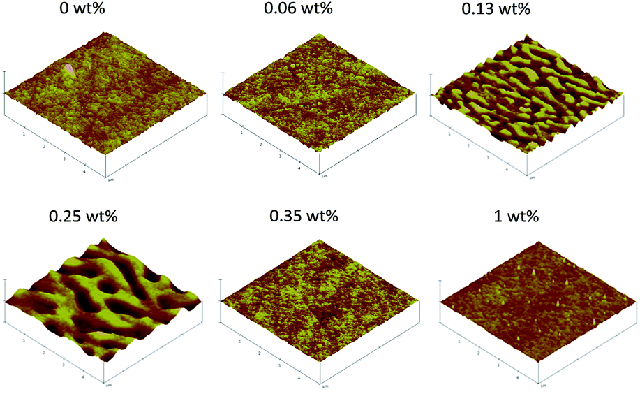 | ||
| Fig. 3 The 3D AFM surface plots for RM257 films spin-coated onto the SD1 photoaligning layers from the solutions of various concentrations of RMM257. For reference, the image of the bare SD1 film obtained from 0.5 wt% solution is added. The SD1 layers are subjected to polarized light irradiation. All films are spin-coated at 3000 rpm for 30 s. | ||
 | ||
| Fig. 4 Illustration of estimation of roughness amplitude da of RM films by AFM. The base figure shows the average amplitude of the roughness as a function of RM concentration in solution. Insets (a) and (b) demonstrate the estimation of roughness by using two arbitrary surface points with maximal and minimal thickness. Insets (c and d): three-dimensional AFM images of RM films spin-coated on the non-irradiated (c) and polarized light irradiated (d) SD1 layer. Polarization direction of light acting on SD1 film is marked by vector E. | ||
The next important issue is the alignment of RM on SD1 film, which sets the alignment of the adjacent LC layer. For these studies we used the null ellipsometry technique, which also allowed us to estimate the thickness of continuous RM films. Fig. 2b shows analyzer angle φ versus sample rotation angle θ curves measured by this method. The curve fitting for non-exposed SD1 film yields (ny – nx)d = 0 and (nz – nx)d = 3 nm, meaning that nz > nx = ny. This ratio of principal indices corresponds to a positive C plate and reflects some preference for out-of-plane ordering of dye molecules. For the exposed SD1 film, the fitting yields (ny – nx)d = 1.4 nm and (nz – nx)d = 5.6 nm. The corresponding ratio nz > ny > nx implies biaxial ordering of SD1 molecules. The retardation introduced by RM coating can be obtained by extraction of the retardation of SD1 film from the total retardation of the SD1 and RM stack. The obtained data (ny – nx)d = 1.2 nm and (nz – nx)d = 0.2 nm suggest the ratio ny > nx ≈ nz, which means uniaxial ordering of RM molecules in the y direction. This result is very reasonable, taking into account the intrinsic uniaxial positive ordering of LCs. The refractive index ellipsoids of adjacent SD1 and RM films are schematically presented in Fig. 2c.
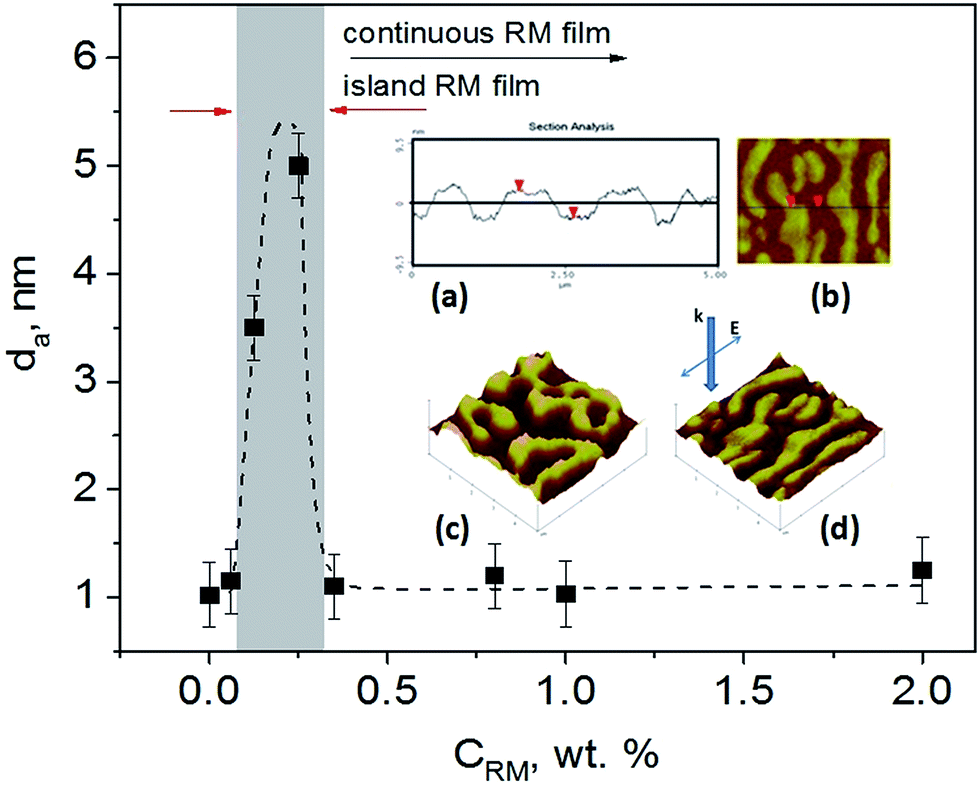
The estimated values of in-plane retardation (ny – nx)d for the aligned RM films were used to calculate the thickness of these films, dRM. In these calculations, the birefringence of RM was assumed to be 0.155.27 The in-plane retardation as a function of RM concentration is presented in Fig. 5, while the calculated thickness vs. CRM curve is shown in the inset of Fig. 5. The open circles here present the thickness data obtained by AFM measurements for discontinuous RM films, i.e. for the concentration CRM less than ≈0.3 wt% (hereinafter this concentration region on the graphs is grayed out). The solid black squares are obtained from the ellipsometry results. Both of these methods show good agreement. Moreover, they supplement each other; the ellipsometry data are non-reliable for discontinuous films, while AFM is not effective for thickness estimation in the case of continuous films. Evidently, thickness changes linearly with the concentration of RM in solution. The minimal thickness of continuous films obtained for CRM = 0.35 wt% was about 5 nm and the maximal value obtained for CRM = 5 wt% was about 90 nm.
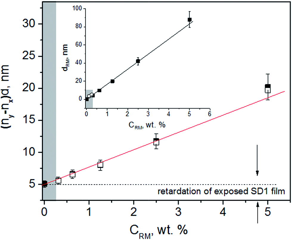 | ||
| Fig. 5 In-plane phase retardation of the stack of SD1 and RM films as a function of RM concentration in toluene solution. Filled and unfilled squares correspond to unpolymerized and polymerized RM films, respectively. Inset: thickness of RM layer as a function of the RM concentration in toluene. The square points are obtained by recalculation of the retardation plot assuming that the birefringence of RM is 0.155.27 The open circles correspond to AFM data deduced from Fig. 4. | ||
3.2. Impact of passivation layers on LC alignment
Despite the fact that ref. 18 shows a positive effect of passivating RM films on the alignment stability, many features remained unclear. First among them is the layer thickness of the RM over the SD1 layer, which will be optimized in this section. This thickness is subject to a trade-off. On the one hand, the RM coating should be thin enough to minimize the undesirable phase shift and scattering losses which they introduce in LC devices. Besides, for ferroelectric LCs, thin aligning films are preferable in order to provide high electrical capacitance.28 On the other hand, their thickness should be sufficiently large to shield the SD1 films and to offer good alignment stability. To study the effect in detail, we have made a series of twisted cells with the SD1 alignment layers covered by RM layers of different thickness.Fig. 6 shows pictures of different twist cells with bare SD1 layers coated with RM films obtained from the solutions of different RM concentrations. To test the photo-stability, all of these cells were illuminated for 1 h with a blue laser light (450 nm, 50 mW cm−2) having linear polarization rotated in the azimuthal plane by 90° with respect to the easy axis on the photoaligning substrate. It can be seen from Fig. 6a that the LC realigns in the cells with the RM passivation layers obtained from the solutions of concentration CRM ≤ 0.25 wt%. This implies that SD1 still continues working as a command material in the filled LC cells even if it is coated with the RM layer. In turn, for the RM concentration CRM ≥ 0.35 wt%, i.e., dRM ≥ 5 nm (Fig. 5), the realignment is not observed even for 1 h of irradiation (see pictures 4 and 5 in Fig. 6a). In other words, the stacked aligning films show very good photo-stability if the RM layers are coated from the solution with CRM ≥ 0.35 wt%, whereas they are not stable for the lower RM concentration. This threshold-like behaviour for the alignment stability can be because of several reasons. One of them is complete screening of SD1 alignment films at some thickness of passivating layer.29,30 However, this process is apparently not expected to offer a threshold-like characteristic. In practice, because of partial screening of photoaligning films, the photosensitivity of the aligning films should vary more smoothly with dRM. The other and much more plausible reason is a discontinuous layer of RM over the SD1 layer. This is well supported by the AFM results; continuous RM films are formed only for CRM ≥ 0.35 wt%. The same threshold concentration is detected in the experiments for alignment stability (Fig. 6). It is reasonable to assume that the areas of SD1 film not covered by RM film continue to work as a command surface for the LC bulk in the cell. The characteristic size of the surface patterns is in the range of tens of nanometers (see Fig. 3) and therefore LC is able to smooth out its alignment so that the alignment patterns are not revealed in the LC bulk.31,32
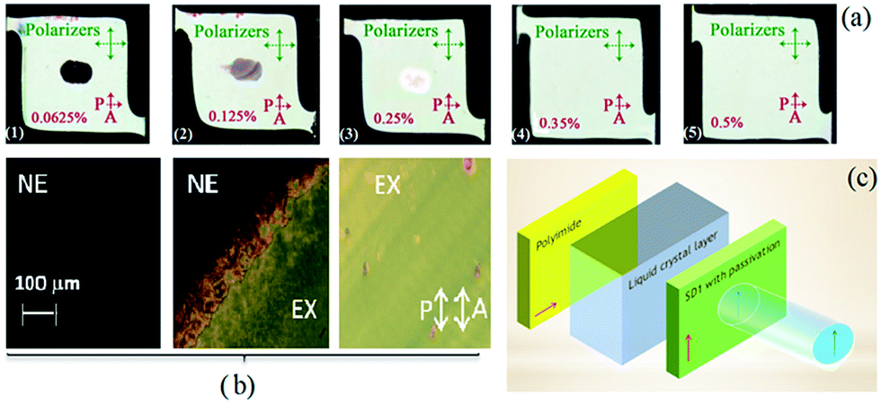 | ||
| Fig. 6 (a) Twist cells containing bottom substrate with rubbed PI layer and upper substrate with photoaligning layer viewed between a pair of crossed polarizers. The photoaligning layer of SD1 is passivated with a thin RM film spin-coated from RM solutions of different concentrations. All cells are filled with LC E7 and then exposed to blue laser light (450 nm, 50 mW cm−2, 1 h) with polarization E2 forming an angle 45° with the polarization E1 used in the first photoalignment processing of SD1 film. Reorientation of LC is visible only in the 1st, 2nd and 3rd cell having discontinuous structure of the passivating RM films (see Fig. 3). (b) Microphotographs of cell 1 taken for the areas non-exposed (NE) and exposed (EX) to laser beam. (c) Schematic of the experimental arrangement to test the photo-stability. | ||
Therefore, one can conclude that an RM layer thickness more than 5 nm offers good photo-stability. However, to deploy these materials for real applications it is important to clarify the influence of the RM thickness on the alignment parameters of LCs. One of them is the pre-tilt angle. We measured the pre-tilt angle for the cells with passivation layers of various thickness filled with LC E7. The pre-tilt angle in these cells fluctuated in the range 0.18–0.21°, which was within the range of experimental error. Thus, it can be advised that the pre-tilt angle of LC E7 is fairly constant and does not show any serious effect from the auxiliary layer of RM257. At the same time, comparison of these results with the results of our previous work18 allows one to conclude that the magnitude of the pre-tilt angle depends on the type of reactive mesogen and the preparation conditions of the RM films, as well as the type of LC filled in the cell.
Another important parameter is the polar anchoring coefficient, Wp. As shown in Fig. 7, it is more sensitive to dRM and reveals clear growth and a tendency to saturation with a thickening of the passivation films. This growth is significant in the range of concentrations corresponding to discontinuous passivating films, but continues even after formation of continuous films. This may suggest that both discontinuity of RM films and screening of photoaligning layers by these films influence Wp. According to Fig. 7, the Wp(CRM) curve comes to saturation at a concentration of about 2 wt% (dRM ≈ 35 nm (Fig. 5)), implying complete screening of SD1 films. This value of dRM is close to the screening thicknesses obtained in ref. 29 and 30. Below, it is shown that the screening trend is also confirmed by the measurement of relaxation time. In contrast to polar anchoring, azimuthal anchoring weakly depends on the thickness of the film (Fig. 7). This may suggest that the anisotropic interaction of LC with SD1 and RM is of comparable strength, possibly because of comparable in-plane orientational order of dye and RM molecules.
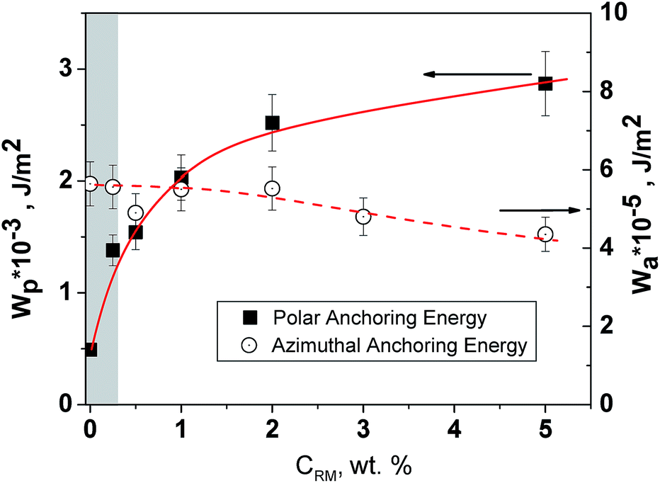 | ||
| Fig. 7 Azimuthal (Wa) and polar (Wp) anchoring energies of the nematic LC E7 as a function of RM concentration in solution used for passivation of SD1 photoaligning films. | ||
3.3. Electro-optic performance
The other important parameters of LC devices, particularly in the case of active matrix driving, are the VHR and RDC voltage. They essentially depend on the electrical properties of the LC and alignment layers. One can anticipate that the introduction of passivating layers in the cells may change their VHR and RDC parameters considerably. To clarify this issue, we used twisted cells (d = 5 µm) with patterned ITO electrodes filled with active matrix LC MDA-01-4679 from Merck possessing high electrical resistivity. The tested samples contained passivation RM layers coated from the 0.35 wt% solution to provide the thinnest continuous RM films (dRM ≈ 5 nm). The reference samples contained either bare SD1 photoaligning layers or rubbed PI films. The VHR and RDC voltage were measured according to the procedure described in Section 2.2. The data are summarized in Table 1.| Properties | Rubbed PI | Non-passivated SD1 | Passivated SD1 |
|---|---|---|---|
| Pre-tilt angle | 0.1–2° | 0.1–0.5° | 0.1–0.5° |
| Polar anchoring energy | 2 × 10⁻³ J m−2 | 0.5 × 10⁻³ J m−2 | (1–3) × 10−3 J m−2 |
| Azimuthal anchoring energy | 1 × 10⁻⁴ J m−2 | 0.6 × 10⁻⁴ J m−2 | (0.4–0.6) × 10−4 J m−2 |
| Voltage holding ratio (60 Hz; 60 °C) | 99.5% | 92% | 99.3% |
| Residual DC voltage (60 °C) | 0.001–0.003 V | 0.08–0.1 V | 0.002–0.005 V |
| IS | ++ | − | ++ |
| Stability | ++ | −− | ++ |
| Multi-domain alignment ability | −− | ++ | ++ |
In agreement with previous data,18 bare SD1 films provide inferior parameters compared with rubbed PI films – insufficient value of VHR (96–98%) and rather high RDC voltage (50–60 mV). This may be caused by intrinsic charges in SD1, since this material is an organic salt. The passivation with RM improves these values considerably. Furthermore, optimization efforts, aimed at maximization of the degree of polymerization, resulted in even better VHR and RDC values, comparable with and sometimes better than the values for rubbed PI. The VHR and RDC for the optimized passivated SD1 layers reached 99.3% and 0.002 V, respectively, which are similar to those for the rubbed PI with 99.5% and 0.001 V, respectively.
The same cells were used to estimate the time of orientational relaxation after switching off the electric field. For the cells containing bare SD1 and PI alignment layers, this time is 36.4 ms and 27.2 ms, respectively. After passivation of SD1 films the relaxation time decreases from 36.4 ms to 30.6 ms. This supports the above conclusion about the strengthening of polar anchoring for passivated films.
Fig. 8 shows transmittance, T, vs. voltage, V, curves measured for IPS cells with bare SD1, rubbed PI and passivated SD1 alignment layers (Fig. 8(a), (b) and (c), respectively). Disregarding the features of hysteresis, one can conclude that passivation of SD1 layers with RM does not change the T–V curves considerably. In particular, the controlling voltage remains practically intact.
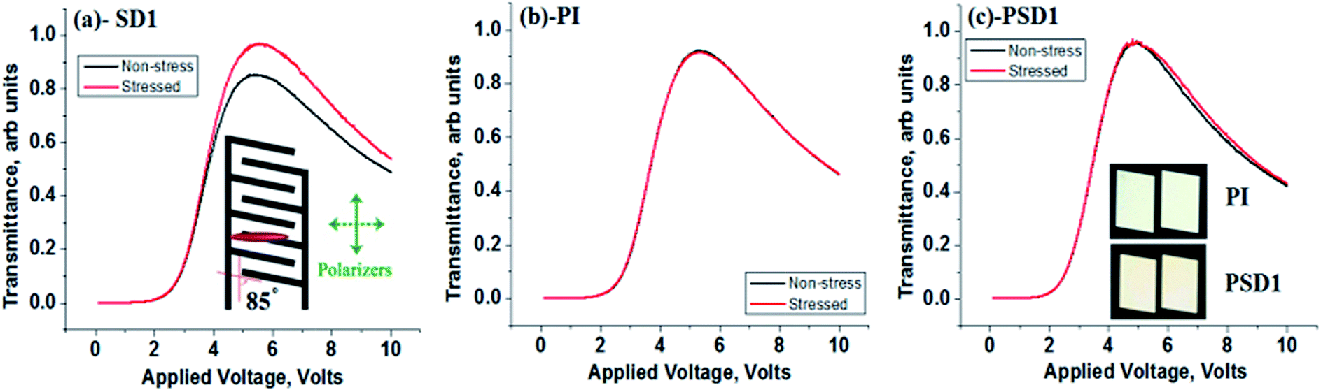 | ||
| Fig. 8 Transmittance versus applied voltage curves for the IPS cells with (a) bare SD1, (b) PI and (c) passivated SD1 filled with LC MDA-4679. The insertion in part (a) show a schematic of the IPS finger electrodes and the alignment direction of LC molecules. The insertion in part (c) shows photos of the pairs of IPS pixels powered by 5 V and viewed between crossed polarizers. The top pair corresponds to rubbed polyimide sample and the bottom pair refers to passivated SD1 sample. In each pair, the left pixel was preliminarily stressed by an electric field of 6 V at 60 Hz for 6 h, while the right pixel remained unstressed. | ||
The hysteresis of the T–V curves was considered to estimate the image sticking (IS), which is a very important electro-optic parameter, especially for high-resolution LCDs, in particular those based on in-plane switching. While the RDC voltage characterizes the electrical contribution to the image retention, the IS parameter gives a measure of its optical manifestation which is actually perceived by the human eye. The IS was measured by the IPS cell with a two-pixel configuration. One of these pixels was stressed by 6 V at 60 Hz for 6 h, whereas no electric field was applied on the second pixel. Afterwards, the T–V curve was measured for the two pixels. The T–V curves for the stressed (red plot) and non-stressed (black plot) pixels are shown in Fig. 8 for pure SD1, PI and passivated SD1. As commonly accepted, the IS parameter was measured as a ratio of the transmittances of stressed and non-stressed pixels for the lower gray scales. The IS vs. applied voltage curves derived from Fig. 8 are shown in Fig. 9. It is obvious that the IS values for SD1 are considerably higher than those for rubbed PI. Passivation of SD1 films makes the IS parameter comparable to that of rubbed PI. Moreover, the samples behave even better at higher applied voltage; whereas the IS parameter for SD1 films grows with the voltage, the IS parameter for passivated SD1 and rubbed PI films drops and approaches 1, which corresponds to the sticking free response (Fig. 8b and c). For example, at 5 V, corresponding to maximal transmittance, the IS parameter is 1.119 for non-passivated SD1 and 1.002 for the RM passivated SD1 films. The latter is practically equal to that obtained for rubbed PI films. To illustrate negligible image sticking in this case, the photographs of the stressed and non-stressed pixels at 5 V for PI and passivated SD1 are shown in the inset to Fig. 8c. No optical contrast between the stressed and unstressed pixels is observed.
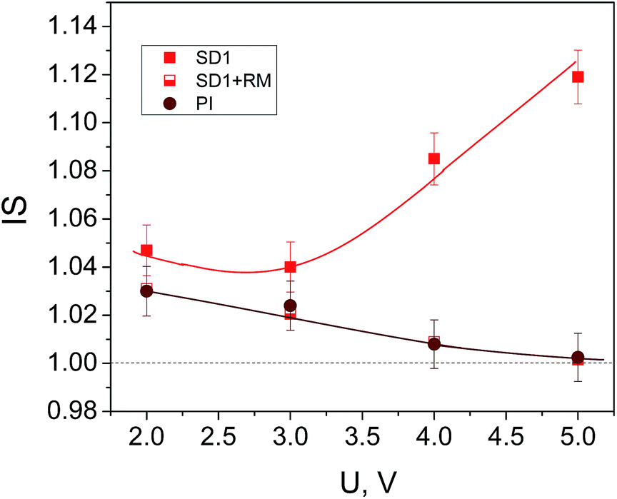 | ||
| Fig. 9 Image sticking (IS) parameter as a function of applied voltage for the IPS cells with pure SD1, passivated SD1 and rubbed PI aligning layers filled with LC MDA-01-4679. | ||
4. Conclusions
The effect of passivating layers of RM on the properties of photoaligning layers of disazo dye SD1 has been comprehensively studied. Using this approach, great improvement of the photo-stability of the LC alignment on the dye films has been achieved. Stabilization effects are observed starting from the RM thickness dRM = 5 nm, which is the minimal thickness of continuous RM films formed on SD1. In order to minimize the undesirable retardation and scattering and optimize the electrical parameters, the thickness of RM films over the dye films is advised to be set at 6–10 nm, i.e., close to the limiting value. Thickening of RM films essentially does not affect the azimuthal anchoring and pre-tilt angle, but leads to increased polar anchoring energy. On the other hand, the passivation drastically improves the electro-optical parameters of SD1 films, such as VHR, RDC voltage and IS parameter, making them practically identical to those of rubbed PI films. The main parameters of the cells with bare SD1, passivated SD1 and rubbed PI aligning layers are compared in Table 1. One can conclude that, based on this approach, many advantages of rubbed PI alignment such as alignment stability and excellent VHR/RDC/IS values can be achieved by keeping the known advantages of photoalignment such as ease of alignment patterning, alignment on curved and mechanically inaccessible surfaces, etc. This combination of properties makes the proposed aligning layers very attractive for modern LC displays and photonic devices. We believe that the applicability of this approach stretches far beyond the class of disazo dyes so that it significantly expands the range of photoaligning materials useful for industrial applications.Acknowledgements
The authors thank to Dr Chung-Yung Lee for fruitful discussions. We thankfully acknowledge the funding supports for partner's State Key Laboratory on Advanced Displays and Optoelectronics Technologies, Hong Kong university of science and technology, Hong Kong. The Hong Kong SAR Research Grants Council grants number 614413 has been gratefully acknowledged.References
- V. G. Chigrinov, Liquid Crystal Devices: Physics and Applications, Artech House, Boston, London, 1999 Search PubMed.
- O. Yaroshchuk and Yu. Reznikov, J. Mater. Chem., 2012, 22, 286–300 RSC.
- B. Chigrinov, E. Prudnikova, V. Kozenkov, H. S. Kwok, H. Akiyama and T. Kawara, Liq. Cryst., 2002, 29, 1321–1327 CrossRef.
- O. Yaroshchuk, J. Ho, V. Chigrinov and H. S. Kwok, Jpn. J. Appl. Phys., 2007, 46(5A), 2995 CrossRef CAS.
- A. Murauski, V. Chigrinov, L. Xihua and H. S. Kwok, Optically rewriteable LC display with a high contrast and long life time, IDW/AD, 2005, p. 131 Search PubMed.
- J. Sun, A. K. Srivastava, W. Zhang, L. Wang, V. G. Chigrinov and H. S. Kwok, Opt. Lett., 2014, 39(21), 6209 CAS.
- E. A. Shteyner, A. K. Srivastava, V. G. Chigrinov, H. S. Kwok and A. D. Afanasyev, Soft Matter, 2013, 9, 5160 RSC.
- H. Takada, H. Akiyama, H. Takatsu, V. Chigrinov, E. Prudnikova, V. Kozenkov and H. S. Kwok, SID'03 Digest, Baltimore, May, 2003, pp. 620–623 Search PubMed.
- K. Hanaoka, Y. Nakanishi, Y. Inoue, S. Tanuma, Y. Koike and K. Okamoto, Society for Information Display Technical Digests, 2004, 35, 1200 CAS.
- S. G. Kim, S. M. Kim, Y. S. Kim, H. K. Lee, S. H. Lee, G.-D. Lee, J.-J. Lyu and K. H. Kim, Appl. Phys. Lett., 2007, 90, 261910 CrossRef.
- Y. J. Lim, I. H. Jeong, H.-S. Kang, S. Kundu, M.-H. Lee and S. H. Lee, Appl. Phys. Express, 2012, 5, 081701 CrossRef.
- V. Finnemeyer, D. Bryant, R. Reich, H. Clark, S. Berry, C. Bozler, O. Yaroshchuk, L. Lu and P. Bos, J. Appl. Phys., 2015, 118, 034501 CrossRef.
- K.-H. Kim, J.-I. Baek, B.-H. Cheong, H.-Y. Choi, S. T. Shin, J. C. Kim and T.-H. Yoon, Appl. Phys. Lett., 2010, 96, 213507 CrossRef.
- S.-W. Oh, J.-H. Park and T.-H. Yoon, Opt. Express, 2015, 23, 1044 CrossRef PubMed.
- Q. Guo, A. K. Srivastava, V. G. Chigrinov and H. S. Kwok, Liq. Cryst., 2014, 41(10), 1465–1472 CrossRef CAS.
- R. A. M. Hikmet and C. de Witz, J. Appl. Phys., 1991, 70, 1265 CrossRef CAS.
- Y.-K. Moon, Y.-J. Lee, S. I. Jo, Y. Kim, J. U. Heo, J.-H. Baek, S.-G. Kang, C.-J. Yu and J.-H. Kim, J. Appl. Phys., 2013, 113, 234504 CrossRef.
- O. Yaroshchuk, V. Kyrychenko, D. Tao, V. Chigrinov, H. S. Kwok, H. Hasebe and H. Takatsu, Appl. Phys. Lett., 2009, 95, 021902 CrossRef.
- N. Kim, H. Lam and T. Kyu, J. Phys. Chem. B, 2010, 114, 16381 CrossRef CAS PubMed.
- O. Yaroshchuk, T. Sergan and J. Kelly, Mol. Cryst. Liq. Cryst., 2001, 367, 143 CrossRef CAS.
- O. Yaroshchuk, L. Dolgov, J. Ho, H. S. Kwok, V. Chigrinov, H. Takatsu and H. Hasebe, Journal of the SID, 2008, 16(9), 933 Search PubMed.
- O. Yaroshchuk, T. Sergan, J. Lindau, S. N. Lee, J. Kelly and L.-C. Chien, J. Chem. Phys., 2001, 114, 5330 CrossRef.
- G. Baur, V. Wittwer and D. W. Berreman, Phys. Lett. A, 1976, 56, 142 CrossRef.
- H. Yokoyama and H. A. van Sprang, J. Appl. Phys., 1985, 57, 4520 CrossRef CAS.
- V. Chigrinov, A. Muravski, H.-S. Kwok, H. Takada, H. Akiyama and H. Takatsu, Phys. Rev. E: Stat., Nonlinear, Soft Matter Phys., 2003, 68, 061702 CrossRef PubMed.
- V. A. Konovalov, A. A. Muravski and S. Y. Yakovenko, SID'00 Digest, vol. 620, 2000 Search PubMed.
- RM data sheet, Merck.
- Y. Inaba, K. Katagiri, H. Inoue, J. Kanbe, S. Yoshihara and S. Iijima, Ferroelectrics, 1988, 85, 255 CrossRef.
- A. L. Alexe-Ionescu, R. Barberi, M. Giocondo, G. Cnossen and T. H. van der Donk, Appl. Phys. Lett., 1995, 66(13), 1701 CrossRef CAS.
- G. Cnossen, F. Lagarde and N. van Aerle, Jpn. J. Appl. Phys., 1997, 36, 1185 CrossRef CAS.
- B. Zhang, F. K. Lee, O. K. C. Tsui and P. Sheng, Phys. Rev. Lett., 2003, 91, 215501 CrossRef PubMed.
- F. S. Yeung, J. Y. Ho, Y. W. Li, F. C. Xie, O. K. Tsui, P. Sheng and H. S. Kwok, Appl. Phys. Lett., 2006, 88, 051910 CrossRef.
| This journal is © The Royal Society of Chemistry 2016 |