
n-Type phosphorus-doped nanocrystalline diamond: electrochemical and in situ Raman spectroelectrochemical study†
Z. Vlčková Živcová*a,
O. Franka,
S. Drijkoningenb,
K. Haenenbc,
V. Mortetde and
L. Kavana
aDepartment of Electrochemical Materials, J. Heyrovsky Institute of Physical Chemistry of the AS CR, v.v.i., Dolejškova 3, 182 23, Prague 8, Czech Republic. E-mail: zuzana.vlckova@jh-inst.cas.cz; Tel: +420 26605 3407
bInstitute for Materials Research (IMO), Hasselt University, Wetenschapspark 1, B-3590 Diepenbeek, Belgium
cIMOMEC, IMEC vzw, Wetenschapspark 1, B-3590 Diepenbeek, Belgium
dInstitute of Physics of the AS CR, v.v.i., Na Slovance 2, 182 21, Prague 8, Czech Republic
eCzech Technical University in Prague, Faculty of Biomedical Engineering, Sítná 3105, 272 01 Kladno, Czech Republic
First published on 18th May 2016
Abstract
Electrochemical and in situ Raman spectroelectrochemical characterization of n-type phosphorus-doped nanocrystalline diamond (P-NCD) is carried out. The P-NCD films are grown by microwave plasma enhanced chemical vapour deposition and doped with phosphorus at a concentration of 10![[thin space (1/6-em)]](https://www.rsc.org/images/entities/char_2009.gif) 000 ppm in the gas phase. Micro-Raman spectroscopy determines the film quality (presence of graphitic or amorphous phases). All electrochemical measurements are performed in aqueous 0.5 M H2SO4 electrolyte solution. Electrochemical impedance spectroscopy (EIS) confirms the n-type conduction of a P-NCD electrode and from the Mott–Schottky plot the donor concentration (ND) of 1.8 × 1018 cm−3 is determined. The in situ Raman spectroelectrochemistry is performed in the potential range from −1.5 to 1.5 V vs. Ag/AgCl using two laser excitations (633 nm and 488 nm). In the case of the as-prepared P-NCD film, the Raman modes belonging to non-diamond (sp2) impurities change their intensities during applied potentials. The intensity of such Raman peaks increases at cathodic potentials, while at anodic potentials they disappear. On the other hand, the intensity and position of the sp3 diamond peak (1334 cm−1) exhibit no spectroelectrochemical changes and the same holds for the photoluminescence peak (at 1.68 eV) assigned to Si-impurities. After several cyclic voltammetry (CV) scans, the electrochemical potential window of a P-NCD electrode increases. This is due to the “electrochemical burning” of impurities at large anodic potentials, which is also confirmed by in situ Raman spectroelectrochemistry. Angle-resolved XPS confirms partial electrochemical oxidation of P-NCD in thin surface layers.
000 ppm in the gas phase. Micro-Raman spectroscopy determines the film quality (presence of graphitic or amorphous phases). All electrochemical measurements are performed in aqueous 0.5 M H2SO4 electrolyte solution. Electrochemical impedance spectroscopy (EIS) confirms the n-type conduction of a P-NCD electrode and from the Mott–Schottky plot the donor concentration (ND) of 1.8 × 1018 cm−3 is determined. The in situ Raman spectroelectrochemistry is performed in the potential range from −1.5 to 1.5 V vs. Ag/AgCl using two laser excitations (633 nm and 488 nm). In the case of the as-prepared P-NCD film, the Raman modes belonging to non-diamond (sp2) impurities change their intensities during applied potentials. The intensity of such Raman peaks increases at cathodic potentials, while at anodic potentials they disappear. On the other hand, the intensity and position of the sp3 diamond peak (1334 cm−1) exhibit no spectroelectrochemical changes and the same holds for the photoluminescence peak (at 1.68 eV) assigned to Si-impurities. After several cyclic voltammetry (CV) scans, the electrochemical potential window of a P-NCD electrode increases. This is due to the “electrochemical burning” of impurities at large anodic potentials, which is also confirmed by in situ Raman spectroelectrochemistry. Angle-resolved XPS confirms partial electrochemical oxidation of P-NCD in thin surface layers.
1. Introduction
In recent years, diamond electrochemistry has been focused on boron doped diamond (BDD) electrodes with p-type conductivity. The electrochemical studies of BDD have dealt with the redox behaviour of diamond electrodes,1–5 the effect of surface termination or modification,3,6–12 the influence of doping level,9,13,14 carbon impurities on the diamond surface,6,15 electrochemical pretreatment effects,16,17 electrochemical oxidation of water,18 the effect of crystal morphology and size,16,19–22 surface doping by hole-accumulation layers23–25 and dye-sensitized photoelectrochemistry.26,27There are only a few studies on highly doped diamonds with n-type conductivity, which is due to problems associated with their preparation. The possible reason may be the difficult incorporation of large atoms (such as phosphorus) into the diamond lattice. P is a known n-type dopant with a high charge carrier activation energy of ∼0.56 eV, leading to relatively resistive films.28 Low conductivity is also caused by partial compensation of P-donors by impurities or lattice defects.29,30 Despite some authors having successfully prepared mono- and polycrystalline phosphorus doped diamond films with donor concentrations above 1018 cm−3,31–35 their electrochemical properties have not yet been studied at the level comparable to BDD. Since n-type diamond is suitable for various applications28 it is crucial to have information about the surface space-charge (depletion) layer and about the structural changes in the presence of the electrolyte solution and applied potential. In situ Raman spectroelectrochemistry combines Raman spectroscopy and electrochemistry, which allows monitoring of structural and electronic (shift of Fermi level) changes of an electrode material as results of the electrochemical potentials applied. The first in situ Raman spectroelectrochemical investigation of diamond in aqueous electrolyte solution was performed on polycrystalline boron doped diamond films in 2013.36 To the best of our knowledge, no comparable study exists on n-doped diamond. Here, we present our initial results acquired on P-doped nanocrystalline diamond (P-NCD).
The P-NCD films were prepared by microwave plasma enhanced chemical vapour deposition (MW PE CVD). The studied P-NCD layers are semiconducting (donor concentration of ca. 1018 cm−3) with a hydrogen terminated surface. The Raman modes of diamond lattice have been found to be invariant to the applied electrochemical potential, whereas the layers on the grain boundaries, which contain disordered carbonaceous phases, are highly sensitive to electrochemical treatment.
2. Experimental
2.1. P-NCD films growth
Nanocrystalline phosphorus doped diamond films were deposited on Si substrate (p-type, 100-oriented) which was cleaned with the standard RCA-1 and RCA-2 cleaning procedures.37 Alternatively, the P-NCD films were also grown on Ti substrate (see ESI, Fig. S1†). The substrates were seeded with an aqueous colloidal suspension of ultradispersed detonation diamond (NanoCarbon Institute Co., Ltd., zeta potential of 45 ± 5 mV, and particles size of 6–7 nm) via drop casting and subsequent spin-drying to enhance nucleation.38 The P-NCD layers were deposited in a 5 kW ASTeX microwave plasma enhanced chemical vapour deposition (MWPECVD) system using a plasma in a gas containing 1% methane and phosphine (PH3) as the carbon and dopant sources, respectively in a concentration (phosphorus/carbon ratio in the gas phase) of 10000 ppm. The carrier gas was hydrogen. The films were deposited at 1800 W and 55 Torr at a substrate temperature of 720 °C ± 50 °C. The film thickness (∼600–700 nm) was monitored by in situ laser reflection interferometry.39 The P-NCD layers were grown with naturally hydrogen terminated surface.
2.2. Methods for P-NCD films characterization
The surface topography of P-NCD layers was characterized using scanning electron microscopy (SEM) with a FEI Quanta 200 FEG-SEM scanning electron microscope at 15 kV. Raman spectra were acquired using 633 nm (1.96 eV) and 488 nm (2.54 eV) laser excitation wavelengths and recorded by a Labram HR spectrometer (Horiba Jobin-Yvon) interfaced to an Olympus microscope (objective 50×). Spot size under a 50× long-working distance objective was ca. 1 μm. The laser power under the objective was kept below 1.1 mW to avoid sample heating. The spectrometer was calibrated by the F1g mode of Si at 520.2 cm−1. The X-ray photoelectron spectroscopy (XPS) spectra were recorded using Omicron Nanotechnology instrument equipped with a monochromatized AlKα source (1486.7 eV) and a hemispherical analyzer operating in constant analyzer energy mode with a multichannel detector. The CasaXPS program was used for spectra analysis. Electrochemical and spectroelectrochemical measurements were performed in 0.5 M H2SO4 (pH 0.6) using a three electrode cell: the P-NCD film served as a working electrode, platinum mesh was a counter electrode and Ag/AgCl electrode (sat. KCl) was a reference. Cyclic voltammetric (CV) measurements were carried out using an AUTOLAB PGSTAT128N potentiostat controlled by GPES4 software. The electrochemical impedance spectra were measured at frequencies from 100 kHz to 0.1 Hz using an AUTOLAB PGSTAT128N potentiostat with the frequency response analyzer (EcoChemie). The measurement was controlled by the FRA software. For in situ Raman measurements, the cell was equipped with a glass optical window and the Raman spectra were excited by the 633 nm or 488 nm laser lines. All electrochemical measurements were carried out in Ar atmosphere.3. Results and discussion
3.1. SEM and Raman spectroscopy
The surface morphology of the prepared P-NCD film deposited on Si was evaluated by scanning electron microscopy (SEM) as shown in Fig. 1. The P-NCD film (thickness and grain size < 1 μm) exhibits well-defined and faceted crystals with preferential crystal orientation (111) and with low degree of twinning.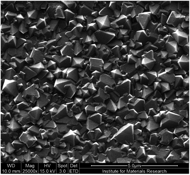 | ||
| Fig. 1 SEM image of the phosphorus doped nanocrystalline diamond (P-NCD) film deposited on Si. | ||
Raman spectra of P-NCD provide useful information about the film quality, especially about non-diamond carbon impurities (sp2 and/or amorphous sp3 carbon). Fig. 2 shows Raman spectra of P-NCD electrode excited by 633 nm (red line) and 488 nm (blue line) laser radiations, respectively. In addition to the narrow zone-center diamond peak at ∼1333 cm−1, the Raman spectrum excited by a laser wavelength of 633 nm contains several more or less resolved peaks. The Raman spectrum excited by a 488 nm laser shows only a few low intensity bands apart from the diamond peak. The sp2 G band is discernible, but its low intensity evidences a good quality of the as-grown P-NCD films. We can only speculate about the origin of the bands visible in the 633 nm spectrum, but given their varying appearance from spot to spot, they could be tentatively assigned to organic compounds adsorbed as contamination from air, and linked to the very active hydrogen terminated surface of the P-NCD. Interestingly, there is no unequivocal evidence of the Raman D (at ∼1330–1350 cm−1) and D′ peaks (1610 cm−1) assignable to graphite-like impurities (sp2 carbon) at the grain boundaries. A significant peak with very high intensity was observed at 2258 cm−1 at the 633 nm excitation (Fig. S1 and S2, see ESI†). This peak (corresponding to photon energy of 1.68 eV) is assigned to photoluminescence, and was observed only in the case of P-NCD film deposited on a Si substrate. We ascribe it to the presence of silicon impurities in the diamond film formed through reaction with the substrate.40 This assignment is confirmed in Fig. S1† showing the Raman spectrum of P-NCD on Ti substrate, where this peak is absent. Due to the small content of substitutionally incorporated phosphorus (ca. 1018 cm−3) the Raman features belonging to P-induced structural defects in the diamond lattice are not distinguished. More specifically, Janssen et al.39 found that, at the growth conditions used here, the P content was about 7.5 × 10¹⁸ P per cm−3 (found by SIMS) to 3.5 × 10¹⁹ P per cm−3 (found by STEM-EDX). Significant fraction of P-atoms was in the bulk of grains, but some P-atoms were at the grain boundaries and/or at the not-substitutional sites in the grains.
 | ||
| Fig. 2 Raman spectra of the phosphorus doped nanocrystalline diamond (P-NCD) deposited on Si substrate excited by 633 nm (red line) and 488 nm (blue line) laser radiations. The spectra are offset for clarity, but the intensity scale is the same. | ||
3.2. Electrochemical characterization
Fig. 3 displays cyclic voltammograms (CV) of hydrogen-terminated P-NCD deposited on Si measured in 0.5 M H2SO4 at a scan rate of 100 mV s−1. In the case of fresh P-NCD electrode (black line), the anodic/cathodic currents start to grow at approximately 0.5 V and −0.8 V vs. Ag/AgCl, respectively. Interestingly, this potential window (≈1.3 V) is quite near the theoretical window of water electrolysis (1.23 V), which indicates surprisingly small overvoltages of both the H2/O2 evolution at our pristine P-NCD electrode. In other words, our electrode obviously contains impurities (such as sp2 carbons) acting as efficient electrocatalyst for water splitting. However, such electrocatalytic impurities are quickly removed by subsequent progressive cycling. This is demonstrated on the cyclic voltammogram of P-NCD electrode after 12 electrochemical cycles (Fig. 3; red line). The “electrochemical cleaning” of P-NCD resembles the one observed in our previous work36 on the polycrystalline boron doped diamond (BDD) films, where the width of the electrochemical potential window analogously scaled with the film quality. The “electrochemical burning” of sp2 carbon at large anodic (2.5 V vs. Ag/AgCl)/cathodic (−2.5 V vs. Ag/AgCl) electrochemical potentials was also confirmed by in situ Raman spectroelectrochemistry (see Section 3.3.). The electrocatalytic function is likely to be associated with the redox processes within surface oxide functionalities at the sp2 carbons in the sample.15 A similar effect has recently been observed in electron emission experiments, where emission from grain boundaries decreased over time, due to irreversible degradation of the surface.41 Changes of the diamond surface after electrochemical cycling at large anodic/cathodic electrochemical potentials were monitored by X-ray photoelectron spectroscopy (XPS) on a fresh as-grown hydrogen terminated P-NCD surface and on the same P-NCD surface after 12 electrochemical cycles (see ESI – Fig. S3, Table S1†). The XPS spectra were recorded at two different emission angles (i) 90° (normal to surface) – detection of deeper layers of the sample, and (ii) 9° – examination of upper layers of the sample. The C1s XPS spectrum of the P-NCD after electrochemical cycling (Fig. S4B and D†), shows that the anodic oxidation of the originally hydrogen-terminated electrode surface (Fig. S4A and C†) leads to formation of the surface oxygen-containing functional groups (hydroxyl or carbonyl). The deconvolution of the main C1s peak (ca. 285 eV) in the case of P-NCD after electrochemical cycling showed according to the position of individual components presence of C–O (ca. 286 eV) and C![[double bond, length as m-dash]](https://www.rsc.org/images/entities/char_e001.gif) O (ca. 288 eV) bonds on the diamond surface.42,43 The angle-resolved XPS spectra confirm that P-NCD is oxidized in thin surface layer only.
O (ca. 288 eV) bonds on the diamond surface.42,43 The angle-resolved XPS spectra confirm that P-NCD is oxidized in thin surface layer only.
 | ||
| Fig. 3 Cyclic voltammograms of phosphorus doped nanocrystalline diamond (fresh P-NCD electrode – black line, P-NCD electrode after electrochemical cycling – red line). Electrolyte solution; aqueous 0.5 M H2SO4. Scan rate; 100 mV s−1. | ||
To further explore the doping mechanism in our P-NCD electrode, electrochemical impedance spectra were measured. Fig. 4 shows the equivalent circuit used for fitting the experimental data which takes into account the diffusion phenomena.25,44 This circuit consists of the ohmic resistance (Rs) of the electrolyte solution, electrodes, contacts etc. in series with the parallel combination of the space charge capacitance (P-NCD/electrolyte interface) represented by a constant phase element (CPE) and its associated resistance (R1) in series with diffusion impedance (Zw), the so-called Warburg element.
 | ||
| Fig. 4 Equivalent circuit used to fit the electrochemical impedance spectra for nanocrystalline phosphorus doped diamond (P-NCD) films; Rs is ohmic serial resistance, CPE is constant phase element, R1 is the associated charge transfer resistance and Zw is the Warburg element. | ||
Several other types of equivalent circuits were also tested for the fitting of our impedance spectra. Similarly to the previous work on polycrystalline boron doped diamond films,45 the circuit with CPE and Warburg impedance (Fig. 4) provided the best fit to experimental spectra for P-NCD.
The impedance of a CPE equals:
| ZCPE = B(iω)−β | (1) |
The capacitance, C is obtained from ZCPE as follows:
 | (2) |
An obvious advantage of this evaluation protocol is that it removes the virtual ‘frequency dispersion’ of Mott–Schottky plots.48–50 This dispersion was often pronounced also on the diamond electrodes.8,25,25,51 For the equivalent circuit shown in Fig. 4, the capacitance C is assumed to be equal to the capacitance of the space charge layer in the diamond electrode, that is C = Csc. In the potential range of water stability, the values of R1 are very high (of the order of 1012 Ω), therefore this resistance can be neglected in the equivalent circuit in Fig. 4 (ref. 52) and the response is almost perfectly capacitive. However, at more positive potentials the resistances of R1 decrease to values up to ca. 105 Ω. Such smaller values of R1, observed at a potential close to the depletion regime, can indicate a faradaic leakage at the interface.
Fig. 5 shows the Mott–Schottky plot for P-NCD after electrochemical cycling. The plot was linear in the indicated potential range, while over the wider potential range (from 1 V to −1 V vs. Ag/AgCl) the plot showed a typical S-shape caused by the heterogeneous character of the polycrystalline interface.44,53,53–57 The positive slope of the Mott–Schottky plot confirms the n-type conductivity of P-NCD films. This finding is not trivial, due to complicated phosphorus-chemistry in P-NCD (with compensated or non-ionized donors, non-substitutional sites, grain boundaries, etc.), discussed above.58 The Mott–Schottky equation was used to calculate the donor concentration ND:
 | (3) |
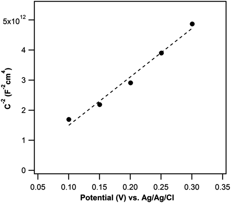 | ||
| Fig. 5 Mott–Schottky plot for the phosphorus doped nanocrystalline diamond (P-NCD) film deposited on Si substrate. The donor concentration (ND) was determined from the slope. This fit was carried our using the equivalent circuit in depicted Fig. 4. | ||
The donor concentration (ND) of P-NCD film determined from the Mott–Schottky plot was 1.8 × 1018 cm−3. Based on the previously published work of Janssen et al.39 we expect a P-content in the sample of about 1019 P per cm−3 (analyzed by SIMS and STEM-EDX). The smaller ND found in the current work indicates that not all of P atoms contribute to the electron conductivity. In other words, our impedance spectra confirm that significant proportions of P-atoms are localized at inactive sites in the lattice, and they are not involved in the n-doping, as discussed above. We should note that, due to the resistivity of the films, Hall measurements provided inconclusive results on these samples. In turn, our EIS data clearly confirm that these films are n-type, as expected.
3.3. In situ Raman spectroelectrochemical characterization
Fig. 6 shows a set of Raman spectra of our fresh P-NCD electrode measured in cathodic (gray lines) and anodic (black lines) potentials sweep and excited by the red laser 633 nm (Fig. 6 top) or blue laser 488 nm (Fig. 6 bottom). The electrochemical measurements have been performed in aqueous electrolyte solution (0.5 M H2SO4) in the potential range of −1.5 to 1.5 V vs. Ag/AgCl. In all spectra the mode belonging to the zone-center sp3 phonon (at 1333 cm−1) exhibited no changes with the applied potential neither in anodic nor cathodic directions. This indicates a high stability of the bulk diamond lattice with incorporated phosphorus, as well as no influence of the Fermi level shifts on the Raman spectra in the applied potential range. This observation is in line with the previous in situ spectroelectrochemical works both on polycrystalline and single-crystalline B-doped diamond films.36,59 The majority of spectroelectrochemical changes occur between 1500 and 1700 cm−1, i.e. in the spectral region where bands belonging to the G mode of sp2-carbon appear, with their particular frequencies being dependent on the sp2/sp3 content.60 At the 633 nm excitation, a multi-component structure with at least two sub-peaks centered at 1580 and 1610 cm−1 appears at the cathodic bias. It is tempting to assign the peak at 1610 cm−1 to the sp2 disorder-induced D′ band, however, the absence of the main defect-related D band (at ∼1330 cm−1) makes such an assignment improbable. A G band belonging to a phase with more than 20% of sp3 bonds, which is not accompanied by the D band,60 might be a more plausible explanation. It is worth noting that the bands appear at the strongest intensity in the 1st spectroelectrochemical cycle, while in the subsequent ones, their intensity drops. The experiment at the 488 nm excitation exhibits a similar behaviour: a complex feature at ∼1600 cm−1, though with different relative intensities of its components, emerges at negative potentials and vanishes again at positive ones. During progressive cycling, the total intensity of this feature diminishes even at cathodic potentials (Fig. 6 bottom). These observed variations of the spectral features belonging to the non-diamond phases, probably located at the P-NCD grain boundaries were also observed in the case of in situ Raman spectroelectrochemical measurements of boron doped diamond (BDD).36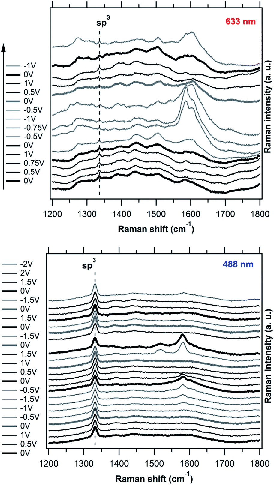 | ||
| Fig. 6 In situ Raman spectroelectrochemical data of the phosphorus doped nanocrystalline diamond (P-NCD) electrode measured at cathodic (gray line) and anodic (black line) potentials. The spectra are excited by 633 nm (top) and 488 nm (bottom) laser radiations and offset for clarity. The electrolyte solution was aqueous 0.5 M H2SO4. The electrode potentials are referred against the Ag/AgCl electrode. The measurement direction was from bottom to top. | ||
To test the sample stability against laser light, we made reference experiments both in air and in aqueous electrolyte solution 0.5 M H2SO4, with samples continuously irradiated by the laser for 40 minutes and Raman spectra acquisition every 5 minutes (see ESI, Fig. S5†). No appearance/disappearance of Raman features has been observed. With respect to the used acquisition time during spectroelectrochemical experiments (120 s), the possibility of surface alteration by the laser can be ruled out in the spectra presented in Fig. 6. Also the control cyclic voltammogram (see ESI, Fig. S6†) of the final sample after in situ Raman spectroelectrochemistry confirms that the laser-light treatment has no marked influence on the electrochemical properties of these electrodes.
The variation of intensity of the new bands can be explained by alteration of the diamond surface by electrochemical redox reactions. Such a scenario is in agreement with the results of the cyclic voltammetry on the as-prepared fresh P-NCD vs. P-NCD after electrochemical treatment at high potentials, where we proposed that the water decomposition currents drop as a result of the gradual removal of non-diamond carbon impurities by anodic oxidation. We can assume that the networks of imperfectly bonded atoms (disordered mixture of sp2 and sp3 hybridized atoms) at the surface are disrupted by hydrogen-involving reaction at negative potentials, followed by an oxidative “electrochemical burning” of the exposed carbon atoms in the anodic regime. Due to the very small amount of sp2 carbon in the as-prepared fresh P-NCD and the absence of the D band during the spectroelectrochemical experiment, an evolution via the delamination of shallow sp2 networks as in ref. 36 can be excluded. On the other hand, the effect of successful cleaning of the diamond surface is clearly demonstrated by the changes of the Raman spectra in addition to electrochemical data.
4. Conclusions
Phosphorus doped nanocrystalline diamond (P-NCD) films were deposited on Si or Ti substrates by microwave plasma enhanced chemical vapour deposition (MW PE CVD) and characterized by electrochemical, XPS and Raman spectroscopic techniques. The P-NCD films show well-defined and faceted crystals with low degree of twinning. The equivalent circuit with CPE and Warburg impedance provided the best fit to the electrochemical impedance spectra for P-NCD. From the Mott–Schottky plot n-type doping of the P-NCD film was successfully determined with a donor concentration (ND) of 1.8 × 1018 cm−3. The Raman spectroscopy shows only a minor contribution from sp2 carbonaceous impurities. On the other hand, the in situ Raman spectroelectrochemistry demonstrates changes in the topmost layers on the P-NCD grain boundaries. The diamond (sp3 carbon) Raman features of P-NCD as well as the photoluminescence peak, assigned to Si-impurities, are invariant to electrochemical charging. The sequential electrochemical cycling causes first the appearance of Raman modes originating probably in defective sp3 lattice on the grain surfaces, followed by their continuous removal in the anodic regime by oxidation. The intensities of these bands continuously decrease with progressing electrochemical cycling, evidencing the electrochemically-driven cleaning of the P-NCD surface.Acknowledgements
This work was supported by the Grant Agency of the Czech Republic (contract No. 13-31783S), the Research Foundation Flanders (FWO) (G.0456.12) and the J. E. Purkyně fellowship awarded to V. Mortet by Academy of Sciences of the Czech Republic.Notes and references
- N. Vinokur, B. Miller and Y. Avyigal, et al., J. Electrochem. Soc., 1996, 143, L238–L240 CrossRef CAS.
- M. C. Granger, M. Witek, J. S. Xu, J. Wang and M. Hupert, Anal. Chem., 2000, 72, 3793 CrossRef CAS PubMed.
- I. Yagi, H. Notsu, T. Kondo, D. A. Tryk and A. Fujishima, J. Electroanal. Chem., 1999, 473, 173 CrossRef CAS.
- K. B. Holt, C. Ziegler, J. Zang, J. Hu and J. S. Foord, J. Phys. Chem. C, 2009, 113, 2761 CAS.
- N. Yang, J. S. Foord and X. Jiang, Carbon, 2016, 99, 90 CrossRef CAS.
- H. B. Martin, A. Argoitia, J. C. Angus and U. Landau, J. Electrochem. Soc., 1999, 146, 2959 CrossRef CAS.
- D. A. Tryk, K. Tsunozaki, T. N. Rao and A. Fujishima, Diamond Relat. Mater., 2001, 10, 1804 CrossRef CAS.
- G. Pastor-Moreno and D. J. Riley, Electrochim. Acta, 2002, 47, 2589 CrossRef CAS.
- M. N. Latto, G. Pastor-Moreno and D. J. Riley, Electroanalysis, 2004, 16, 434 CrossRef CAS.
- J. S. Foord, W. Hao and S. Hurst, Diamond Relat. Mater., 2007, 16, 877 CrossRef CAS.
- P. Actis, A. Denoyelle, R. Boukherroub and S. Szunerits, Electrochem. Commun., 2008, 10, 402 CrossRef CAS.
- F. B. Liu, J. D. Wang, B. Liu, X. M. Li and D. R. Chen, Diamond Relat. Mater., 2007, 16, 454 CrossRef CAS.
- T. Watanabe, T. K. Shimizu, Y. Tateyama, Y. Kim, M. Kawai and Y. Einaga, Diamond Relat. Mater., 2010, 19, 772 CrossRef CAS.
- A. F. Azevedo, M. R. Baldan and N. G. Ferreira, Int. J. Electrochem., 2012, 2012, 1 CrossRef.
- J. Foord and J. P. Hu, Phys. Status Solidi A, 2006, 203, 3121 CrossRef CAS.
- T. Yano, E. Popa, D. A. Tryk, K. Hashimoto and A. Fujishima, J. Electrochem. Soc., 1999, 146, 1081 CrossRef CAS.
- M. A. Kulandainathan, C. Hall, D. Wolverson, J. S. Foord, S. M. MacDonald and F. Marken, J. Electroanal. Chem., 2007, 606, 150 CrossRef CAS.
- P. A. Michaud, M. Panizza, L. Ouattara, T. Diaco, G. Foti and C. Comninellis, J. Appl. Electrochem., 2003, 33, 151 CrossRef CAS.
- Y. Pleskov, Y. Evstefeeva, M. D. Krotova, V. G. Ralchenko, I. I. Vlasov, E. N. Loubnin and A. V. Khomich, J. Appl. Electrochem., 2003, 33, 909 CrossRef CAS.
- Y. Pleskov, Y. Evstefeeva, M. D. Krotova, V. P. Varnin and I. G. Teremetskaya, J. Electroanal. Chem., 2006, 595, 168 CrossRef CAS.
- Y. Einaga, G. S. Kim, S. G. Park and A. Fujishima, Diamond Relat. Mater., 2001, 10, 306 CrossRef CAS.
- S. Wang, V. M. Swope, J. E. Butler, T. Feygelson and G. M. Swain, Diamond Relat. Mater., 2009, 18, 669 CrossRef CAS.
- P. Strobel, M. Riedel, J. Ristein and L. Ley, Nature, 2004, 430, 439 CrossRef CAS PubMed.
- C. E. Nebel, B. Rezek, D. Shin and H. Watanabe, Phys. Status Solidi B, 2006, 203, 3273 CrossRef CAS.
- J. A. Garrido, S. Nowy, A. Hartl and M. Stutzmann, Langmuir, 2008, 24, 3897 CrossRef CAS PubMed.
- H. Krysova, Z. Vlckova-Zivcova, J. Barton, V. Petrak, M. Nesladek, P. Cigler and L. Kavan, Phys. Chem. Chem. Phys., 2015, 17, 1165 RSC.
- H. Krysova, L. Kavan, Z. V. Zivcova, W. S. Yeap, P. Verstappen, W. Maes, K. Haenen, F. Gao and C. E. Nebel, RSC Adv., 2015, 5, 81069 RSC.
- M. Nesladek, Semicond. Sci. Technol., 2005, 20, R19 CrossRef CAS.
- N. Casanova, A. Tajani, E. Gheeraert, E. Bustarret, J. A. Garrido, C. E. Nebel and M. Stutzmann, Diamond Relat. Mater., 2002, 11, 328 CrossRef CAS.
- S. Koizumi, M. Kamo, Y. Sato, S. Mita, A. Sawabe, A. Reznik, C. Uzan-Saguy and R. Kalish, Diamond Relat. Mater., 1998, 7, 540 CrossRef CAS.
- S. Koizumi, M. Kamo, Y. Sato, H. Ozaki and T. Inzuka, Appl. Phys. Lett., 1997, 71, 1065 CrossRef CAS.
- E. Gheeraert, S. Koizumi, T. Teraji and H. Kanda, Solid State Commun., 2000, 113, 577 CrossRef CAS.
- H. Kato, D. Takeuchi, M. Ogura, T. Yamada, M. Kataoka, Y. Kimura, S. Sobue, C. E. Nebel and S. Yamasaki, Diamond Relat. Mater., 2016, 63, 165 Search PubMed.
- K. Haenen, A. Lazea, J. Barjon, J. D'Haen, N. Habka, T. Teraji, S. Koizumi and V. Mortet, J. Phys.: Condens. Matter, 2009, 21, 364204 CrossRef PubMed.
- T. Yamada, K. Okano, H. Yamaguchi, H. Kato, S. Shikata and C. E. Nebel, Appl. Phys. Lett., 2006, 88, 212114 CrossRef.
- Z. V. Živcová, O. Frank, V. Petrák, H. Tarábková, J. Vacík, M. Nesládek and L. Kavan, Electrochim. Acta, 2013, 87, 518 CrossRef.
- W. A. Kern and D. A. Puotinen, RCA Rev., 1970, 31, 187 CAS.
- O. A. Williams, O. Douhéret, M. Daenen, K. Haenen, E. Osawa and M. Takahashi, Chem. Phys. Lett., 2007, 445, 255 CrossRef CAS.
- W. Janssen, S. Turner, G. Sakr, F. Jomard, J. Barjon, G. Degutis, Y. G. Lu, J. D'Haen, A. Hardy, M. V. Bael, J. Verbeeck, G. V. Tendeloo and K. Haenen, Phys. Status Solidi RRL, 2014, 8, 705 CrossRef CAS.
- M. Mermoux, B. Marcus, L. Abello, N. Rosman and G. Lucazeau, J. Raman Spectrosc., 2003, 34, 505 CrossRef CAS.
- R. L. Harniman, O. J. L. Fox, W. Janssen, S. Drijkoningen, K. Haenen and P. W. May, Carbon, 2015, 94, 386 CrossRef CAS.
- S. Torrengo, R. Canteri, R. DellGÇÖAnna, L. Minati, A. Pasquarelli and G. Speranza, Appl. Surf. Sci., 2013, 276, 101 CrossRef CAS.
- J. Hernando, S. Q. Lud, P. Bruno, D. M. Gruen, M. Stutzmann and J. A. Garrido, Electrochim. Acta, 2009, 54, 1909 CrossRef CAS.
- M. R. Baldan, A. F. Azevedo, A. B. Couto and N. G. Ferreira, J. Phys. Chem. Solids, 2013, 74, 1830 CrossRef CAS.
- Z. V. Živcová, V. Petrák, O. Frank and L. Kavan, Diamond Relat. Mater., 2015, 55, 70 CrossRef.
- G. J. Brug, A. L. G. Van Den Eeden, M. Sluyters-Rehbach and J. H. Sluyters, J. Electroanal. Chem., 1984, 176, 275 CrossRef CAS.
- P. Zoltowski, J. Electroanal. Chem., 1998, 443, 149 CrossRef CAS.
- L. Kavan, M. Zukalova, O. Vik and D. Havlicek, ChemPhysChem, 2014, 15, 1056 CrossRef CAS PubMed.
- L. Kavan, N. Tetreault, T. Moehl and M. Grätzel, J. Phys. Chem. C, 2014, 118, 16408 CAS.
- M. Zukalova, M. Bousa, Z. Bastl, I. Jirka and L. Kavan, J. Phys. Chem. C, 2014, 118, 25970 CAS.
- L. Boonma, T. Yano, D. A. Tryk, K. Hashimoto and A. Fujishima, J. Electrochem. Soc., 1997, 144, L142–L145 CrossRef CAS.
- A. Denisenko, C. Pietzka, A. Romanyuk, H. El-Hajj and E. Kohn, J. Appl. Phys., 2008, 103, 14904 CrossRef.
- P. Actis, A. Denoyelle, R. Boukherroub and S. Szunerits, Electrochem. Commun., 2008, 10, 402 CrossRef CAS.
- A. F. Azevedo, M. R. Baldan and N. G. Ferreira, J. Phys. Chem. Solids, 2013, 74, 599 CrossRef CAS.
- A. F. Azevedo, F. A. Souza, P. Hammer, M. R. Baldan and N. G. Ferreira, J. Nanopart. Res., 2011, 13, 6133 CrossRef CAS.
- N. Simon, H. Girard, D. Ballutaud, S. Ghodbane, A. Deneuville, M. Herlem and A. Etcheberry, Diamond Relat. Mater., 2005, 14, 1179 CrossRef CAS.
- H. Girard, N. Simon, D. Ballutaud, M. Herlem and A. Etcheberry, Diamond Relat. Mater., 2007, 16, 316 CrossRef CAS.
- M. A. Pinault-Thaury, I. Stenger, F. Jomard, J. Chevallier, J. Barjon, A. Traore, D. Eon and J. Pernot, Phys. Status Solidi A, 2015, 212, 2454 CrossRef CAS.
- L. Kavan, Z. Vlckova Zivcova, V. Petrak, O. Frank, P. Janda, H. Tarabkova, M. Nesladek and V. Mortet, Electrochim. Acta, 2015, 179, 626 CrossRef CAS.
- A. C. Ferrari and J. Robertson, Phys. Rev. B: Condens. Matter Mater. Phys., 2000, 61, 14095 CrossRef CAS.
Footnote |
| † Electronic supplementary information (ESI) available. See DOI: 10.1039/c6ra05217g |
| This journal is © The Royal Society of Chemistry 2016 |