R. Paul*a,
R. N. Gayenb,
S. Biswasc,
S. Venkataprasad Bhat*d and
R. Bhuniaa
aDepartment of Instrumentation Science, Jadavpur University, Kolkata 700032, India. E-mail: rajiv2008juniv@gmail.com; paul24@purdue.edu
bDepartment of Physics, Presidency University, Kolkata 700073, India
cDepartment of Chemistry, Jadavpur University, Kolkata 700032, India
dSRM Research Institute & Department of Physics and Nanotechnology, SRM University, Chennai 603203, India. E-mail: venkataprasad.b@res.srmuniv.ac.in
First published on 22nd June 2016
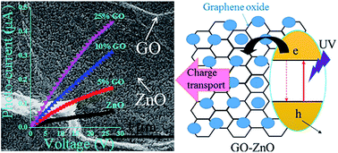
All solution processed transparent thin films of graphene oxide (GO) and zinc oxide (ZnO) in different compositions prepared by a simple two-step chemical synthesis method have been studied for their UV detection properties. The preparation of GO through oxidation of graphite flakes is followed by sol–gel spin coating deposition of the GO–ZnO composite films on glass substrates. The surface morphology, microstructure and composition of the samples have been studied to confirm the formation of composite thin films comprising wurtzite-ZnO nanocrystallites and GO flakes. Optical studies demonstrate that both the transparency and optical band gap of the samples as estimated from wavelength dependent transmittance curves decrease with the increase of GO content in the films, while the charge carrier concentration increases by 5 fold. The in-plane current–voltage (I–V) measurements with two silver electrodes on the GO–ZnO film show a significant enhancement of the photosensitivity in comparison to ZnO films when they are exposed to UV light of different intensities. The response time (t90-response) is nearly three times smaller for GO–ZnO composite films as compared to that of pure ZnO. This improvement is attributed to the defect state modulation and carrier density improvement of the thin films with incorporation of GO, which is encouraging to propel optical, electrical and hence optoelectronics applicability of ZnO composite based transparent devices.
In recent times, several efforts have been made to solve this issue by combining ZnO with other functional materials like graphene, reduced graphene oxide (rGO) or GO.5,15–17 The working mechanism lays behind the controlling of defect states, carrier concentration, carrier mobility and lifetime which are golden parameters in manipulating the photoconductivity of ZnO.18 Recently researchers have tried to modify the spectral response of ZnO so that it becomes more efficient in the visible spectral regime by altering its defect states.19,20 The composite structure formation of ZnO with graphene or graphene oxide is a novel, cost effective and efficient approach to control the morphology, surface defect states, band gap and photoresponse of ZnO nanocrystals.20–22 Moreover, graphene-semiconductor hybrid/composite materials have been identified as suitable candidates for various photonic and optoelectronic applications like photovoltaic cells, optical filters, photodetectors and ultrafast lasers.23 This is due to the excellent electronic properties of graphene and its prominent capability to store and shuttle photogenerated electrons from the band gap excitation of semiconductors upon light irradiation.24
Graphene–ZnO, rGO–ZnO or GO–ZnO hybrid structures are generally prepared by two methods. In first method, ZnO with required morphology is synthesized and then it is bonded to the surface of graphene or rGO. This is performed mainly by epitaxial growth, chemical deposition or self-assembly technique.25,26 In the other technique, GO is used as the precursor and the nucleation of ZnO occurs in presence of GO where GO is reduced automatically in a non-toxic way to rGO which inhibits the photogenerated carriers from recombination and transports them between electrodes.27 This is cost effective and easier process to control the morphology, surface defect states and hence the optoelectronic properties of ZnO. Presence of GO, may hinder the preferential c-axis growth of ZnO because of the interaction between the O-groups of GO and Zn2+ ions.27 Pan et al. have reported that, with the variation of the added amount of GO (upto 10 wt%) the ZnO morphology changes from a 1D prismatic rod with a pointed tip to a hexagonal tube architecture with a hollow interior and flattened tip, while GO is converted to reduced GO.27 Here the GO sheets play a critical role by tuning the morphology of ZnO and creating oxygen vacancies in the ZnO. These oxygen vacancies are favourable for modulating opto-electronic properties in ZnO. Therefore, GO addition may promote the opto-electronic properties and conductivity of GO–ZnO composite materials through defect manipulation and engineering. Hence it is important to perform systematic study for understanding the modulating effect in such composites.
Chang et al. have demonstrated the enhanced UV photoresponsivity for their ZnO–SWNTs hybrid thin films compared to that of pure ZnO films.28 This improvement was attributed to rapid transportation of UV excited electron–hole (e/h) pairs by conductive SWCNTs. Concerning the effects of graphite allotrope in UV photoresponsivity, in another work, the hybrid photodetector based on polymer–ZnO quantum dots (QDs)–graphene layer shows an amazing photoresponsivity.29 More recently, it is shown that significant improvement of UV photodetection performance of integrated ZnO–rGO composite films can be attained through synergetic effects of rGO in electron/hole recombination inhibition and providing an easy passage way for photogenerated carriers.29 Therefore, in order to obtain rGO–ZnO nanocomposite having such synergistic effect, a good interfacial combination between ZnO and rGO is required to promote the charge transfer between ZnO and rGO. However, very few systematic studies on carbon–ZnO hybrid structure (in a layer by layer system) or composite thin-film synthesized through sonochemical technique for UV detection are reported which brings forward the motivation behind this work.5,30 Safa et al. synthesized rGO–ZnO composite with maximum 7.5 wt% rGO in ZnO by a solution process followed by reduction using thermal annealing in nitrogen.5,30 Graphene flakes or rGO however are difficult to mix with ZnO uniformly due to their hydrophobic nature. Hence it remains as a challenge to make uniform composite films based on ZnO and rGO or graphene. But GO being hydrophilic in nature for its available functional groups, is easier to incorporate in ZnO matrix as compared to rGO or graphene. Hence it would be easier to synthesis good quality of composite thin films using GO and ZnO in a simple solution processing technique. A systematic study of the effect of GO addition on the UV detection properties of ZnO in such composite films has yet not been reported. Moreover, it is necessary to optimize the simple synthesis procedure like sol–gel spin coating to fabricate smart composite materials like GO–ZnO as promising transparent UV detector that certainly meets the requirement of cost effective green technology.
Here we report the synthesis and characterization of transparent GO–ZnO composite thin films produced through cost effective and two step all solution processed coating on glass with different amount of GO systematically, demonstrating the modulation of UV photosensitivity. We have also demonstrated the modulation of the generation and transport of charge careers through GO incorporation and reduction into ZnO.
The mixed solutions containing 0%, 5%, 10% and 25% GO (v/v) were spin-coated onto clean glass substrate to obtain GO–ZnO nanocomposite thin films. The substrate was set to rotate at 3000 rpm for 30 s using a programmable spin coater when 10 drops of the solution was drop casted onto it. Then the substrate having a thin uniform layer of solution was dried in an air oven at 120 °C for 10 min. The coating and drying process was repeated for 6 times to get the required thickness with good uniformity. Then the films were annealed finally at 400 °C in an air oven.
Photoluminescence measurement was carried out using a 300 W Xe arc lamp as the emission source, Hamamatsu photomultiplier with 3/4 meter monochromator (Oriel Instruments, Model no. 77200) as the detector. Excitation was varied with another 3/4 meter monochromator (Oriel Instruments, model no 77200). An optical chopper with controller (SR 540, Standford Research Systems) and a lock-in-amplifier (SR 530, Standford Research System) were used at the output for minimizing the noise for measuring the output signal. The lock-in-amplifier along with both the detectors and excitation monochromators were monitored with remote control software. The spectra were digitized and collected by a computer. The detection range could be varied from 200 nm to 2000 nm by changing the optical grating in the detector monochromator. All the photoluminescence measurements were recorded at 300 K with 250 nm excitation for detecting the PL peaks in the range 300–700 nm. For I–V characterization pure silver (Ag) dots were deposited on top of all the thin films by high vacuum thermal evaporation system with proper masking under a vacuum of base pressure better than 10−5 Pa. The thickness and cross-sectional area of Ag top contacts were ∼150 nm and 0.78 × 10⁻² cm−2, respectively. The in-plane I–V characteristics under UV illumination of fixed wavelength 374 nm with different power densities (150 and 750 μW cm−2) of UV illumination were measured by a set-up comprising of constant voltage source and pico-ammeter. The photoresponsivity characterizations were performed at similar illumination of 750 μW cm−2 and by using 374 nm UV excitation from Xe arc lamp at 25 V. A Keithley 2420 sourcemeter was interfaced with computer through LabVIEW program for this purpose.
Fig. 1 represents the FESEM images of ZnO films with different amount of GO incorporated. Fig. 1(a) represents the surface morphology of pure ZnO film without any GO content whereas Fig. 1(b)–(d) show the ZnO films with incorporation of 5%, 10% and 25% GO. The ZnO thin film comprises of uniformly distributed nanocrystallites which are compact in nature. The morphology variation with increasing amount of GO incorporation is evident from the FESEM micrographs. Inset of Fig. 1(c) shows a representative TEM image of 10% GO–ZnO composite film with GO flake and ZnO nanoparticles. Flakes of GO is observed in 25% GO film (Fig. 1(d)) and the inset of Fig. 1(d) shows the cross-sectional SEM image of composite film with 25% GO. Clearly the graphene layers are incorporated into ZnO film.
![]() | ||
Fig. 1 FESEM images of thin films of (a) pure ZnO (b) 5% GO–ZnO (c) 10% GO–ZnO (inset: TEM image) and (d) 25% GO–ZnO (inset shows cross-section of the composite layer). |
To estimate the chemical compositions of the films EDAX measurements are performed. Fig. 2(a) shows representative EDAX spectra of 0%, 5% and 25% GO films. Beside the peaks for Zn and O, presence of other peaks like Si, Al, Na, Sb and Ca, for all the samples, are due to the glass substrate used. Presence of small C peak for GO–ZnO composite films confirms the incorporation of graphene oxide in ZnO films. The amount of carbon (C) content in 5%, 10% and 25% GO–ZnO films are 4.1, 9.2 and 16.4% (at) respectively as shown in Table 1. Fig. 2(b) indicates the variation of C and O content in GO–ZnO composite films.
Sample | C amount (at%) | Crystallite size (nm) | Band gap (eV) | ε∞ | ωp × 1014 (S−1) | N × 1019 (cm−3) | t90-Response (s) | t90-Recovery (s) | Photoresponsivity, R (A W−1) |
---|---|---|---|---|---|---|---|---|---|
ZnO | 0 | 27.7 | 3.27 | 3.45 | 2.15 | 0.63 | 124.63 | 95.84 | 0.005 |
5% GO–ZnO | 4.1 | 24.2 | 3.23 | 3.40 | 4.35 | 2.53 | 56.65 | 65.47 | 0.261 |
10% GO–ZnO | 9.2 | 22.6 | 3.20 | 3.29 | 4.83 | 3.03 | 41.94 | 51.63 | 0.493 |
25% GO–ZnO | 16.4 | 21.3 | 3.17 | 3.10 | 5.19 | 3.30 | 36.03 | 44.57 | 0.827 |
XRD patterns of pure GO, pure ZnO and GO–ZnO composite films are shown in Fig. 3(a). XRD pattern for ZnO film having no GO content shows diffraction peaks due to reflections from (100), (002), (101), (102), (110), (103) and (112) planes that matches very well with the standard data for wurtzite structure of ZnO (JCPDS 36-1451). All the GO–ZnO composite films with different GO incorporation show the same diffraction peaks as pure ZnO which demonstrates that the presence of GO does not affect the crystallinity or the preferred orientation of ZnO. The absence of the GO peak suggests the complete exfoliation and dispersion of GO due to incorporation into the ZnO.32 The XRD pattern of GO has a strong diffraction peak at 2θ ∼ 9.6° due to reflection from (001) plane of graphene oxide33 which is absent in case of GO–ZnO composite films mainly due to low diffraction intensity of graphene oxide in dispersed state.16 Efficient dispersion of GO during ultrasonication reduces the diffraction intensity of GO in ZnO.
Modulation of lattice constants (a and c) of h-ZnO for different films with GO content are evaluated using following equation for hexagonal space lattice:
![]() | (1) |
The lattice constants as evaluated for the ZnO from eqn (1) are a ∼0.323 nm and c ∼ 0.518 nm that remained invariant for the GO–ZnO nanocomposite thin films. As the lattice constants remain unchanged with the increased GO content in the composites, the possibility of C atom incorporation in the ZnO host matrix by replacing Zn or O is negligible. Although the peak positions of the reflections from hexagonal ZnO lattice is remained same for the GO–ZnO nanocomposites, the slight broadening of the XRD peak indicates the decrease in crystallite size of ZnO nanoparticles. The average crystallite size (D) was extracted from the XRD pattern using Scherrer relation:34
D = Kλ/β![]() ![]() | (2) |
Raman spectroscopy is non-destructive technique to investigate the bonding environment and defect related disorder, especially in carbon based materials. Fig. 4 shows the Raman spectra of ZnO, GO and two representative GO–ZnO composite films with 5% and 25% GO. The only peak at 438 cm−1 for ZnO thin film arises due to E2 (high) vibrational mode which is characteristics of wurtzite phase of ZnO.37 Two strong peaks for GO at 1360 cm−1 and 1599 cm−1 are assigned as D-band and G-band, respectively. The D-band is a measure of defects and disorders present in the materials whereas the G-band originates due to E2g symmetric stretching of sp2 hybridized CC bond.38,39 The Raman spectra of ZnO–GO composites have both the D and G peaks along with the characteristic vibrational mode of ZnO at 438 cm−1. Although both the D and G peaks are strong in the ZnO–GO composite, the intensity ratio of D-peak and G-peak (ID/IG) increases in the composites (0.88 for 5% GO–ZnO and 0.96 for 25% GO–ZnO) compared to that of the pure GO (0.68). The increase in ID/IG ratio for ZnO–GO composite films can be attributed to the composite formation of GO with ZnO.39 The intensity of 2D peak around 2930 cm−1 (not shown here) of GO–ZnO composite films is low which indicates the presence of multilayer GO flakes.
Optical properties of GO–ZnO nanocomposite thin films were studied by UV-Vis-NIR spectroscopy. Fig. 5(a) shows the transmittance spectra of ZnO thin films having different GO content. All the films are highly transparent in the visible region of electromagnetic spectrum. The transmittance spectra of pure ZnO shows high transparency (96–98%)in the visible region with a very sharp fall at the band edge indicating the formation of highly crystalline ZnO with less impurity. With the increase in GO percentage in the nanocomposite thin films the absorption is more in the visible region that reduces the transparency upto 85%. Also with the increasing GO content the broadening nature of the band edge with slight red-shift is the salient feature of GO–ZnO nanocomposite films.
The optical absorption coefficient (α) for a semiconductor as a function of the energy of incident radiation can be expressed as40
α = (A/hν) × (hν − Eg)m | (3) |
The band gap decreased with the increase in GO in the composite films. This observation is consistent with the results obtained by Akhavan et al.41 for ZnO/CNTs. The modulation of optical transparency as well as the band gap can be attributed to the ZnO–C bond formation in GO–ZnO composite films.30,41,42 Besides, the presence of GO in the GO–ZnO composite increases the surface charge and an electronic coupling between ZnO nanoparticle and GO sheet that leads to the shift of band gap towards the higher wavelength resulting in narrowing of the band gap.
The GO sheets act as the good electron acceptor in the GO–ZnO nanocomposite whereas the semiconductor nanoparticle ZnO as the good electron donor. The excited electrons in the conduction band transfer to the surface of GO through the π electrons. The bonding between ZnO nanoparticles and GO through the carboxyl groups act as a shorter electron transfer pathway to the GO. ZnO, being a n-type semiconductor the Fermi level is closer to the conduction band and the band gap tends to increase due to Burstein–Moss effect for which the Fermi level shifts to higher level than conduction level when transition of electron occurs from valence band to conduction band. But the presence of GO in the composite suppresses the Burstein–Moss effect as it transfers the excited electrons to the GO sheet through π electrons and empty the conduction band. Therefore, the Fermi energy level is lowered and moved to closer to valence band that reduces the energy band gap.
The charge carrier concentration (N) in a semiconductor is related to the plasma frequency (ωp) as follows:43
ωp2 = (4πNe2)/(m*eε∞) | (4) |
1/m* = 1 + p2/2mEg | (5) |
The real part of dielectric constant (ε1) as a function of energy of incident radiation were evaluated from the transmittance spectra of the ZnO–GO thin films using KK theory.45 In the infrared region, for ωτ ≪ 1:43,45
ε1 = ε∞ − (ε∞ωp2)/ω2 | (6) |
In order to examine the bonding environments in GO, GO–ZnO and pure ZnO films Fourier transform infrared (FTIR) spectroscopy is carried out and has been presented in Fig. 6(a). Typical transverse optical stretching modes of ZnO is observed at 507, 1415 and 1590 cm−1.46 In the IR spectrum of GO, presence of different type of oxygen functionalities are confirmed at 3400 cm−1 (O–H stretching vibrations), at 1727 cm−1 (stretching vibrations from CO), at 1625 cm−1 (skeletal vibrations from un-oxidized graphitic domains), at 1226 cm−1 (C–OH stretching vibrations), and at 1066 cm−1 (C–O stretching vibrations).47 FTIR peak of GO–ZnO composite films demonstrates that O–H stretching vibrations observed at 3400 cm−1 is almost disappeared due to deoxygenation/reduction. However, stretching vibrations from C
O at 1727 cm−1 are still observed and C–O stretching vibrations at 1066 cm−1 disappears for GO–ZnO composite films may be due to reduction of GO. Instead two new peaks appear around 1122 and 1282 cm−1 which can be attributed to the Zn–C stretching vibrations. The peak at 890 cm−1 may be arising from SO3 group of the glass substrate during scratching the films.
The modulation in optical luminescence properties of ZnO films n GO incorporation was investigated by PL measurements with excitation wavelength 250 nm at room temperature. PL spectroscopy is well-known efficient and nondestructive technique that gives significant information about the defects present in the film. PL spectrum of ZnO and GO–ZnO composite films in the range 300–700 nm is presented in Fig. 6(b). A strong UV luminescence peak at 384 nm (∼3.23 eV) is observed for ZnO thin film along with a blue emission peak centered at ∼470 nm (∼2.64 eV) and a broad green luminescence peak centered at ∼531 nm (2.34 eV). The origin of UV emission in ZnO is attributed to the near band-edge (NBE) excitonic emission whereas the PL peaks in the visible region are due to the presence of impurities or structural defects in the form of oxygen vacancies, zinc vacancies, oxygen interstitials, and zinc interstitials (known as deep level emission, DLE), respectively.48–50 With the increase in GO amount in ZnO films, the ratio of the intensity of BE peak at 470 nm to the intensity of excitonic UV emission peak increases, which reflects the increase in defect related transition in the composite film that surpasses the excitonic transition. The decrease in excitonic emission intensity with GO incorporation ensures that the photo induced electron–hole recombination is effectively inhibited in the composite films which essentially increases their photoresponsive behavior. The broad and very less intense green luminescence peak located around 531 nm (∼2.34 eV) can be assigned to the transition from oxygen vacancy related defect states to the valance bands48,50 which is most intense for pure ZnO and reduces with increased incorporation of GO into ZnO films. Thus GO incorporation passivates the existing oxygen vacancies in the ZnO. In case of ZnO synthesis together with GO, the oxygen vacancies are also known to be passivated by the diffusion of oxygen from graphene oxide to ZnO.20,27,51
In order to investigate the effect of GO incorporation on the photoconducting properties of ZnO films, the current–voltage (I–V) characteristics were recorded. Fig. 7(a) and (b) represents the I–V characteristics of pure ZnO and GO–ZnO composite films for UV light power density of 150 and 750 μW cm−2 respectively. The linear nature of I–V curve suggests that GO and ZnO have ohmic contact. GO nano-sheets facilitate the carrier transportation in composite films with ZnO. Watcharotone et al.52 also observed a similar decrease in electrical resistance for SiO2/rGO hybrid. Safa et al. reported reduction in resistivity of rGO films.30 With increased incorporation of GO, the composite films show enhanced current production (Fig. 7) under UV irradiation (λ = 374 nm). This can be attributed to the increase in carrier concentration with increased GO incorporation as estimated from optical measurements.
As shown in the inset of Fig. 7(b), the addition of GO in ZnO films increases the difference in current during increasing and decreasing voltages. This phenomenon is more prominent with under UV illumination of 750 μW cm−2 as compared to 150 μW cm−2. This can be explained as the GO incorporation provides conducting pathways in ZnO films and the defect related electron transition is more prominent with increasing amount of GO in ZnO.
The UV wavelength selectivity of photoresponse for the GO–ZnO films lies in between 372 and 377 nm. Fig. 8(a) represents the selectivity of the photoresponse from the 25% GO–ZnO composite film with respect to various illumination wavelengths. UV-detection performance of the pure ZnO and GO–ZnO composite films under the same power density of illumination (750 μW cm−2 at 25 V) has been compared in Fig. 8(b) for two cycles. Under the UV illumination (374 nm), photocurrent increases to a certain value and then saturates. When the UV light is turned off, the photocurrent exponentially decreases to its initial value. The response to UV illumination is more prominent for the films with increased amount of GO in ZnO. In order to compare the effect of GO incorporation into ZnO on the efficiency of UV response, some physical parameters, such as response time (t90-response) and recovery time (t90-recovery) are calculated. The time interval over which resistance acquires 90% of its final value is called response time whereas recovery time means the time interval in which resistance reduces to 10% of the fixed value at plateau. These values are shown in Table 1. Fig. 8(c) demonstrates the exponentially decreasing response and recovery time with C content (at%) in the GO–ZnO composite thin films. The time of response and recovery of samples were significantly improved by increasing the GO content. The response time of 25% GO–ZnO composite is only about 36 s and the recovery time is 45 s. It is worthy to note that the response and recovery speed of the previous reported conventional ZnO based UV detectors is from several seconds to several minutes.53 Presence of GO in ZnO helps as the conducting medium to increase the photocurrent in GO–ZnO films. As increased GO incorporation increases the defect density in GO–ZnO films, the UV interaction is more prominent in the composite films.
Photoresponsivity (R) is another important parameter to ascertain the efficiency of the UV detectors which is defined as the ratio between photocurrent (I) and incident UV power (P).54 Hence,
R = I/P | (7) |
Table 1 shows that the UV photosensitivity of ZnO gradually increases from 0.0051 to 0.82 A W−1 with incorporation of GO.
The increase in the photoresponsivity and the modification of response or recovery time with GO incorporated transparent ZnO composites thin films can be explained by UV induced carrier generation and transport through formation of ZnO–C bonding. The Fermi level at the ZnO–C interface is matched through the generation of a space charge region (Fig. 9). The UV induced carriers are generated in presence of the essential driving force obtained from the electrical field corresponding to the charge space.41,55 Besides, the electron affinity of GO is low as compared to pure ZnO (Fig. 9(a)) which drives the UV excited electrons from the ZnO conduction band to the surface of GO (through ZnO–C bonding interactions) as shown in Fig. 9(b). On the other hand, the graphene sheets offer a low resistive pathway in the ZnO thin film which might promote the direct transportation of induced charge carriers and hence the photocurrent considerably increases.41,55,56 The ZnO films containing more than 35% (v/v) GO were found to perform worse than ZnO having 25% GO in the UV photodetection. Similar observations have been made by Akavan et al. where 5 and 10 wt% of CNT content in CNT-doped ZnO thin films were found to be crucial in degrading E. coli bacteria through UV illuminated photocatalytic mechanism.41 Recently Safa et al. have reported rGO doped ZnO films obtained by sol–gel technique.30 They UV sensitivity of 2.5 is received with t90-response time of 47 s. Besides, Basak et al. also used sol–gel technique to synthesize ZnO film which demonstrates 0.040 A W−1 photoresponsivity with 350 nm UV light.54 Xu et al. also used similar technique for Al dopes ZnO and used 350 nm UV for photo-generated current of 58.05 μA at a bias of 6 V.57 Therefore, the GO–ZnO composite films studied here shows a simple solution processed pathway for advancement of ZnO film based UV detection capability.
![]() | ||
Fig. 9 Mechanism of (a) UV detection for ZnO and (b) enhanced UV detection for GO–ZnO composite films. |
This journal is © The Royal Society of Chemistry 2016 |