Enhancing the performance of transparent conductive oxide-less back contact dye-sensitized solar cells by facile diffusion of cobalt species through TiO2 nanopores

Md. Zaman Molla*, Minobu Kawano, Ajay K. Baranwal, Shyam S. Pandey, Yuhei Ogomi, Tingli Ma and Shuzi Hayase*
Kyushu Institute of Technology, 2-4 Hibikino, Wakamatsu-ku, Kitakyushu-shi, Fukuoka 808-0196, Japan. E-mail: zaman_molla@yahoo.com; hayase@life.kyutech.ac.jp

Received 24th February 2016 , Accepted 18th March 2016

First published on 21st March 2016


Abstract

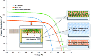
We report a back contact (BC) transparent conductive oxide (TCO)-less dye-sensitized solar cell (DSSC) fabricated utilizing a Co2+/3+ redox shuttle based electrolyte. A new strategy has been proposed for the reduction of the electrolyte layer by coating with a TiO2 nanoparticle spacer (TN spacer) with controlled thickness. The negatively charged TN spacer was found to decrease the diffusion of cobalt species through the TN spacer due to electrostatic interactions leading to a hampered photoconversion efficiency of 4.41%. This sluggish diffusion of bulky cobalt ions was amicably facilitated by passivating the negatively charged TN spacer surface with dye molecules. Facile transport of electrolyte ions in the nanopores of the passivated TN spacer was further confirmed by electrochemical impedance spectroscopy and estimation of the diffusion of Co3+ species in the nanopores of the passivated TN spacer using cyclic voltammetry. The TCO-less BC-DSSC in combination with the cobalt electrolyte fabricated in this novel device architecture exhibits a significantly improved photoconversion efficiency of 6.42% after the TN spacer was passivated with the porphyrin-based dye YD2-o-C8.


1. Introduction

The pioneering study by O'Regan and Grätzel in 1991 led to the possibility of attaining efficient solar-to-electrical energy conversion along with the cost-effectiveness of dye-sensitized solar cells (DSSCs).1 However, it has been realized that for the commercialization of DSSCs, a further decrease in the manufacturing cost as well as improvement in the photoconversion efficiency are inevitable. In the case of the conventional DSSC fabrication process, a mesoporous TiO2 film is coated onto a transparent conductive oxide (TCO) glass, such as a fluorine-doped tin-oxide (FTO) glass-substrate, which is one of the expensive components found in DSSCs.2 Kroon et al. reported that the two TCO glasses used in conventional DSSCs provide a cost burden of >20% of the total production cost of the DSSCs.3 Therefore, to make the DSSCs more cost effective, our group has attempted to fabricate a TCO-less BC-DSSC structure utilizing flexible metal mesh as a photoanode in combination with the I3/I redox mediator and ruthenium based sensitizer with the external power conversion efficiency of 5.56% under simulated solar irradiation.4 Li et al. demonstrated all stainless steel mesh-based DSSCs in combination with carbon ink counter electrode based on an iodine electrolyte with a reported photoconversion efficiency (PCE) of <1%.5 Kashiwa et al. reported all metal based TCO-less DSSCs by fabricating a thick and porous Ti electrode on a nanoporous TiO2 layer and the reported PCE (7.4%) was a slightly less than that of the TCO-based DSSC (8.4%).6 Fuke et al. have demonstrated a TCO-less DSSC, wherein thermally evaporated porous Ti metal deposited on a nanoporous TiO2 layer functioned as a back contacted current collector and named the structure as a back contact (BC) DSSC.7,8 To provide the cost-effectiveness to DSSCs, several efforts have also been made by various research groups utilizing a metal mesh as a flexible photoanode.9–12

For more than two decades, the I3/I redox couple has been extensively utilized for DSSCs owing to its fast dye regeneration and slow recombination.13 However, the I3/I redox couple has some limitations such as (i) partial visible light absorption by triiodide itself, which causes optical losses, (ii) it exhibits an aggressive nature towards the silver collecting grid and (iii) it requires a large over potential for dye-regeneration and ultimately raises the query for alternate redox mediators.14–16 In the recent past, several alternative redox mediators, such as cobalt based redox couples,16–22 TEMPO,23 ferrocene,24 disulphide/thiolate redox couple25 and nickel bis(dicarbollide),26 have been examined. Amongst them, redox mediators based on cobalt complexes have received a lot of attention because of their weak visible light absorption, lower corrosiveness towards the metal grid and more positive redox potential to produce a higher open-circuit voltage.16–22 Grätzel and co-workers reported a record PCE assisted by a very high open circuit voltage (Voc) of 0.96 V for a DSSC combining a novel porphyrin sensitizer along with a cobalt based redox mediator.27 However, a cobalt based redox mediator has some drawbacks; it shows faster recombination with the conduction band electrons in mesoporous TiO2 and sluggish dye regeneration.16,18,28 Various approaches have been investigated to minimize the recombination process by passivating the TiO2 surface using atomic layer deposition (ALD) of a thin insulating metal oxide.18,29–31

The mass transport problems of Co2+/3+ species were first introduced by Nusbaumer et al. in 200116 wherein they observed lower photocurrents at higher light intensities and about three times lower bulk diffusion coefficient as compared to that of I3.32 Nelson et al. reported that the diffusion of Co2+/3+ species through the mesoporous TiO2 is even more hampered, which is almost one order of magnitude slower than that of I3.32 This notable difference was due to the large and bulky size of the Co2+/3+ species and the electrostatic binding of the positively charged Co2+/3+ species with the negatively charged TiO2 surface.32 The mass transport problems of cobalt redox mediators in the pores of the photoanode have been significantly improved by optimizing the porosity and pore size of mesoporous TiO2 by Park and co-workers.33 Recently, Grätzel and co-workers used mesoporous TiO2 beads, which offer a high surface area, good scattering properties and high porosity to enhance the ionic diffusion of cobalt-based redox mediators.34

In an attempt to make DSSCs more cost-effective, we have already reported a TCO-less BC-DSSC based on cobalt redox mediator employing a porphyrin sensitizer with a PCE of 4.84%.35 In the TCO-less BC-DSSCs, dye monolayers are adsorbed on the high internal surface area of a mesoporous TiO2 film coated onto the flexible metal mesh. This metal mesh is placed over the porous polymer sheet (PTFE film; thickness: 35 μm), which absorbs the liquid electrolyte as well as avoids short-circuiting between the flexible photoanode and Pt counter electrode. The liquid electrolyte layer fills the pores of the electrode as well as the pores of the PTFE film. In our TCO-less BC-DSSCs device architecture, we realized that the porous polymer film (35 μm) was very thick leading to the hampered diffusion of Co2+/3+ species. To enhance the diffusion of Co2+/3+ species by reducing the thickness of the electrolyte absorbing layer, a novel strategy was attempted by utilizing a porous TN spacer stained with dye molecules instead of the porous PTFE film. TN bears a negative surface charge and offers attractive interactions with the positively charged cobalt species in the electrolyte, hampering ionic diffusion. To circumvent this problem, attempts have been made to passivate this negative surface charge by adsorbing dye monolayers on the TN spacers coated on the counter electrode.

2. Experimental

2.1 Materials and methods

All chemicals were purchased from commercially available sources and utilized as received. The Co(bpy)2+/3+ species were prepared as per our earlier publication.36 Ti-nanoxide (particle size 30 nm) PST-30NRT paste was purchased from JGC Catalysts and Chemicals Ltd., Japan. YD2-o-C8 dye was purchased from Everlight Chemical Co. Ltd., Taiwan. Organic dye Y123 was purchased from Dyenamo, Sweden. Indoline dye D131 was purchased from Mitsubishi Paper Mills Co. Ltd., Japan. The porous polymer sheet of polytetrafluoroethylene film (PTFE; H010A293D, thickness: 35 μm, pore size: 0.1 μm) was purchased from ADVANTEC, Japan. The molecular structures of the sensitizing dyes YD2-o-C8, Y123, D131, and Co complexes are shown in Fig. 1. Stainless steel (SS) mesh (SUS-730; wire diameter: 13 μm, space between the wires: 16 μm) was purchased from Asada mesh Co. Ltd., Japan. Electrochemical impedance spectroscopy (EIS) was performed with a frequency response analyser (Solartron Analytical, 1255B) connected to a Potentiostat (Solartron Analytical, 1287) under illumination and 2 mA constant current conditions employing a Yamashita Denso YSS-50A solar simulator in the frequency range of 5 mHz to 100 kHz at room temperature. The electrical impedance spectra were analysed using Z-View software (Solartron Analytical). Cyclic voltammetry was performed on an Automatic Polarization System (HSV-100, Hakuto Denko, Japan) employing a three-electrode setup consisting of a Pt working electrode, nanoporous TiO2 coated Pt as a counter electrode, and a Ag/AgCl reference electrode to investigate the diffusion of the cobalt species. The area of the nanoporous TiO2 film coated onto the Pt substrate was 1 cm2. The distance between the TiO2 coated Pt counter electrode and Pt working electrode was fixed at 2 cm. The electrolyte solution consisted of 2.2 mM Co(II) and 100 mM TBAPF6 in acetonitrile. The scan rates were varied from 10 mV s−1 to 80 mV s−1 during the CV measurements. The thickness of the nanoporous TiO2 film screen-printed onto the Pt counter electrode was measured using Dektak 6M (stylus profiler). The thickness of the nanoporous TiO2 layer screen-printed onto the Ti-protected metal mesh was calculated from the cross-sectional view employing scanning electron microscopy (SEM) on a NeoScope JCM-6000.
image file: c6ra04894c-f1.tif
Fig. 1 The molecular structures of D131, YD2-o-C8, Y123, and [Co(bpy)3]2+/3+.

2.2 TCO-less BC-DSSC fabrication

The TCO-less BC-DSSC was fabricated using SS mesh, which functions as a metallic support for the back contacted working electrode. We have already reported that protection of bare metal mesh is needed to improve the photovoltaic performance of the devices especially those based on cobalt based redox mediator.35 For this, a thin layer (300 nm) of Ti metal (SS mesh/Ti) was sputtered on both sides employing a sputtering apparatus (CFS-4EP-LL, Shibaura Mechatronics, Japan). The nanoporous TiO2 (30 nm) paste was coated onto the SS mesh/Ti using a screen-printing method followed by heating at 450 °C for 30 min. The TiO2 coated SS mesh/Ti was then dipped into the dye cocktail (YD2-o-C8[thin space (1/6-em)]:[thin space (1/6-em)]Y123 = 4[thin space (1/6-em)]:[thin space (1/6-em)]1) made from 0.2 mM YD2-o-C8 and 0.1 mM Y123 in ethanol at room temperature for 16 h. After dye adsorption, the TCO-less flexible photoanode was rinsed with the same solvent to remove the un-adsorbed dye. Pt (60 nm) was sputtered onto the FTO-glass substrate employing the same sputtering apparatus and used as a counter electrode. The same nanoporous TiO2 (30 nm) paste was screen-printed onto the Pt counter electrode and the substrate was soaked in the electrolyte solution to make the TN spacer. For the reference cell, a 35 μm thick PTFE film was placed over the Pt counter electrode to absorb the electrolyte solution. The cobalt based electrolyte solution consisted of Co(bpy)(II) complex (0.22 M), Co(bpy)(III) complex (0.033 M), tertiary butyl pyridine (TBP) (0.20 M) and LiClO4 (0.1 M) in acetonitrile. To assemble the device, a flexible SS mesh/Ti/TiO2/dye photoanode was placed over the nanoporous TiO2 coated Pt counter electrode. A transparent slide glass was placed over the flexible SS mesh/Ti/TiO2/dye photoanode to hold it. The cobalt based electrolyte was injected via a capillary tube. Finally, the device was sealed using epoxy resin. The whole device fabrication process is shown schematically in Fig. 2. A schematic of the TCO-less BC-DSSC fabricated in this present investigation is shown in the Fig. 3.
image file: c6ra04894c-f2.tif
Fig. 2 The device fabrication process used to prepare the TCO-less back contact dye-sensitized solar cells.

image file: c6ra04894c-f3.tif
Fig. 3 Schematic cross-sectional view of the TCO-less BC-DSSCs using porous PTFE film (a) and nanoporous TiO2 as the electrolyte absorbing layer (b).

2.3 Photovoltaic characterization

The photovoltaic characteristics of the TCO-less BC-DSSCs were measured using a solar simulator (CEP-2000 Bunko Keiki Co. Ltd, Japan) interfaced with a xenon lamp (Bunko Keiki BSO-X150LC) at 100 mW cm−2 under AM 1.5 conditions. The power of the light exposure from the solar simulator was fixed with an amorphous Si photodetector (Bunko Keiki BS-520 S/N 353) to avoid any discrepancy between the calibrated diode and the TCO-less BC-DSSCs. To measure the photovoltaic performance, the cell area was precisely controlled using a 0.2025 cm2 black metal mask.

3. Results and discussion

3.1 The photovoltaic performance of TCO-less BC-DSSCs using nanoporous TiO2 and PTFE as an electrolyte absorbing layer

The device configuration of the TCO-less BC-DSSCs used in this study is glass/dye/TiO2/Ti protected SS mesh/electrolyte/Pt FTO/glass, as shown in Fig. 3. The photocurrent density–voltage (JV) curves for the TCO-less BC-DSSCs sensitized with a dye cocktail of (YD2-o-C8[thin space (1/6-em)]:[thin space (1/6-em)]Y123 = 4[thin space (1/6-em)]:[thin space (1/6-em)]1) utilizing a Co(bpy)2+/3+ based electrolyte are shown in Fig. 4 and their corresponding photovoltaic and EIS parameters given in Table 1. The thickness of the nanoporous TiO2 film coated on the SS mesh/Ti to fabricate the photoanode was about 10 μm, which was maintained constant for all the devices. It is worth mentioning here that we have also used a TN spacer on a platinised FTO glass counter electrode as an electrolyte absorbing layer with two variations: (i) a bare TN spacer (7 μm) and (ii) a YD2-o-C8 stained TN spacer (7 μm) to absorb the electrolyte solution. We have also used a PTFE film spacer (35 μm) as a reference to absorb the electrolyte solution.
image file: c6ra04894c-f4.tif
Fig. 4 The photovoltaic characteristics of the TCO-less BC-DSSCs using a bare TiO2 film, YD2-o-C8 stained TiO2 film and PTFE film as an electrolyte absorber.
Table 1 The photovoltaic and EIS parameters for the TCO-less BC-DSSCs using porous TiO2 nanomaterials and PTFE film as an electrolyte absorbera
Parameters PTFE film (35 μm) YD2-o-C8 stained TiO2 (7 μm) Bare TiO2 (7 μm)
a Values in parenthesis indicate the average value of three independent cells along with their corresponding standard deviation.
Efficiency [%] 4.88 (4.71 ± 0.19) 5.81 (5.6 ± 0.19) 4.41 (4.12 ± 0.33)
FF 0.66 (0.65 ± 0.03) 0.64 (0.65 ± 0.021) 0.64 (0.63 ± 0.02)
Voc [V] 0.86 (0.86 ± 0.01) 0.88 (0.88 ± 0.006) 0.72 (0.71 ± 0.01)
Jsc [mA cm−2] 8.56 (8.43 ± 0.12) 10.31 (9.89 ± 0.54) 9.68 (9.26 ± 0.42)
Rs [Ω] 5.1 5.4 4.4
R1 [Ω] 4.9 3.2 4.3
R2 [Ω] 129.5 45.9 51.9
R3 [Ω] 75.8 36.4 62.9


From Fig. 4 and Table 1, it can be observed that the device using a bare TN spacer as the electrolyte absorbing layer exhibits a relatively lower photovoltaic performance with a short circuit current density (Jsc) of 9.68 mA cm−2, open circuit voltage (Voc) of 0.72 V and fill factor (FF) of 0.64 giving an external PCE of 4.41%. The reason for this lower photovoltaic performance can be attributed to the larger charge recombination as confirmed by the dark current–voltage (IV) characteristics shown in Fig. 4. The possible reason for this larger charge recombination is associated with the electrostatic interactions between the negatively charged bare TN surface and the positively charged oxidized cobalt Co3+ species, as shown in Fig. S1(a) of the ESI, 32 which slows down the diffusion of the Co3+ species in the pores and makes them available for rapid charge recombination. In addition, it has already been reported that the recombination rate between conduction band electrons and Co3+/2+ redox electrolytes is one order of magnitude higher than the recombination rate between the conduction band electrons and oxidized dye molecules.37

To clarify this differential behaviour, EIS measurements were also conducted. From the EIS measurements using the Nyquist plots, as shown in Fig. 5, we can explain the possible reasons for the lower photovoltaic performances. In general, the impedance spectrum shows three semicircles in the frequency range from 5 mHz to 100 kHz.38–40 The first semicircle is due to the impedance related to the charge transfer process at the Pt counter electrode in the high frequency region (Rs and R1). The second semicircle corresponds to the impedance related to the charge transport at the TiO2/dye/electrolyte interfaces in the mid frequency region (R2). Finally, the third semicircle is assigned to the impedance related to the ionic diffusion within the electrolyte in low frequency region (R3).


image file: c6ra04894c-f5.tif
Fig. 5 Nyquist plots for the TCO-less BC-DSSCs using a bare nanoporous TiO2 film, YD2-o-C8 protected nanoporous TiO2 film and PTFE film as an electrolyte absorber.

From Fig. 5, it is obvious that the impedance related to charge transfer at the Pt counter electrode in the high frequency region is almost the same in all cases (3–5 Ω). The impedance due to charge transport at the TiO2/dye/electrolyte interface (R2) is much higher for the device using a bare TN spacer (129.5 Ω) when compared to the devices using a YD2-o-C8 stained TiO2 nanoparticle spacer (45.9 Ω). Because the TiO2/dye/electrolyte interface for the photoanode is the same in all cases and photoanode is placed over the bare TN spacer filled with the electrolyte, this increase in impedance might be associated with the bare negatively charged TN surface present in the electrolyte layer, which causes the electrostatic interactions with the oxidized Co3+ species and slows down charge transport. The same possible electrostatic interactions are responsible for the relatively higher resistance observed in the low frequency region when a bare TN spacer is used as the electrolyte absorbing layer.

To prove this argument for facile ionic diffusion through the dye protected TN spacer, scan rate dependent cyclic-voltammetric (CV) measurement were also conducted and are shown in Fig. S2 of the ESI. The diffusion coefficients of the [Co(bpy)]3+ species for the bare TN spacer film and YD2-o-C8 protected TN film were estimated to be 4.24 × 10⁻⁶ cm2 s−1 and 5.11 × 10⁻⁶ cm2 s−1, respectively. Similar values obtained for the diffusion coefficient of cobalt species have also been reported by Nelson et al.32 This lower value for the diffusion coefficient (4.24 × 10⁻⁶ cm2 s−1) through the unprotected TN spacer corroborates that the diffusion of the Co3+ species is hampered in the nanopores of the nanoparticle spacer, which limits the photovoltaic performance of the device. As a result, dye regeneration is hampered and consequently, the Voc and Jsc values decrease. The Jsc decrease is explained by an increase in the resistance due to slow Co2+/3+ diffusion in the TN spacer and the Voc decrease is explained by slow dye regeneration. On the other hand, DSSCs using the YD2-o-C8 stained TN spacer, which decreases the possibility of charge recombination between electrons in the TiO2 photoanode and oxidized dyes exhibit significantly improved photovoltaic properties, as shown in the Fig. 4 and Table 1. The reason for this enhanced photovoltaic performance can be attributed to the suppressed charge recombination as confirmed by the dark current–voltage (JV) characteristics shown in the Fig. 4. The origin of this suppressed charge recombination can be understood from Fig. S1(b), wherein one can observe that when the surface of the bare TN spacer is stained with YD2-o-C8 dye, it avoids the possible electrostatic interactions between the negatively charged TN spacer and the positively charged oxidized cobalt Co3+ species and ultimately facilitates the diffusion of Co3+ species, which is responsible for higher PCE of 5.80% (Voc: 0.88 V, Jsc: 10.31 mA cm−2 and FF: 0.64).

The resistance observed in the low frequency region due to the ionic diffusion of Co3+ species (R3) within the nanoparticle spacer in the third semicircle is found to be the lowest. The reason for this lower resistance is that when the unprotected TN spacer is efficiently covered with the YD2-o-C8 dye, it avoids the unwanted electrostatic interactions between the negatively charged bare TN spacer and the Co3+ species, which results in the facile diffusion of the cobalt species. As a result, the dye regeneration gets faster and consequently, the Voc and Jsc values increase. The higher value obtained for the observed diffusion coefficient (5.11 × 10⁻⁶ cm2 s−1) in this case further corroborates that the diffusion of Co3+ species is improved in the TN spacer, which enhances the photovoltaic performance of the device. The device using porous PTFE film shows moderate photovoltaic characteristics giving a PCE of 4.88% (Voc: 0.86 V, Jsc: 8.56 mA cm−2 and FF: 0.66), as shown in the Fig. 4 and Table 1. The reason for getting this moderate photovoltaic performance was attributed to moderately suppressed charge recombination as confirmed by the dark IV characteristics shown in Fig. 4. Therefore, it can be attributed to a trade-off between the relatively facile diffusion of cobalt species due to neutral nature of porous PTFE film and the hampering of diffusion due to its large thickness. On the other hand, impedance due to the ionic diffusion of Co3+ species through the polymer PTFE film (35 μm) in the low frequency region (R3) is higher (75.8 Ω) than that of the other two devices based on the TN spacer (7 μm), which may be due to the relatively larger thickness (35 μm) of the PTFE film used as an electrolyte absorbing layer.35

3.2 The effect of the thickness of YD2-o-C8 stained TN spacer as an electrolyte absorbing layer

To optimize the thickness of the TN spacer to control the diffusion of Co3+ species, we varied the thickness of the TN spacer stained with the YD2-o-C8 dye keeping the same thickness of nanoporous TiO2 layer (about 10 μm) for the photoanodes. The thickness of the YD2-o-C8 stained TN spacer was varied from 5.5–16 μm and the corresponding photovoltaic characteristics for the TCO-less BC-DSSCs sensitized with the dye cocktail of (YD2-o-C8[thin space (1/6-em)]:[thin space (1/6-em)]Y123 = 4[thin space (1/6-em)]:[thin space (1/6-em)]1) employing Co(bpy)2+/3+ are shown in Fig. 6 and their corresponding photovoltaic and EIS parameters are listed in the Table 2.
image file: c6ra04894c-f6.tif
Fig. 6 The photovoltaic characteristics of the TCO-less BC-DSSCs with thickness variation of the porous TiO2 nanomaterials stained with the YD2-o-C8 dye coated onto the Pt counter electrode.
Table 2 The photovoltaic and EIS parameters for the TCO-less BC-DSSCs with thickness variation of the TN spacer protected with the YD2-o-C8 dye coated on the Pt-FTO as an electrolyte absorbera
Parameters YD2-o-C8 stained TN (5.5 μm) YD2-o-C8 stained TN (11 μm) YD2-o-C8 stained TN (16 μm)
a The values shown the parenthesis indicate the average value of three independent cells along with their corresponding standard deviation.
Efficiency [%] 6.42 (6.33 ± 0.10) 5.53 (5.36 ± 0.16) 4.67 (4.62 ± 0.06)
FF 0.66 (0.66 ± 0.006) 0.66 (0.66 ± 0.01) 0.65 (0.63 ± 0.015)
Voc [V] 0.89 (0.88 ± 0.012) 0.87 (0.87 ± 0.01) 0.85 (0.85 ± 0.006)
Jsc [mA cm−2] 10.88 (10.93 ± 0.05) 9.72 (9.38 ± 0.29) 8.45 (8.35 ± 0.14)
Rs [Ω] 3.4 2.9 3.5
R1 [Ω] 1.3 0.8 0.5
R2 [Ω] 48.4 49.3 65.8
R3 [Ω] 27.2 34.6 52.7


Fig. S3 in the ESI represents the correlation between the thickness of the dye stained TN spacer and the corresponding PCE of the TCO-less BC-DSSCs. From this figure, it is obvious that the efficiency decreases almost linearly with thickness. Therefore, the optimum TiO2 film thickness to the efficient TCO-less BC-DSSCs based on Co(bpy)2+/3+ redox electrolyte was found to be 5.5 μm. From Fig. 6, it can be observed that the Jsc and Voc values also followed the same trend in efficiency. In fact, attempts have also been made to use a TN spacer with a thickness less than 5 μm but the attempts failed due to short circuiting, most probably due to the manual pressing of the mesh based TCO-less photoanode and the counter electrode containing this thin TN spacer.

The decrease in efficiency with increasing thickness of the TN spacer was again clarified from the EIS measurements, as shown in Fig. 7. From Fig. 7, it is evident that the impedance related to charge transfer at the TiO2/dye/electrolyte interface (photoanode) in the mid frequency region (R2) is similar for the devices using a TN spacer with a thickness of 5.5 μm (48.4 Ω) and 11 μm (49.3 Ω), respectively, but larger for the device using a TN film with a thickness of 16 μm (65.8 Ω). We can conclude that the impedance due to charge transfer at the TiO2/dye/electrolyte interface (photoanode) remains the same up to a TiO2 film thickness of 11 μm and increases with further increase in the spacer thickness. Interestingly, we can see that the impedance due to the ion diffusion in the low frequency region (R3) increases with the thickness of the TN spacer. The larger impedance obtained with an increased thickness indicates that ion diffusion is hampered due to the sluggish diffusion of Co3+ ions and ultimately results in the hampered dye regeneration, which limits the photovoltaic performances of the devices and is in agreement with the IV characteristics obtained.41


image file: c6ra04894c-f7.tif
Fig. 7 EIS Nyquist plots for the TCO-less BC-DSSCs with thickness variation of the YD2-o-C8 stained nanoporous TiO2 film used as an electrolyte absorbing layer.

3.3 TCO-less BC-DSSCs using different dye stained TiO2 nanomaterials used as an electrolyte absorbing layer

TN spacers (5.5 μm) stained with YD2-o-C8 and D131 have been used to investigate TN spacer passivation capabilities and their resulting implication on the photovoltaic behavior. In this case, the thickness of the nanoporous TiO2 layer coated onto the Ti protected SS mesh working as photoanode was fixed with a thickness of about 10 μm. Fig. 8 shows the effect of the different dye stained TN spacers on the diffusion of oxidized cobalt Co3+ species and the corresponding photovoltaic parameters given in Table 3. From Fig. 8, it can be observed that the TCO-less BC-DSSC using a YD2-o-C8 stained TN spacer exhibits a much better PCE of 6.30% (Voc: 0.87 V, Jsc: 11.24 mA cm−2, FF: 0.65) when compared to the other device based on the D131 stained TN spacer with an external PCE of 3.37% (Voc: 0.70 V, Jsc: 7.95 mA cm−2, FF: 0.61). From the dark IV characteristics (Fig. 8) as well as EIS measurements (Fig. S4), it is clear that the device using the YD2-o-C8 stained TN spacer shows a greatly suppressed dark current as well as the lowest impedance related to ion diffusion in the low frequency region, which is responsible for achieving this much improved photovoltaic behaviour.
image file: c6ra04894c-f8.tif
Fig. 8 The photovoltaic characteristics of the TCO-less BC-DSSCs with different dye stained nanoporous TiO2 layer coated onto the Pt counter electrode used as an electrolyte absorber.
Table 3 The effect of different dye stained nanoporous TiO2 layer coated onto the Pt counter electrode used as an electrolyte absorber on the photovoltaic performance of the TCO-less BC-DSSCsa
Parameters D131 stained TiO2 YD2-o-C8 stained TiO2
a The values shown the parenthesis indicate the average value of three independent cells along with their corresponding standard deviation.
Efficiency [%] 3.37 (3.31 ± 0.09) 6.30 (6.21 ± 0.08)
FF 0.61 (0.61 ± 0.015) 0.65 (0.65 ± 0.006)
Voc [V] 0.70 (0.70 ± 0.006) 0.87 (0.88 ± 0.012)
Jsc [mA cm−2] 7.95 (7.87 ± 0.49) 11.24 (10.88 ± 0.34)


The origin of this suppressed dark current as well as the facile diffusion of Co3+ species through the YD2-o-C8 covered TN spacer was further confirmed by CV measurements. The diffusion coefficients of the [Co(bpy)]3+ species diffusing through the TN spacer stained with YD2-o-C8 and D131 were estimated to be 5.11 × 10⁻⁶ cm2 s−1 and 3.24 × 10⁻⁶ cm2 s−1, respectively, using the Randles–Sevcik equation (Fig. S5, ESI). A comparatively higher value of the diffusion coefficient (5.11 × 10⁻⁶ cm2 s−1) of [Co(bpy)]3+ for the YD2-o-C8 protected TN spacer indicates that the diffusion of cobalt species is relatively faster through the TN spacer, which results in the faster dye regeneration, as well as higher Voc, Jsc and FF. Herein, we would like to emphasize that the structure of the dye also plays an important role in protecting the surface of the bare TN spacer. When the bare TN spacer is protected with YD2-o-C8 dye, its long alkyl chain can impair the electrostatic interactions between the negatively charged TN spacer and Co3+ species more efficiently, which expedites the diffusion of the Co3+ species through the porous TN spacer. The relatively lower PCE of 3.37% obtained using the D131 covered TN spacer is associated with a larger charge recombination as corroborated by the dark IV characteristics (Fig. 8) and the relatively higher impedance associated with the ion diffusion in the low frequency region observed in the EIS measurements (Fig. S4). This lower value for the diffusion coefficient (3.24 × 10⁻⁶ cm2 s−1) of [Co(bpy)]3+ for the D131 stained TN spacer indicates that the diffusion of the cobalt species is relatively slower through the TN spacer, which results in sluggish dye regeneration and poor photovoltaic performance. The D131 has no long alkyl chain and may not be effective in passivating the nanoporous TiO2 spacer sufficiently.

4. Conclusions

TCO-less back contact DSSCs utilizing cobalt based redox shuttle have been successfully fabricated by varying the thicknesses of the TN spacer and a thickness of 5.5 μm was found to be optimal. This strategy has been adopted as a replacement of thick polymer PTFE film (35 μm) to enhance the diffusion of bulky Co2+/3+ species by decreasing the thickness of the electrolyte absorbing layer. When the surface of the bare TN spacer coated on the counter electrode was protected with YD2-o-C8 dye, it effectively impedes the electrostatic attractive forces between the negatively charged TiO2 surface and the positively charged Co3+ species owing to its long alkyl chain compared to D131 and ultimately results in the facile diffusion of the Co3+ species through the porous TN spacer yielding the best PCE of 6.42%.

Acknowledgements

This study is supported by the Strategic Promotion of Innovative Research and Development (S-Innovation) Program of Japan Science and Technology under the Japanese Government.

Notes and references

  1. B. O'Regan and M. Grätzel, Nature, 1991, 353, 737–740 CrossRef.
  2. H. Greijer, L. Karlson, S. T. Lindquist and A. Hagfeldt, Renewable Energy, 2001, 23, 27–39 CrossRef CAS.
  3. J. M. Kroon, N. J. Bakar, H. J. P. Smit, P. Liska, K. R. Thampi, P. Wang, S. M. Zakeeruddin, M. Gratzel, A. Hinsch, S. Hore, U. Wurfel, R. Sastrawan, K. Skupien and G. E. Tulloch, Prog. Photovolt: Res. Appl., 2007, 15, 1–18 CrossRef CAS.
  4. Y. Yoshida, S. S. Pandey, K. Uzaki, S. Hayase, M. Kono and Y. Yamaguchi, Appl. Phys. Lett., 2009, 94, 093301 CrossRef.
  5. H. Li, Q. Zhao, H. Dong, Q. Ma, W. Wang, D. Xu and D. Yu, Nanoscale, 2014, 6, 13203–13212 RSC.
  6. Y. Kashiwa, Y. Yoshida and S. Hayase, Appl. Phys. Lett., 2008, 92, 033308 CrossRef.
  7. N. Fuke, A. Fukui, Y. Chiba, R. Komiya, R. Yamanaka and L. Han, J. Appl. Phys., 2007, 46, L420–L422 CrossRef CAS.
  8. N. Fuke, A. Fukui, Y. Komiya, A. Islam, Y. Chiba, M. Yanagida, R. Yamanaka and L. Han, Chem. Mater., 2008, 20, 4974–4979 CrossRef CAS.
  9. X. Fan, F. Wang, Z. Chu, L. Chen, C. Zhang and D. Zou, Appl. Phys. Lett., 2007, 90, 073501 CrossRef.
  10. C. S. Rustomji, C. J. Frandsen, S. Jin and M. J. Tauber, J. Phys. Chem. B, 2010, 114, 14537–14543 CrossRef CAS PubMed.
  11. W. He, J. Qiu, F. Zhuge, X. Li, J. Lee, Y. Kim, H. Kim and Y. Hwang, Nanotechnology, 2012, 23, 225602 CrossRef PubMed.
  12. Y. Wang, H. Yang, Y. Liu, H. Wang, H. Shen, J. Yan and H. Xu, Prog. Photovolt: Res. Appl., 2010, 18, 285–290 CAS.
  13. G. Boschloo and A. Hagfeldt, Acc. Chem. Res., 2012, 42, 1819–1826 CrossRef PubMed.
  14. P. Bonhote, M. Gratzel, M. Jirousek, P. Liska, N. Pappas, N. Vlachopoulos, C. V. Planta and L. Walder, 10th International Conference on Photochemical Conversion and Storage of Solar Energy (IPS-10), 1994, Abstract C2 Search PubMed.
  15. G. Oskam, B. V. Bergeron, G. J. Meyer and P. C. Searson, J. Phys. Chem. B, 2001, 105, 6867–6873 CrossRef CAS.
  16. H. Nusbaumer, J.-E. Moser, S. M. Zakeeruddin, M. K. Nazeeruddin and M. Gratzel, J. Phys. Chem. B, 2001, 105, 10461–10464 CrossRef CAS.
  17. S. A. Sapp, C. M. Elliott, C. Contado, S. Caramori and C. A. Bignozzi, J. Am. Chem. Soc., 2002, 124, 11215–11222 CrossRef CAS PubMed.
  18. B. M. Klahr and T. W. Hamann, J. Phys. Chem. C, 2009, 113, 14040–14045 CAS.
  19. S. M. Feldt, E. A. Gibson, E. Gabrielsson, L. Sun, G. Boschloo and A. Hagfeldt, J. Am. Chem. Soc., 2010, 132, 16714–16724 CrossRef CAS PubMed.
  20. A. Yella, H.-W. Lee, H. N. Tsao, C. Yi, A. K. Chandiran, M. K. Nazeeruddin, E. W.-G. Diau, C. Y. Yeh, S. M. Zakeeruddin and M. Gratzel, Science, 2011, 334, 629–634 CrossRef CAS PubMed.
  21. S. M. Feldt, G. Wang, G. Boschloo and A. Hagfeldt, J. Phys. Chem. C, 2011, 115, 21500–21507 CAS.
  22. J.-H. Yum, E. Baranoff, F. Kessler, T. Moehl, S. Ahmad, T. Bessho, A. Marchioro, E. Ghadiri, J.-E. Moser and M. Gratzel, Nat. Commun., 2012, 3, 631 CrossRef PubMed.
  23. Z. Zhang, P. Chen, T. N. Murakami, S. M. Zakeeruddin and M. Gratzel, Adv. Funct. Mater., 2008, 18, 341–346 CrossRef CAS.
  24. T. Daeneke, T.-H. Kwon, A. B. Holmes, N. W. Duffy, U. Bach and L. Spiccia, Nat. Chem., 2011, 3, 211–215 CrossRef CAS PubMed.
  25. M. Wang, N. Chamberland, L. Breau, J.-E. Moser, R. Humphry-Baker, B. Marsan, S. M. Zakeeruddin and M. Grätzel, Nat. Chem., 2010, 2, 385–389 CrossRef CAS PubMed.
  26. T. C. Li, A. M. Spokoyny, C. She, O. K. Farha, C. A. Mirkin, T. J. Marks and J. T. Hupp, J. Am. Chem. Soc., 2010, 132, 4580–4582 CrossRef CAS PubMed.
  27. S. Mathew, A. Yella, P. Gao, R. Humphry-Baker, B. F. E. Curchod, N. Ashari-Astani, I. Tavernelli, U. Rothlisberger, M. K. Nazeeruddin and M. Grätzel, Nat. Chem., 2014, 6, 242–247 CrossRef CAS PubMed.
  28. S. Nakade, Y. Makimoto, W. Kubo, T. Kitamura, Y. Wada and S. Yanagida, J. Phys. Chem. B, 2005, 109, 3488–3493 CrossRef CAS PubMed.
  29. J. W. Ondersma and T. W. Hamann, J. Phys. Chem. C, 2010, 114, 638–645 CAS.
  30. A. K. Chandiran, M. K. Nazeeruddin and M. Gratzel, Adv. Funct. Mater., 2013, 24, 1615–1623 CrossRef.
  31. T. W. Hamann, O. K. Farha and J. T. Hupp, J. Phys. Chem. C, 2008, 112, 19756–19764 CAS.
  32. J. J. Nelson, T. J. Amick and C. M. Elliott, J. Phys. Chem. C, 2008, 112, 18255–18263 CAS.
  33. H.-S. Kim, S.-B. Ko, I.-H. Jang and N.-G. Park, Chem. Commun., 2011, 47, 12637–12639 RSC.
  34. L.-P. Heiniger, F. Giordano, T. Moehl and M. Grätzel, Adv. Energy Mater., 2014, 4, 1400168 Search PubMed.
  35. M. Z. Molla, N. Mizukoshi, H. Furukawa, Y. Ogomi, S. S. Pandey, T. Ma and S. Hayase, Prog. Photovolt: Res. Appl., 2015, 23, 1100–1109 CrossRef CAS.
  36. M. J. Marchena, G. de Miguel, B. Kohen, J. A. Organero, S. Pandey, S. Hayase and A. Douhal, J. Phys. Chem. C, 2013, 117, 11906–11919 CAS.
  37. P. Piatkowski, C. Martin, M. R. di-Nunzio, B. Cohen, S. Pandey, S. Hayase and A. Douhal, J. Phys. Chem. C, 2014, 118, 29674–29687 CAS.
  38. R. Kern, R. Sastrawan, J. Ferber, R. Stangl and J. Luther, Electrochim. Acta, 2002, 47, 4213–4225 CrossRef CAS.
  39. J. Lagemaat, N.-G. Park and A. J. Frank, J. Phys. Chem. B, 2000, 104, 2044–2052 CrossRef.
  40. M. C. Bernard, H. Cachet, P. Falaras, A. H. L. Goff, M. Kalbac, I. Lukes, N. T. Oanh, T. Stergiopoulos and I. Arabatzis, J. Electrochem. Soc., 2003, 150, E155–E164 CrossRef CAS.
  41. M. Topic, A. Campa, M. Filipic, M. Berginc, U. O. Krasovec and F. Smole, Curr. Appl. Phys., 2010, 10, S425–S430 CrossRef.

Footnote

Electronic supplementary information (ESI) available. See DOI: 10.1039/c6ra04894c

This journal is © The Royal Society of Chemistry 2016
Click here to see how this site uses Cookies. View our privacy policy here.