
Vertically grown nanowire crystals of dibenzotetrathienocoronene (DBTTC) on large-area graphene†
B.
Kim‡
a,
C.-Y.
Chiu‡
b,
S. J.
Kang
c,
K. S.
Kim
d,
G.-H.
Lee
e,
Z.
Chen
f,
S.
Ahn
g,
K. G.
Yager
 h,
J.
Ciston
i,
C.
Nuckolls
j and
T.
Schiros
*kl
h,
J.
Ciston
i,
C.
Nuckolls
j and
T.
Schiros
*kl
aDepartment of Chemistry, New Jersey City University, Jersey City, NJ 07305, USA
bPPG Industries Inc., Monroeville Chemicals Center, Monroeville, PA 15146, USA
cSchool of Energy and Chemical Engineering, Ulsan National Institute of Science and Technology, Ulsan 608-798, South Korea
dDepartment of Physics and Graphene Research Institute, Sejong University, Seoul 05006, South Korea
eDepartment of Material Science and Engineering, Yonsei University, Seoul 03722, South Korea
fDepartment of Chemistry, Emory University, Atlanta, GA 30322, USA
gInstitute of Advanced Composite Materials, Korea Institute of Science and Technology, Wanju 565-905, Korea
hCenter for Functional Materials, Brookhaven National Laboratory, Upton, NY 11973, USA
iMaterials Sciences Division, Lawrence Berkeley National Laboratory, Berkeley, CA 94720, USA
jDepartment of Chemistry, Columbia University, New York, NY 10027, USA
kMaterials Research Science and Engineering (MRSEC), Columbia University, New York, NY 10027, USA. E-mail: ts2526@columbia.edu
lFashion Institute of Technology, State University of New York, New York, NY 10001, USA
First published on 1st June 2016
Abstract
We demonstrate controlled growth of vertical organic crystal nanowires on single layer graphene. Using Scanning Electron Microscopy (SEM), high-resolution transmission electron microscopy (TEM), and Grazing Incidence X-ray Diffraction (GIXD), we probe the microstructure and morphology of dibenzotetrathienocoronene (DBTTC) nanowires epitaxially grown on graphene. The investigation is performed at both the ensemble and single nanowire level, and as a function of growth parameters, providing insight of and control over the formation mechanism. The size, density and height of the nanowires can be tuned via growth conditions, opening new avenues for tailoring three-dimensional (3-D) nanostructured architectures for organic electronics with improved functional performance.
Introduction
Growth of organic crystals on two-dimensional (2-D) and layered nanomaterials1–4 has recently garnered great interest not only in terms of fundamental properties of these heterojunctions but also due to their potential to impact organic electronics, optimizing charge transport and extraction in devices optimized for a particular application via tailored nano- and micro-structures. Graphene, a single 2-D sheet of carbon atoms, has been rigorously investigated for its promise to impact post-silicon electronics, especially as a universal contact. This promise is born from its exceptional optoelectronic and mechanical properties owed to its 2-dimensional nature, including high transparency,5 flexibility,5–8 conductivity,9,10 an atomically well-defined interface free of charge traps and dissipative barriers,11,12 and a versatile work function tunable by chemical13–16 and contact doping.17The ability to tune the interaction between organic molecules and graphene to create controlled 3-D structures represents a challenge with enormous potential to advance organic electronics. Since low mobility and poor charge transport represent the major bottlenecks for advancement of organic electronics, there is a demand for further study on direct growth of organic crystals on substrates as a conduit towards overcoming these obstacles. Epitaxial crystal growth, driven by spontaneous self-assembly, is an efficient way to lower resistance at the substrate–film interface by ensuring intimate interfacial contact and molecular alignment. We recently demonstrated epitaxial growth of rubrene crystals on h-BN substrates with mobilities comparable to their single crystal counterparts; graphene contacts to these films showed ohmic injection and high on–off ratios relative to gold counterparts.11
A deeper understanding of low-dimensional and interfacial assembly at the surface of 2-D materials is essential to tuning the emergent electronic properties of future heterojunction architectures. A key question is whether we can exploit the crystallographically and atomically well-defined surface of graphene to facilitate epitaxial growth of organic semiconductor single crystals over large areas, with control over the morphology of crystals and molecular packing orientation favourable to transport and extraction of charge carriers for a given application. A crucial challenge in this regard is to find materials that demonstrate a strong interaction with graphene. In this context, graphene-like organic molecules, such as coronene, represent good candidates for directed crystal growth due to their structural similarity and the overlap of sp2-hybridized orbitals of graphene and organic semiconductors.18 Strong π–π interaction between graphene and various polycyclic aromatic compounds has been already proven by several studies.19–22 In this study, we report on the vertical growth of organic nanowire crystals of dibenzotetrathienocoronene (DBTTC) on large-scale graphene films. Within the benzocoronene family, DBTTC is particularly remarkable in that it has one-dimensional columnar packing crystal structure, as shown in Fig. 1, presumably due to its sulfur-to-sulfur interlocking interaction as well as its contorted molecular conformation.23 Moreover, we have previously demonstrated that a network of hexyl chain substituted DBTTC cables formed by a temperature-induced self-assembly process templates formation of a reticulated organic heterojunction with C60 with improved photovoltaic efficiency.24 Here, motivated by exploration of graphene as a transparent electrode and the structural match of the coronene core of DBTTC to the graphene lattice, we demonstrate another manifestation of self-assembly by growing DBTTC crystals on graphene with a well-defined vertical nanopillar structure. By studying the microstructure and morphology of the DBTTC crystals as a function of growth conditions and substrate, we gain insight on the growth mechanism of the nanowires, which are uniquely vertical on graphene substrates, while demonstrating control over their size, density and height. The molecular-scale packing and crystallographic orientation is probed at the ensemble level with Grazing Incidence X-ray Diffraction (GIXD) and at the single fiber level with transmission electron microscopy (TEM), and correlated to morphology with scanning electron microscopy (SEM). The findings provide fundamental insight central to realization of graphene's full potential to impact post-silicon electronics applications, as well as the ability to generate ordered 3-D organic heterojunctions with controlled microstructure and morphology.
 | ||
| Fig. 1 (a) Chemical structure of dibenzotetrathieno-coronene (DBTTC), (b) front view of molecular columns, and (c) side view of the columnar molecular packing of DBTTC with unit cell and axes overlaid. | ||
Experimental methods
Sample preparation
Pristine, single-layer graphene was prepared by thermal chemical vapor deposition (CVD) method performed by Xuesong Li et al.7 As a pretreatment, copper foil (50 µm thick), used as a catalyst substrate, was placed in a tube furnace and purged with ultrahigh-purity argon gas (99.9999%) under 10–3 torr vacuum to have constant pressure (1.2 Torr). Then the system was annealed at 1000 °C with flow of ultra-high-purity hydrogen gas (6.4 × 10⁻² Torr) for 10 minutes. After the annealing step, the growth was triggered by adding methane gas (170 SCCM (mL min−1), 1.7 Torr) for 18 minutes. The system was then purged with argon gas and slowly cooled down to room temperature.The graphene film produced was then transferred to a Si substrate with a 300 nm native oxide layer selected to optimize graphene visualization with optical microscopy.25 To accomplish the transfer, graphene grown copper foil was cut into the desired size (1.5 × 1.5 cm2) and mounted onto glass substrate with tape. Then 950 poly(methyl methacrylate) PMMA (A5) was spincast on the graphene grown copper film (5000 rpm for 60 seconds). The spincast film was baked at 50 °C for 10 minutes to ensure complete drying. The foil was then floated on FeCl3 solution (30% wt) to etch copper foil, leaving graphene supported by the PMMA film. After the copper foil was fully etched, the transparent graphene film supported by PMMA was placed onto SiO2 an substrate and dried at 50 °C. PMMA was then removed by acetone, leaving a pristine single layer of graphene on the SiO2 substrate. The samples were annealed at 300 °C under 150 SCCM of argon and 10 SCCM of hydrogen for an hour to remove any residuals from the transfer process. The Raman spectrum of the transferred graphene sheet (Fig. S1†) showed ∼0.3 G![[thin space (1/6-em)]](https://www.rsc.org/images/entities/char_2009.gif) :2D intensity ratio and a narrow 2D peak bandwidth (32 cm−1), indicating single-layer graphene.26 An almost undetectable D peak verified the high quality of the graphene film, except for a slight upshift of the G peak and 2D peak to 1587 and 2694 cm−1, respectively, possibly due to residual iron chloride from the transfer procedure.
:2D intensity ratio and a narrow 2D peak bandwidth (32 cm−1), indicating single-layer graphene.26 An almost undetectable D peak verified the high quality of the graphene film, except for a slight upshift of the G peak and 2D peak to 1587 and 2694 cm−1, respectively, possibly due to residual iron chloride from the transfer procedure.
DBTTC nanocrystals were grown on single layer graphene by physical vapor deposition in a temperature gradient furnace.27 DBTTC powder (2 mg) was placed at the high temperature zone (330–350 °C), while the graphene-coated substrate was placed in the low temperature zone (139–152 °C). After the sample was loaded, the system was purged with argon gas and vacuum was applied to control pressure. Temperature of the system was then gradually increased to the target temperature (50 °C min−1). After 6 hours of growth, the system was slowly cooled down and the sample was retrieved for further analysis. In this study, temperature and pressure were varied to probe their effects on crystal size and density; pressure was varied from 0.58 ± 0.01 Torr (100 SCCM of argon) to 1.20 ± 0.01 Torr (300 SCCM of argon), and DBTTC source temperature was varied from 330 to 350 °C. Further change of temperature and pressure resulted in excessive or negligible deposition of DBTTC, so crystal morphology was monitored in the range of conditions described above. To understand the growth mechanism, we also investigated the time dependence of crystal growth, varying growth time from 2 hours to 6 hours. All the crystals were imaged by Hitachi 4700 Secondary Electron Microscope (SEM) with 45°-tilted angle.
Measurements
Grazing Incidence X-ray Diffraction (GIXD) was performed at the National Synchrotron Light Source (NSLS) of Brookhaven National Laboratory on beamline X-9 at and at Stanford Synchrotron Radiation (SSRL) Lightsource on beamline 11-3 at a photon energies of 14.0 keV and 12.7 keV, respectively. The incident X-ray beam had a grazing incidence angle with the sample surface, which was increased from 0.07° to 0.30° in ∼0.03° steps for multiple (at least 3) spots across the sample surface. A Photonic Science WAXS (Wide Angle X-ray Scattering) detector (pixel size of 0.11 mm) at the NSLS or a 2D MAR345 (pixel size of 0.15 mm) at SSRL was used to detect the X-ray beam scattered from the sample and to convert the scattering vector, obtained as the difference in momentum between incoming and outgoing momentum vectors, into a reciprocal space (q-space) image of the scattered beam. The sample to detector distances for the data shown here, calibrated with a LaB6 polycrystalline standard, were 270.0 mm and 399.9 mm at NSLS and SSRL, respectively. The samples were kept under vacuum at NSLS and under a helium atmosphere at SSRL during measurement to minimize damage to the films from the intense X-ray beam and eliminate X-ray scattering from air. Additional details are provided in the ESI.†TEM imaging and SAED patterns were measured at Center of Functional Materials (CFN) of Brookhaven National Laboratory using JEOL JEM2100F.
Results and discussion
DBTTC nanowire growth
The morphological variation of DBTTC crystals formed at different temperatures and pressures is shown in Fig. 2. DBTTC formed vertical nanowire crystals on graphene sheets transferred to SiO2 under all growth conditions investigated. This supports the intuition that the π–π stacking system and molecular conformation of DBTTC are well matched to that of graphene, and that this similarity opens an opportunity for directed crystal growth. Under the observed conditions, crystals grew longer increased temperature. For example, for T = 330 °C, and P = 0.58 Torr, crystals were 5 µm long in average, while crystals for T = 350 °C and P = 0.58 Torr were longer than 10 µm. When pressure was increased, both an increase in thickness and decrease in length of the nanowires were observed. These results also correspond well with crystal film morphology study of CuPc on graphene substrate performed by Xiao et al.28 | ||
| Fig. 2 Temperature and pressure dependence of DBTTC crystal growth on graphene film and average size of crystals (the scale bar on the right bottom stands for 1 µm). | ||
The time dependence of the crystal growth provides insight to the underlying mechanism. Gradual changes in the morphology of the crystal film were observed as the duration of growth was increased stepwise from 2 to 6 hours (Fig. 3). In the 2 hour reaction, the crystals were indistinguishable and uniformly covered the graphene surface. After 2 hours, crystal growth begins with arbitrary crystallite deposition (Fig. 3).
 | ||
| Fig. 3 Time dependence of DBTTC crystal growth (340 °C, 200 SCCM, 4 mg of DBTTC) 2 hour, 2.5 hour, 3 hour, 4 hour and 6 hour growth (from left to right). | ||
After 2.5 hours growth time, rod-like crystals appeared but the growth direction was arbitrary. Between 3 and 5 hours growth time, interesting changes are observed: the number of horizontal crystals decreased, with only vertical crystals surviving after 5 hours. This result confirms orientation selectivity of DBTTC crystals on single layer graphene on SiO2. We conclude that Ostwald ripening dominates the growth of DBTTC; DBTTC molecules wet on graphene film in the early growth stage and then slowly nucleate to form vertical crystals.
GIXD measurements of DBTTC nanowire films on graphene
We investigate the structure and molecular scale packing of DBTTC crystals on graphene at the ensemble level with GIXD. Fig. 4 shows the 2-D reciprocal (q-) space diffraction patterns for a series of films grown with different conditions measured at an incident angle of 0.07°, below the critical angle of the films, measured at NSLS beamline X9 (experimental details provided in Methods and ESI†). We note that the salient features in the GIXD discussed are observed at higher incident angles (even up to local specular measurements), confirming that the presented results are representative of the bulk of the film and not dominated by surface effects. Transmission-mode X-ray diffraction of single crystals of DBTTC indicates a triclinic unit cell with columnar packing of the DBTTC molecules (see Fig. S2 and S3 in the ESI†); the q-values of the peaks observed in GIXD are in good agreement with the single crystal pattern reflections. This suggests that the DBTTC packing is not perturbed by the surface-grown method here described. Crystallographic order repeated in- and out-of-plane of the DBTTC film are indicated by intensity along the qr and qz axes, respectively.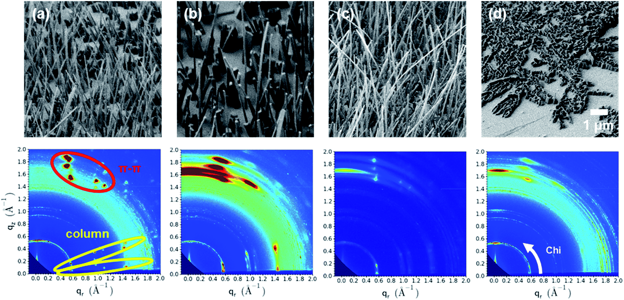 | ||
| Fig. 4 SEM images and corresponding GIXD spectrums of DBTTC crystals grown on graphene transferred to SiO2. (a) 340 °C, 200 SCCM, 6 hour growth, (b) 350 °C, 300 SCCM, 6 hour growth, (c) 340 °C, 100 SCCM, 6 hour growth, and (d) 340 °C, 200 SCCM, 2 hour growth. The amount of DBTTC in the feedstock was fixed to 2 mg. | ||
Certain diffraction features characterize all DBTTC films on graphene independent of the particular growth conditions explored, from which we can infer the molecular packing and substrate-crystallographic orientation of the films using the unit cell obtained from single crystal diffraction as a reference. These include the trio of reflections between 1.65 and 2.0 Å−1 and neighboring doublet of reflections at q ∼ 1.8 Å−1, which are all related to the π-stacking of the DBTTC molecules and correspond to repeat distances of ∼3.65 Å. Intensity at q = 0.51, 0.5399 and 0.542 Å−1 corresponds to the (001), (01−1) and (010) reflections of the DBTTC unit cell, respectively, which describe the packing of the molecular DBTTC columns; higher order reflections of the low-q (∼0.5 Å−1) peaks are observed at 0.9, 1.0 and 1.40 Å−1 are also observed (see Fig. 4a). The sharpness of the molecular packing peaks and the presence of higher order reflections along qr indicate a highly ordered in-plane packing of the molecular columns, i.e. the crystals consist of rigidly packed 1-D columns which share the vertical axis of the crystal growth.
In contrast to the molecular column peaks which are always sharp, if not intense, it is clear from Fig. 4 that the angular spread of the π-stacking reflections is strongly dependent upon DBTTC growth conditions, varying from ∼0.05 to 0.3 Å−1 along the Chi-arc direction (indicated in Fig. 4b (bottom)), with much less variance along the q direction (∼0.05–0.1 Å−1). This is not unexpected in columnar crystal growth, as deviations from vertical orientation observed in the SEM images of Fig. 2 would produce a Chi variation in the GIXD. However, the GIXD reflections attributed to columnar packing are quite narrow (<0.05 Å−1), with much less spread along Chi, independent of the growth conditions. Moreover, we observe both (11−1) and (10−1) reflections (Fig. S2 and S3†), corresponding to repeat distances associated with the DBTTC plate-like core and the “arms” which protrude from the core at a ∼20° angle, respectively with comparable intensity. This suggests a flexibility of the individual molecules to interact with the graphene through either the π-orbitals of the structurally matched DBTTC core as well as to “anchor” on the substrate through interaction with the hydrogen atoms of the arms of the molecule, which are sensitive to variation of charge density along the graphene surface. This flexibility would facilitate the vertical stacking and manifest as a larger angular spread of the diffraction peaks relative to those of the column packing for the same crystals.
In addition to the well-defined, localized peaks discussed previously, sets of weakly textured rings are also present in the GIXD patterns (Fig. 4). This combination suggests a bimodal distribution in the films; i.e. two classes of crystallites. We attribute the well-defined peaks to the primary, highly oriented, crystalline rods achieved with extended growth time as indicated in Fig. 4. The weakly textured rings and broad prominent feature centered at qz = 1.72 Å−1 (not identified with a DBTTC crystal plane spacing) are attributed to the residual isotropic crystals that characterize the films in the initial stages of growth seen in Fig. 2d. Thus, the ratio of the integrated intensity of the bright, localized diffraction spots and that of the rings provides an estimate of the volume fraction of nanowire crystals and residual isotropic crystallites. Consistent with the SEM images (Fig. 4 (top)), we estimate that the films grown for 6 hours with at least 0.9 torr (200 SCCM) (Fig. 4a and b) exhibit the highest fraction of well-ordered nanowires epitaxially grown on graphene, which we expect to facilitate charge transport and separation in device.
To gain additional insight into the nature of the growth mechanism of the vertical DBTTC nanowires on transferred graphene, in Fig. 5 we use SEM (top) and GIXD (bottom) to investigate DBTTC crystal growth on alternate surfaces under the same growth conditions (340 °C, 100 SCCM, 6 hour growth and 2 mg of DBTTC powder). Here we prepared three different substrates for crystal growth: highly-oriented pyrolytic graphite (HOPG), CVD-grown graphene on copper foil, SiO2 and mica substrate. Both HOPG and graphene on copper foil contain the same planar π-orbitals on surface as our graphene/SiO2 samples have, and we investigated the effect of π–π interaction between substrate and DBTTC. SiO2 and mica substrates are used to see if surface roughness has any effect on crystal growth.
 | ||
| Fig. 5 SEM images (top) and GIXD 2-D reciprocal space images (bottom) measured at a 0.07° incident angle for DBTTC crystals grown on: (a) HOPG; (b) CVD-grown graphene on copper foil; and (c) SiO2. | ||
In striking contrast to the vertical nanowires on graphene/SiO2, the orientation of DBTTC crystals grown on SiO2 (Fig. 5c) and mica (Fig. S6†), is horizontal and arbitrary, presumably due to the lack in π-orbital matching interaction. Yet, despite its π-orbital surface, even HOPG substrate did not grow vertical nanowire DBTTC crystals (Fig. 5a).
Moreover, although vertically grown, DBTTC crystals on CVD graphene on copper foil were also quite different from the nanowires on the transferred graphene, forming wall-like 2-D crystals rather than 1-D nanowires (Fig. 5b). We note that the varying surface roughness of the substrates may also contribute to the variation in crystal morphology with substrate, although to a lesser degree. For instance, AFM and STM studies show that transferred graphene film on SiO2 has about 1.5 nm RMS surface roughness while HOPG surface is almost flat with less than 1 nm roughness (Fig. S7 and S8†). Graphene-grown copper foil also showed significant surface roughness with preferential puckered pattern that was formed by thermal annealing of CVD growth process. Crystal morphology of graphene on copper foil shows that DBTTC crystals are grown along the puckers of copper foil, which results in wall-like 2-D crystals. In contrast, the surface roughness on HOPG is negligible and π-orbital interaction between graphite and DBTTC predominates; consequently, DBTTC molecules spread out on the surface rather than stack one on another.
The 2-D diffraction patterns shown in Fig. 5 (bottom) reveal microstructural differences between DBTTC grown on transferred graphene Fig. 4 (bottom) and on alternate surfaces. For instance, Fig. 5c (bottoms) shows diffraction intensity at q-values characteristic of triclinic DBTTC, but with broad scattering arcs rather than specific peaks. This can be explained by arbitrary direction of DBTTC crystals on SiO2. Likewise, DBTTC grown on graphene on copper foil (Fig. 5b) shows a similar, but much weaker intensity diffraction pattern than that observed for DBTTC grown on graphene/SiO2 substrate (Fig. 4 bottom), in accord with the lower concentration of vertical nanocrystals and the less uniform nature of the overall crystal distribution.
On the other hand, the GIXD of DBTTC crystals on HOPG showed much sharper well-defined diffraction peaks, including multiple order peaks of π–π stacking and columnar packing. From the SEM images, it shows parallelogram-shaped crystals, which correspond to macroscopic crystal packing of a-axis having α-angle. This suggests greater interaction between HOPG and DBTTC molecules; the surface interaction is superior to columnar stacking of DBTTC, and consequently DBTTC molecules tend to spread out over the HOPG surface rather than stacked up as nanowires. Instead, DBTTC interacts only with π-orbitals, and doesn't have any angular variation, which guarantees more refined peaks. Yet, increase in growth time on HOPG ended up forming vertical wall-like crystal growth when growth time was longer than 8 hours, also supporting strong vertical stacking property of DBTTC (Fig. S9†).
Another possible cause for nanowire growth on graphene/SiO2 substrate can be residual Fe nanoparticles on graphene, which remain on graphene surface during copper etching process. To investigate the effect of residual Fe nanoparticles, CVD-graphene is transferred to SiO2 substrate using a different copper etchant, ammonium persulfate ((NH4)2S2O8) solution. Ammonium persulfate is currently more widely used as a copper etchant for CVD-graphene transfer.11,29 Moreover, this etchant doesn't contain any metal cation which could possibly remain on the transferred graphene surface. DBTTC crystals were grown on this sample using same conditions as the others (340 °C, 200 SCCM, and 2 mg of DBTTC), and, surprisingly, the same nanowires were grown on this sample, identical to other samples (Fig. S10a†). As a comparison, we also intentionally introduced a thin film (1 nm) of Fe on graphene/SiO2 substrate and grew DBTTC crystal on it to see if iron acts as a catalyst. In this case, instead of dense and uniform DBTTC nanowires, only few vertical nanowires were shown and some horizontally oriented crystals were formed. These two experiments clearly showed that residual iron has no significant effect on nucleation of growth or morphology of DBTTC nanowires on graphene.
SAED measurements of individual DBTTC nanowires
To further elucidate the internal structure of the DBTTC wires, we used high resolution TEM to investigate the crystallographic orientation and molecular packing of the crystalline wires at the single fiber level. Electron microscopy samples were prepared from the GIXD samples by sonication in water and deposition of the liberated crystals onto a lacey carbon grid; individual crystal wires were imaged with 80 keV electrons. Consistent with GIXD measurements of the ensemble, TED patterns of individual DBTTC needles are highly crystalline, as shown in Fig. 6. The DBTTC molecules stack along the molecular columns using π–π interaction, which are parallel to the growth axis of the macroscopic crystals, indicative of epitaxial growth. Therefore the hole-transport channel shares the vertical direction of the nanocrystal growth axis, which is not necessarily the case for other semiconducting molecules or needle-like morphologies resulting from self-assembly. This may open new opportunities in nanotemplated architectures for organic electronics. It is interesting to note that the molecular columns are uniquely robust to beam damage; all other reflections quickly disappear under the exposure to the electron beam. Unexpectedly, this suggests a weaker interaction between the individual DBTTC molecules than the rigid columns in which they are encapsulated, consistent with GIXD. We attribute this to the strong sulfur–sulfur interlocking interaction between columns, as well as the unique flexibility of the individual molecules to interact with the graphene through its plate-like core of the DBTTC as well as its hydrogen-terminated arms.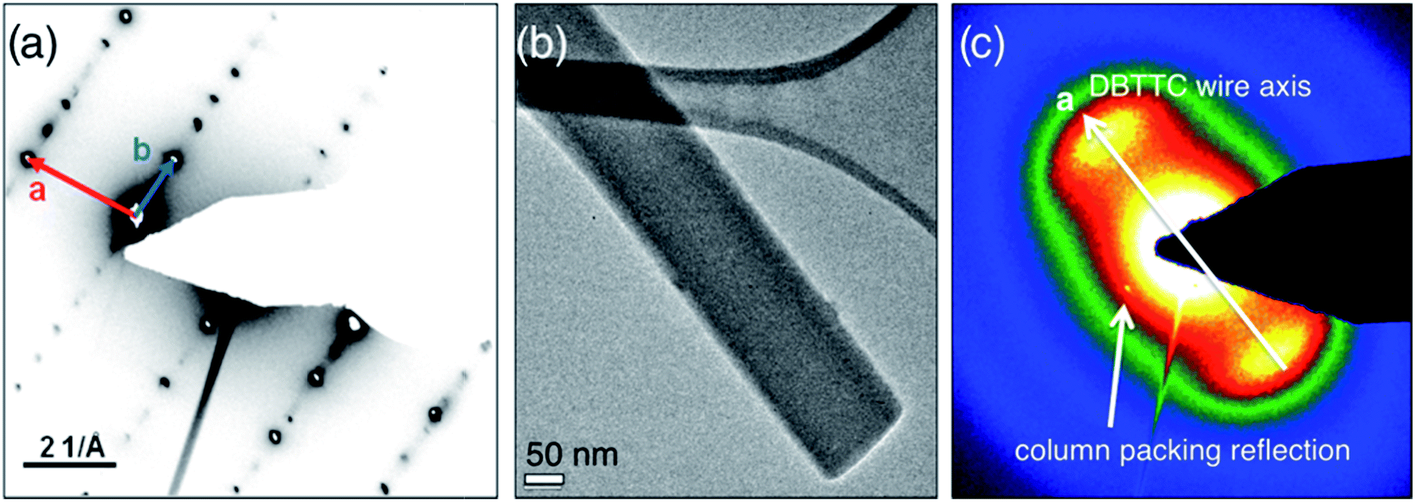 | ||
| Fig. 6 (a) SAED pattern for a single DBTTC nanowire, (b) bright field TEM image and (c) SAED pattern after long exposure of electron beam. | ||
Conclusions
In conclusion, we grew vertical organic nanowire crystals of DBTTC on large-scale graphene with reasonable coverage and uniformity. DBTTC crystals were grown vertically only on graphene film transferred onto SiO2 surface. By measuring AFM and GIXD of DBTTC crystals grown on different surfaces, π–π interaction and surface roughness were found to be the driving force of nanowire growth on graphene surface. On HOPG film, π–π interaction was maximized and DBTTC molecules were spread over HOPG surface due to the lack of surface roughness. GIXD also verified the crystal packing structures and orientation, showing the nanowires consist of well-packed molecular columns with the π-stacking perpendicular to the graphene surface, oriented along the vertical growth axis of the nanopillar crystals. This is noteworthy in that vertical π-stacking with perfect overlap facilitates hole-transport, with great to potential for extensive applications in organic optoelectronics. Long and thin crystals can be used in light-collecting antenna devices; short and dense crystals can be a great bulk-heterojunction photovoltaic cell.Acknowledgements
Research supported as part of the NSF MRSEC program through Columbia in the Center for Precision Assembly of Superstratic and Superatomic Solids (DMR-1420634); this includes. GIXD measurements performed on beamline 11-3 at the Stanford Synchrotron Radiation Laboratory (SSRL), a national user facility operated by Stanford University on behalf of the U.S. Department of Energy, Office of Basic Energy Sciences, and beamline X-9 at the National Synchrotron Light Source (NSLS), Brookhaven National Laboratory, which is supported by the U.S. Department of Energy, Office of Basic Energy Sciences, under Contract No. DE-SC0012704. TEM measurements were also performed at Brookhaven National Laboratory at the Center for Functional Nanomaterials, supported under contract number DE-SC0012704. G. H. L was supported by the Basic Science Research Program (2014R1A1A1004632) through NRF funded by the Ministry of Science, ICT & Future and the Human Resources Program in Energy Technology of the Korea Institute of Energy Technology Evaluation and Planning (KETEP), granted financial resource from the Ministry of Trade, Industry & Energy (No. 20154010200810). K. S. Kim was supported by the Basic Science Research Program through the National Research Foundation of Korea (NRF; grant number: 2014R1A1A1006414) funded by the Ministry of Science, ICT and Future Planning and Priority Research Centers Program (2010-0020207) by the National Research Foundation of Korea (NRF) funded by the Ministry of Education, Science and Technology.Notes and references
- C. Simbrunner, G. Hernandez-Sosa, M. Oehzelt, T. Djuric, I. Salzmann, M. Brinkmann, G. Schwabegger, I. Watzinger, H. Sitter and R. Resel, Phys. Rev. B: Condens. Matter Mater. Phys., 2011, 83, 115443 CrossRef
.
- J. Götzen, S. Lukas, A. Birkner and G. Witte, Surf. Sci., 2011, 605, 577 CrossRef
- T. Breuer and G. Witte, Phys. Rev. B: Condens. Matter Mater. Phys., 2011, 83, 155428 CrossRef
- L. Raimondo, M. Moret, M. Campione, A. Borghesi and A. Sassella, J. Phys. Chem. C, 2011, 115, 5880 CrossRef CAS
- R. R. Nair, A. N. Grigorenko, K. S. Novoslev, T. J. Booth, T. Stauber, N. M. Peres and A. K. Geim, Science, 2008, 320, 1308 CrossRef CAS PubMed
- K. S. Kim, Y. Zhao, H. Jang, S. Y. Lee, J. M. Kim, K. Kim, J. H. Ahn, P. Kim, J. Y. Choi and B. H. Hong, Nature, 2009, 457, 706 CrossRef CAS PubMed
- X. Li, W. Cai, J. An, S. Kim, J. Nah, D. Yang, R. Piner, A. Velamakanni, I. Jung, E. Tutuc, S. K. Banerjee, L. Colombo and R. S. Rouff, Science, 2009, 324, 1312 CrossRef CAS PubMed
- X. Li, Y. Zhu, W. Cai, M. Boryiak, B. Han, D. Chen, R. D. Piner, L. Colombo and R. S. Ruoff, Nano Lett., 2009, 9, 4359 CrossRef CAS PubMed
- K. S. Novoselov, A. K. Geim, S. V. Morozov, D. Jiang, M. I. Katsnelson, I. V. Grigorieva, S. V. Dubonos and A. A. Firsov, Nature, 2005, 438, 197 CrossRef CAS PubMed
- Y. Zhang, Y.-W. Tan, H. L. Stormer and P. Kim, Nature, 2005, 438, 201 CrossRef CAS PubMed
- C.-H. Lee, T. Schiros, E. J. G. Santos, B. Kim, K. G. Yager, S. J. Kang, S. Lee, J. Yu, K. Watanabe, T. Taniguchi, J. Hone, E. Kaxiras, C. Nuckolls and P. Kim, Adv. Mater., 2014, 26, 2812 CrossRef CAS PubMed
- A. K. Geim and I. V. Griogorieva, Nature, 2013, 499, 419 CrossRef CAS PubMed
- L. Zhao, R. He, K. T. Rim, T. Schiros, K. S. Kim, H. Zhou, C. Gutiérrez, S. P. Chockalingam, C. J. Arguello, L. Pálová, D. Nordlund, M. S. Hybertsen, D. R. Reichman, T. F. Heinz, P. Kim, A. Pinczuk, G. W. Flynn and A. N. Pasupathy, Science, 2011, 333, 999 CrossRef CAS PubMed
- T. Schiros, D. Nordlund, L. Pálová, D. Prezzi, L. Zhao, K. S. Kim, U. Wurstbauer, C. Gutiérrez, D. Delongchamp, C. Jaye, D. Fisher, H. Ogasawara, L. G. M. Pettersson, D. R. Reichman, P. Kim, M. S. Hybertsen and A. N. Pasupathy, Nano Lett., 2012, 12, 4025 CrossRef CAS PubMed
- L. Zhao, M. Levendort, S. Goncher, T. Schiros, L. Pálová, A. Zabet-Khosousi, K. T. Rim, C. Gutiérrez, D. Nordlund, C. Jaye, M. S. Hybertson, D. R. Reichman, G. W. Flynn, J. Park and A. N. Pasupathy, Nano Lett., 2013, 13, 4659 CrossRef CAS PubMed
- X. Zhang, T. Schiros, D. Nordlund, Y. C. Shin, J. King, M. Dresselhaus and T. Palacios, Adv. Funct. Mater., 2015, 25, 4163 CrossRef CAS
- M. Cox, A. A. Gorodetsky, B. Kim, K. S. Kim, Z. Jia, P. Kim, C. Nuckolls and I. Kymissis, Appl. Phys. Lett., 2011, 98, 123303 CrossRef
- W. H. Lee, J. Park, S. H. Sim, S. Lim, K. S. Kim, B. H. Hong and K. Cho, J. Am. Chem. Soc., 2011, 133, 4447 CrossRef CAS PubMed
- N. N. Nguyen, S. B. Jo, S. K. Lee, D. H. Sin, B. Kang, H. H. Kim, H. Lee and K. Cho, Nano Lett., 2015, 15, 2474 CrossRef CAS PubMed
- Y. Wang, J. A. Torres, A. Z. Stieg, S. Jiang, M. T. Yeung, Y. Rubin, S. Chaudhuri, X. Duan and R. B. Kaner, ACS Nano, 2015, 9, 9486 CrossRef CAS PubMed
- I. Salzmann, A. Moser, M. Oehzelt, T. Breuer, X. Feng, Z.-Y. Juang, D. Nabok, R. G. Della Valle, S. Duhm, G. Heimel, A. Brillante, E. Venuti, I. Bilotti, C. Christodoulou, J. Frisch, P. Puschnig, C. Draxl, G. Witte, K. Müllen and N. Koch, ACS Nano, 2012, 6, 10874 CrossRef CAS PubMed
- Q. H. Wang and M. C. Hersam, Nat. Chem., 2009, 1, 206 CrossRef CAS PubMed
- C.-Y. Chiu, B. Kim, A. A. Gorodetsky, W. Sattler, S. Wei, A. Sattler, M. Steigerwald and C. Nuckolls, Chem. Sci., 2011, 2, 1480 RSC
- A. A. Gorodetsky, C.-Y. Chiu, T. Schiros, M. Palma, M. Cox, Z. Jia, W. Sattler, I. Kymissis, M. Steigerwald and C. Nuckolls, Angew. Chem., 2010, 122, 8081 CrossRef
- P. Blake, E. W. Hill, A. H. Castro Neto, K. S. Novoslev, D. Jiang, R. Yang, T. J. Booth and A. K. Geim, Appl. Phys. Lett., 2007, 91, 063124 CrossRef
- J. Meyer, V. Scardaci, C. Casiraghi, M. Lazzeri and F. Mauri, Phys. Rev. Lett., 2006, 97, 187401 CrossRef PubMed
- R. A. Laudise, C. Kloc, P. G. Simpkins and T. Siegrist, J. Cryst. Growth, 1998, 187, 449 CrossRef CAS
- K. Xiao, W. Deng, J. K. Keum, M. Yoon, I. V. Vlassiouk, K. W. Clark, A.-P. Li, I. I. Kravchenko, G. Gu, E. A. Payzan, B. G. Sumpter, S. C. Smith, J. F. Browning and D. B. Geohegan, J. Am. Chem. Soc., 2013, 135, 3680 CrossRef CAS PubMed
- S. J. Kang, G.-H. Lee, Y.-J. Yu, Y. Zhao, B. Kim, K. Watanabe, T. Taniguchi, J. Hone, P. Kim and C. Nuckolls, Adv. Mater., 2014, 24, 5157 CAS
Footnotes |
| † Electronic supplementary information (ESI) available: Surface characterization data, details of GIXD data. See DOI: 10.1039/c6ra04742d |
| ‡ These authors equally contributed to this work. |
| This journal is © The Royal Society of Chemistry 2016 |