D. V. M. Paivaa,
M. A. S. Silva
b,
A. S. B. Sombrab and
P. B. A. Fechine*a
aGrupo de Química de Materiais Avançados (GQMAT), Departamento de Química Analítica e Físico-Química, Universidade Federal do Ceará – UFC, Campus do Pici, CP 12100, CEP 60451-970 Fortaleza, CE, Brazil. E-mail: fechine@ufc.br
bLaboratório de Telecomunicações e Ciência e Engenharia de Materiais (LOCEM), Departamento de Física, Universidade Federal do Ceará, Brazil
First published on 25th April 2016
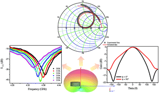
This work reports the dielectric properties of Sr3WO6 (SWO) double perovskite at radio frequencies as a function of the temperature and a study in microwaves range to evaluate the material as a novel dielectric resonator. Thermo-activated charge transfer process for SWO ceramic was observed and two resistor–capacitor associations were fitted for the Nyquist diagram. SWO presented negative values of temperature coefficient of capacitance (TCC) and the activation energies of dielectric relaxation processes were measured by conductivity (1.35 eV), imaginary modulus (1.38 eV) and imaginary impedance (1.36 eV). For the microwave range, SWO shows high dielectric permittivity (13.57) and dielectric loss (0.0281). The dielectric resonator antenna (DRA) fabricated from SWO ceramic presented an operation frequency in 4.1 GHz and return loss below −40 dB. It was possible to evaluate the performance of the antenna from numerical simulation. From these results, the SWO based DRA shows good properties to be used as a novel microwave dielectric resonator.
Sr3WO6 (SWO) is another example of double perovskite that has two Sr2+ ions in site A and one Sr2+ and W6+ ions distributed in the B′ and B′′ sites. SWO presents four polymorphs (α, β, γ and δ) from low to high temperature.10 This material has been traditionally studied due to luminescence properties: the photoluminescence and thermoluminescence properties of Sr3WO6:Eu3+ was reported by Emen and Altinkaya,11 while Zhigang Zou et al.12 obtained an efficient charge compensated red phosphor for Sr3WO6:K+,Eu3+ for white LEDs. However, the SWO perovskite structure are also an important oxide class for dielectric materials with calcium, strontium and barium titanate, the most representative of perovskite structure for dielectric properties.
In this work, the best set of parameters to synthesize the SWO phase by solid-state route was achieved by X-ray diffraction (XRD). The dielectric properties of the material were measured at radio frequency as a function of the temperature (298–718 K). For microwave applications, SWO was experimentally measured as a dielectric resonator and supported by numerical simulation. The results set can be used to suggest potential novel applications for SWO phase as a dielectric resonator antennas (DRA) or other devices that operate in the microwaves range (microwave filters, oscillators, radar detectors etc.).
| 3SrCO3 + WO3 → Sr3WO6 + 3CO2 |
| 3SrCO3 + WO3 → (Sr3WO6)1−x + (SrWO4)x + (SrO)2x + 3CO2 |
The second reaction shows a spurious phase (SrWO4) and SrO (from decomposition of strontium carbonate). This probable reaction was observed for sample synthesized at 1323 K. However, SrO phase was not detected due to the small concentration and weak diffraction peak compared than Sr3WO6 and SrWO4. Thus, it was not taken into account for crystal structure refinement (see XRD results).
The preparation of the samples for dielectric measurements consisted of the fabrication of pellets and a cylindrical ceramic. Thus, SWO powder was molded into a steel die by uniaxial press and its green body sintering at two steps (773 K for 2 h and after at 1523 K for 6 h). The pellets and cylinders were polished after the sintering process. For analysis by Impedance Spectroscopy (IS), both faces of the ceramic pellet were covered with a silver conductive electrode to form a parallel face capacitor geometry. The dimensions of the pellets in dielectric were 14.04 mm of diameter and 7.34 mm of thickness for the microwave range, and 14.30 mm of diameter and 1.56 mm of thickness for the radio frequency range.
The diffractograms were obtained by PANalytical diffractometer (Xpert Pro MPD) operating at 40 kV and 45 mA in the geometry of Bragg–Brentano, with a Cu tube (Kα1 = 1.540562 Å, Kα2 = 1.54439 Å) at room temperature (∼300 K), from crushed samples of SWO in three different temperatures (1323, 1423 and 1523 K). The diffraction patterns were obtained from 15° to 65° (2θ) at a step size of 0.013°, with the analysis time at each step (70 s) in a graphite monochromator and in the plane geometry for diffracted beam. The Rietveld method's13 was used for obtain the refinements through the DBWS Tools software,14 where the refined parameters were the lattice parameters, scale factor, background, U and X parameters, and overall thermal factors. The Inorganic Crystal Structure Database (ICSD) was used to identify what phases were present in the samples.
The IS data (radiofrequency range) were collected in the Solartron 1260 Impedance Analyzer at different temperatures (298–718 K). For this propose, the electric properties of the SWO was represented in terms of the: complex dielectric constant ε*(ω) = ε′ − jε′′, complex impedance Z*(ω) = Z′ − jZ′′, electric conductivity σ*(ω) = 1/Z* = σ′ + jσ′′, electric modulus M*(ω) = 1/ε*(ω) = M′ + jM′′ and loss tangent tan
δ = ε′′/ε′, where (′) and (′′) represents the real and imaginary part, respectively. Where j = ωC0Z* and the vacuum capacitance is represented C0 and j = √−1.15,16 Nyquist diagrams were obtained by fitting using the Eisanalyser software.
The Hakki–Coleman method17,18 was used for dielectric measurements in the microwave range. For antenna applications, the ceramic cylinder was placed in a ground plane (copper sheet). The device was fed by a 50 Ω coaxial cable and SMA connector, as shown in Fig. 1.
Both measurements, by Hakki–Coleman method and by antenna configuration, were undertaken with an Agilent Network Analyser, model N5230A, at room temperature. Using numerical simulations via the High Frequency Structure Simulator (HFSS) of Ansoft, the electromagnetic fields generated by DRA were obtained by simulation of a perfect cylinder model above a perfect ground plane. The air gaps were inserted in the model targeting for approximation of real case between numerical and experimental data from HE11δ mode. Thus, the cylindrical DRA can be approximately by the following equation:
![]() | (1) |
792
458 ms−1), and a (m) is the radius and h (m) is the height of the cylindrical DRA (Fig. 1).
All refinements match with the experimental diffraction profile and there is not significant noise intense in the blue line (Fig. 2). Thus, the refinements were satisfactory, as demonstrate parameters derived from the Rietveld refinement (Table 1), where the lattice parameters, cell volume and density showed no significant changes. One can also observe a small concentration of SrWO4 (6.62% wt) for the sample synthesized at 1323 K. Thus, the phase obtained at 1423 K was chosen for the course of the work due to lower energy involved in the process.
| Sample | Phase | Lattice parameters | Rwp (%) | RBragg | S | Vcell | Quantitative phase analysis (% wt) | Density (g cm−3) | ||
|---|---|---|---|---|---|---|---|---|---|---|
| a (Å) | b (Å) | c (Å) | ||||||||
| SWO (1323 K) | Sr3WO6 | 10.093290 | 17.646570 | 11.813420 | 10.23 | 7.14 | 1.55 | 1714.028 | 93.38 | 6.311 |
| SrWO4 | 5.414999 | 5.414999 | 12.052610 | 8.17 | 353.409 | 6.62 | 6.306 | |||
| SWO (1423 K) | Sr3WO6 | 10.092880 | 17.642370 | 11.814300 | 12.60 | 9.64 | 1.11 | 1713.669 | 100.0 | 6.312 |
| SWO (1523 K) | Sr3WO6 | 10.097800 | 17.649710 | 11.815720 | 12.59 | 8.81 | 1.07 | 1715.148 | 100.0 | 6.307 |
Complex impedance spectroscopy (CIS) technique was used for analyzing the electric response of SWO ceramic under influence of the variation of frequency as a function of the temperature, and investigate the dielectric behavior. By measurements of CIS is possible find the phase transitions of the materials. In this sense, dielectric permittivity (ε′) was measured at 1 MHz and plotted as a function of the temperature (Fig. 3). It can be seen a maximum value for ε′ at 445 K, corresponding to the transition temperature observed in literature,21,22 where the SWO transits of triclinic for monoclinic symmetry, i.e., the γ ↔ β phase transition. King and coworkers10 observed the same phenomena by using electron diffraction, synchrotron X-ray powder diffraction and neutron powder diffraction.
![]() | ||
| Fig. 3 Dielectric permittivity (ε′) measured at 1 MHz as a function of the temperature and the representative picture of phase transition (inset). | ||
The dielectric characterization in the radiofrequency region as a function of the temperature (298–718 K) was used to investigate the changes in the dielectric behavior of the material. Fig. 4(a) and (c) present the ε′ profile and show two behavior before and after the transition temperature (445 K). Before the phase transition, ε′ values presented a decrease behavior when the temperature increases, as demonstrated by values of temperature coefficient of capacitance (TCC). This behavior is probably due to the triclinic SWO, where negatives values were obtained (Table 2). After transition temperature, the dielectric permittivity increases proportionally with the temperature. In this case, positive values of TCC can be obtained and shows the characteristics of monoclinic SWO. These values can be explained by increasing of polarization with the change of symmetry of SWO with increasing of temperature, where the highest temperature promotes a higher polarization23 or increasing of conductivity due to the mechanism of conduction activated by temperature. The tan
δ profile (Fig. 4(b) and (d)) presents similar behavior when compared to ε′ values.
![]() | ||
Fig. 4 Dielectric spectra at 298–718 K: (a) and (c) for constant (ε′); and (b) and (d) for dielectric loss (tan δ). | ||
| Frequency (Hz) | TCC (ppm °C−1) |
|---|---|
| 100 | −6156.52 |
| 1k | −4474.66 |
| 100k | −1539.27 |
| 1 M | −471.73 |
Some process activated by temperature are analyzed by shift of maximum frequency in the M′′(f), ε′′(f), Z′′(f) diagrams or by conductivity with temperature variation. Fig. 5(a)–(c) show measurements of conductivity (σ′ac), imaginary modulus (M′′) and imaginary impedance (Z′′) as a function of the temperature (after phase transition, 608–718 K). The activation energy (Ea) for this thermo-activated process was calculated by shifting frequency of maximum frequency and the values for this thermo-active process were about 1.3 eV. Some double perovskites present smaller values than SWO, as La2Co1+x(MgyTi1−y)1−xO6 (Ea = 0.77–0.81 eV),24 BaPrCoTaO6 (Ea = 0.35–0.38 eV),25 BaLaMnSbO6 (Ea = 0.49–0.51 eV),26 Sr2CeTaO6 (Ea = 0.78 eV),27 BaPrCoNbO6 (Ea = 0.4 eV)28 and Sr2MgMoO6−δ (Ea = 0.52 and 1.43 eV).29 Therefore, the thermo-active process requires more energy for SWO. The analysis of the Ea by three different methods showed values very close to each other and they are indicate of the same phenomenon.
![]() | ||
| Fig. 5 Ea obtained by temperature shift: (a) conductivity, (b) imaginary electric modulus and (c) imaginary impedance. | ||
The global dielectric and electric properties in the ceramic may be sum of contributions as electric and/or dielectric response provide by grain, grain boundary or electrode. The analysis of Nyquist diagram enables the visualization of this contribution. This model can be seen by fitting with equivalent circuit method or by models (Cole–Cole, Cole-Davidson etc.) or by well defined semi-circle. The impedance measurements showed the presence of semicircle, where these results were fitted by equivalent circuit model. Although of this results show only one semicircle, it was necessary to use two associated RC for best fitting. Fig. 6(a) demonstrates the experimental and obtained Nyquist diagram following this methodology. The fittings presents good correlation with experimental data. Fig. 6(b) shows the equivalent circuit for SWO, where it can be seen two resistor–capacitor (RC) circuit. They are associated with the grain (Cg and Rg) and grain boundary (Cgb and Rgb) of the ceramics. In these associations were utilized Constant Phase Element (CPE) instead of capacitance and it is well justified by increasing of conductivity of ceramic with temperature and the impedance values decreasing with temperature. Table 3 summarizes the fitting value of parameters used in equivalent circuit. The R, P and N parameters were obtained by fitting and presents different values, dependent on the temperature. For example, the resistances R1 and R2 decrease when the temperature increase due to the increased conductivity. However, the N parameter decreased with temperature, since the material becomes more conductive and the capacitive characteristic ceases. The parameter are marked by subscript numbers 1 and 2. They are assigned to grain and grain boundary parameters, respectively.
| T (K) | Grain | Grain boundary | ||||
|---|---|---|---|---|---|---|
| R1 (Ω) | P1 | N1 | R2 (Ω) | P2 | N2 | |
| 608 | 2.71 × 10⁶ | 9.32 × 10⁻⁸ | 0.692 | 2.50 × 10⁷ | 8.26 × 10⁻¹¹ | 0.883 |
| 618 | 2.26 × 10⁶ | 7.61 × 10⁻⁸ | 0.563 | 1.59 × 10⁷ | 8.39 × 10⁻¹¹ | 0.888 |
| 628 | 1.30 × 10⁶ | 9.56 × 10⁻⁸ | 0.645 | 1.05 × 10⁷ | 8.13 × 10⁻¹¹ | 0.896 |
| 638 | 1.17 × 10⁶ | 2.64 × 10⁻⁷ | 0.453 | 6.97 × 10⁶ | 8.41 × 10⁻¹¹ | 0.897 |
| 648 | 5.57 × 10⁵ | 1.80 × 10⁻⁷ | 0.620 | 4.73 × 10⁶ | 1.00 × 10⁻¹⁰ | 0.884 |
| 658 | 3.49 × 10⁵ | 3.30 × 10⁻⁷ | 0.579 | 3.08 × 10⁶ | 1.07 × 10⁻¹⁰ | 0.882 |
| 668 | 2.07 × 10⁵ | 5.02 × 10⁻⁷ | 0.602 | 2.07 × 10⁶ | 1.17 × 10⁻¹⁰ | 0.877 |
| 678 | 1.42 × 10⁵ | 6.60 × 10⁻⁷ | 0.569 | 1.45 × 10⁶ | 1.20 × 10⁻¹⁰ | 0.878 |
| 688 | 9.96 × 10⁴ | 1.12 × 10⁻⁶ | 0.514 | 1.07 × 10⁶ | 1.32 × 10⁻¹⁰ | 0.875 |
| 698 | 6.83 × 10⁴ | 1.45 × 10⁻⁶ | 0.534 | 8.10 × 10⁵ | 1.53 × 10⁻¹⁰ | 0.867 |
| 708 | 4.83 × 10⁴ | 2.68 × 10⁻⁶ | 0.524 | 6.54 × 10⁵ | 1.33 × 10⁻¹⁰ | 0.877 |
| 718 | 3.85 × 10⁴ | 3.35 × 10⁻⁶ | 0.498 | 5.62 × 10⁵ | 1.00 × 10⁻¹⁰ | 0.895 |
In microwaves range (7.84 GHz), the SWO shows high dielectric permittivity (ε′ = 13.57) and dielectric loss (tan
δ = 0.0281). This dielectric characterization was performed by Hakki–Coleman method, where was analyzed the TE011 mode of the cylindrical resonator. The dielectric properties demonstrated good agreement with results obtained in IS.
The temperature coefficient of resonant frequency (τf) for SWO, i.e., the dielectric properties variation with increasing temperature was measured by the SFS method.30 The τf was measured by monitoring of displacement mode HE11δ frequency with increasing of temperature (Fig. 7(a)) and the linear correlation of temperature and HE11δ frequency was observed (Fig. 7(b)). It was possible observed that with the increase of temperature the mode fHE11δ shifts to smaller frequency. The linear fit with the experimental points were used to calculate τf (−207.60 ppm K−1). SWO shows an improbable τf values when compared to the results from other materials, where in the literature other double perovskites presented values below 25 ppm K−1.1,31–35
![]() | ||
| Fig. 7 (a) Displacement of mode fHE11δ with variation of temperature and (b) temperature coefficient of resonant frequency (τf) of SWO. | ||
For the microwave applications, SWO dielectric resonator was analyzed in the antenna setup (Fig. 1). From this experiment was possible to obtain the main parameter for evaluating the antenna device: return loss (S11), bandwidth and by numerical simulation in HFSS® software. The far field parameters were also obtained as radiation patterns, gain and efficiency of antenna. For the first analysis, the return loss (Fig. 8(a)) presented by SWO-based DRA shows operation frequency (fHE11δ) in 4.12 GHz and return loss (−43.96 dB) below −10 dB, and presents a good coupling and operating as an antenna (error = 0.75%), as shown in Table 4. Fig. 7 also shows a good agreement between experimental and simulated return loss obtained by numerical simulation and collected data. This condition is necessary for acquisition of accurate far field's parameters.
| SWO-based DRA | |||
|---|---|---|---|
| Experimental | Simulated | Error (%) | |
| fHE11δ | 4.1256 | 4.1260 | 0.010 |
| S11 (dB) | −43.97 | −43.64 | 0.753 |
| BW (%) | 7.268 | 7.053 | 2.958 |
| Efficiency (%) | 57.90 | ||
| Peak resonant resistance (Ω) | 108.125 | 107.155 | 0.896 |
| Resistance (Ω) | 49.702 | 50.280 | 1.163 |
| Directivity (dBi) | 3.41 | ||
| Gain (dBi) | 1.98 | ||
For validation of the numerical simulation, it is necessary a good agreement of return loss and impedances or Smith chart with experimental data. Fig. 8(b) shows experimental and simulated Smith chart. Both presents inductive characteristics and the simulated results presents minor deviations from experimental data. Table 4 summarizes the results obtained by simulations and experimental data, where the DRA presents a bandwidth of 7% or 287 MHz. These results are consistent for DRA characteristics. The gain (1.98 dBi) and efficiency (57.90%) obtained in simulation shows small values compared with another DRAs in the literature.20,36–39 However, these parameters can be improved by a better coupling between DRA and SMA probe in the antenna device. The radiation profile of DRA is showed in the Fig. 9. One can observed the cylindrical dielectric resonator involved by a simulated radiation patterns. The inset of the Fig. 9 shows that the radiation pattern profile is consistent with a cylindrical DRA, with maximum radiation for θ = 0° when analyzed by φ = 90° and φ = 0°.
These results shows an antenna device with a good gain and an appreciable efficiency operating at 4.12 GHz. In this sense, to create a device available for Wi-Fi devices (5.15–5.875 GHz)40 using SWO-based DRA, for example, requires a miniaturization process of this antenna, once the fHE11δ is a function of dimensions and dielectric properties (see eqn (1)). The better coupling of this novel resonator with the coaxial feed presents gain values closer of commercial antennas (2–3 dBi for residential users). In addition, due to isolating characteristics (higher Ea and impedance (Z > 1 GΩ)), higher stable dielectric (200 < TCC −5600 ppm °C−1) and low dielectric permittivity, the SWO ceramic also can be applied in devices than needs of dielectric class 1.41,42
| This journal is © The Royal Society of Chemistry 2016 |