Jheng-Yuan Syuab,
Yu-Min Chenb,
Kai-Xiang Xub,
Shih-Ming Hea,
Wu-Ching Hungc,
Chien-Liang Changc and
Ching-Yuan Su*abd
aGraduate Institute of Energy Engineering, National Central University, Tao-Yuan 32001, Taiwan. E-mail: cysu@ncu.edu.tw
bDep. of Mechanical Engineering, National Central University, Tao-Yuan 32001, Taiwan
cNational Chung-Shan Institute of Science and Technology, Tao-Yuan, Taiwan
dGraduate Institute of Material Science and Engineering, National Central University, Tao-Yuan 32001, Taiwan
First published on 28th March 2016
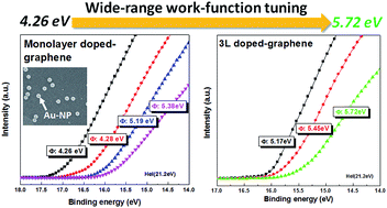
Graphene is regarded as a potential candidate to replace the transparent conductive (TC) electrodes that are currently used in various optoelectronic applications. However, there is still a lack of methods by which to achieve low sheet resistance (Rs) with stable doping and work functions with a wide range of tunability, which is significant for band alignment at the interface to enhance charge transport and thus to achieve higher device performance. We developed a novel strategy for preparing a TC electrode by doping layer-by-layer (LBL)-stacked graphene with AuCl3, by which means an excellent TC performance (an Rs of 40 ohm sq−1 at a transmittance (T) of 89.5%) and an extremely wide range of work-function tunability (∼1.5 eV) were successfully achieved. Moreover, a hybrid electrode prepared by transferring doped graphene onto a pre-patterned Cu metal mesh exhibited a low resistance of ∼4.9 ohm sq−1. In addition, we monitored the long-term stability of AuCl3-doped graphene for 6 months and also constructed a model for accelerated degradation testing. The relevant mechanism of charge transfer between the graphene and the dopants was characterized based on X-ray photoelectron spectroscopy (XPS) spectra to elucidate degradation observed after long-term testing. This work contributes a novel type of “active electrode”; the doped graphene film not only serves as a high-performance TC electrode but also provides a wide range of tunable work functions. The proposed active electrode is prepared using a scalable and facile doping process, which paves the way for its usage in applications such as optoelectronic devices.
A graphene-based TC film can be synthesized using various methods, including methods based on solution-processed reduced graphene oxide (rGO),7–9 liquid-phase exfoliation10 and electrochemically exfoliated graphene flakes;11,12 in this last case, the graphene flakes can be easily dispersed to form a suspension ink, from which a thin film can then be obtained via versatile coating routes, such as Langmuir–Blodgett (LB) assembly,13,14 spray coating15 and rod coating.16 Although these methods have the advantages of low cost and scalable production, the high resistance (approximately a few to a few thousand kohm sq−1) of the films they produce still hinders their usage. Alternatively, in recent efforts, large-area and high-quality graphene films have been successfully achieved via chemical vapor deposition (CVD).17–21 CVD-grown graphene exhibits scalability and high conductivity as well as controllable transparency; as a result, CVD growth is considered to be a promising route by which to obtain graphene TC electrodes. The typical sheet resistance of intrinsic monolayer graphene ranges from ∼1 kohm sq−1 to 5 kohm sq−1.20,21 The layer-by-layer (LBL) stacking of up to four layers of graphene film improves this resistance to ∼350 ohm sq−1 while maintaining a transparency of greater than 90%.22 However, this improved sheet resistance is still inferior to the sheet resistance of ITO. To reduce the sheet resistance of CVD-grown graphene, various methods have recently been employed to obtain p-doped graphene with acid, molecular and AuCl3 precursor,23–27 in which the transfer of charge (electrons) from the graphene to the dopants significantly increases the hole carrier concentration of the graphene, leading to remarkably lower sheet resistance. For example, four layer (4L)-stacked graphene with nitric acid doping exhibits a low sheet resistance of 30 ohm sq−1 (T ∼ 90%).18 LBL doping with AuCl3 also results in high performance, with a sheet resistance of 54 ohm sq−1 (T ∼ 85%).27 Moreover, it has been reported that AuCl3-doped graphene exhibits higher stability than graphene with other reported dopants because most other dopants readily desorb from the graphene during long-term operation, thereby degrading its stability.
Current electronics and optoelectronics require a so-called “active electrode” with an appropriate work function (WF) to achieve band-structure alignment at the interface, enhancing the efficiency of carrier transport and thus yielding higher device performance. Therefore, the discovery of a new type of electrode with a wide range of work-function tunability would be beneficial for the development of various optoelectronic devices. Typical transparent oxide electrodes, such as ITO, exhibit limited WF tunability (∼0.5 eV) because the Fermi level becomes pinned once the ITO film has been deposited onto a specific substrate. Graphene has been exploited as a novel active electrode in this regard because its high transparency, charge mobility and flexibility make it a promising candidate for application in many bendable optoelectronics, such as organic photovoltaics (OPVs),26,28,29 organic electronics,30,31 and OLEDs.32 Various approaches have been reported for altering the WF of graphene, including molecular and chemical functionalization,33–35 metal contact doping,36,37 and the intercalation of lithium, fluorine, or iron chloride into few-layer graphene.38–40 However, the surface functionalization of graphene often destroys the intrinsic graphene lattice, thereby severely degrading its conductivity and charge mobility.41 Recently, doping with Au precursors (AuCl3, HAuCl4, Au(OH)3, etc.) has been demonstrated to enable the stable modulation of the graphene WF because the as-formed Au nanoparticles (Au-NPs) decorated on the graphene allow charge-transfer doping with long-term stability.23,24,27,42–45 A configuration with LBL Au precursor doping on stacked graphene films has been reported to exhibit higher performance in terms of both electrical and optical properties.27,45 Moreover, this doping technique allows graphene to maintain its high conductivity and transparency during long-term operation. However, the modulated WFs that can be achieved using most reported methods based on the doping of graphene span only a limited range of approximately 0.5–1.0 eV, and precise control of the graphene WF has yet to be demonstrated.34,46
In this study, we propose a novel approach for preparing graphene-based TC films with a remarkably wide range of work-function tunability (up to ∼1.5 eV). To realize this novel type of film, we perform the LBL stacking of high-quality CVD-grown graphene to form a transparent electrode, followed by a doping process. Several dopants for graphene films, such as TFSA (tetrafluorosuccinic acid, C4H2F4O4), PBASE (1-pyrenebutyric acid N-hydroxysuccinimide ester, C24H19NO4), HI (hydroiodic acid) and AuCl3 precursor, were comprehensively studied and compared. The AuCl3 doping was optimized under various conditions, resulting in excellent optical and electrical performance (Rs ∼ 40 at T > 89%). The morphology of the Au-decorated graphene was characterized using an electron microscope, revealing the various shapes of the nanostructures. The WFs of the doped graphene electrodes were estimated using ultraviolet photoelectron spectroscopy (UPS) and found to span a wide range, from 4.26 to 5.72 eV. Long-term stability testing for up to 6 months was performed to evaluate the doping stability. Most importantly, the AuCl3 doping mechanism was investigated in detail via the X-ray photoelectron spectroscopy (XPS) characterization of the chemical bonding status. Moreover, a novel hybrid electrode consisting of a pre-patterned Cu micro-mesh and a doped LBL graphene film was fabricated to improve the electrical conductivity of this novel transparent electrode.
To study the doping effect in monolayer graphene, AuCl3 doping at various concentrations (10, 20, and 30 mM) was performed. Fig. 2a shows the UV-vis absorption spectra for samples at various concentrations. The optical transparency at 550 nm was greater than 95% for all samples. In addition, as shown in Fig. 2b, the sheet resistances of otherwise identical graphene samples exhibited remarkable decreases of up to 90.6% with AuCl3 doping, from 1.3 kohm sq−1 for the pristine graphene to ∼121.9 ohm sq−1 for the 30 mM AuCl3-doped graphene. The optical transparencies and sheet resistances of 1L graphene with the other doping agents, TFSA, PBASE and HI, are shown in Fig. S3.† The optimized conditions for each case are summarized in Fig. 2c for comparison; this figure indicates that the doping of the graphene with 20 mM AuCl3 resulted in the highest performance of the resulting transparent electrode compared with the other doping methods. Although HI-treated samples were expected to lower the sheet resistance due to strong electron affinity of iodine atom on graphene, leading to hole-doping. It is noteworthy that the HI-treated samples did not exhibit obvious sheet resistance reduction (Fig. 2c and S3†). This could be attributed to low adsorption stability of iodine on graphene as been studied in previous report,53 indicating extremely low bonding energy of C–I. As such, the dopants induced p-type doping on graphene was limited.
To understand the Au ion doping mechanism underlying this phenomenon, XPS measurements were performed. Fig. 2d shows the Au 4f core-level spectra for 1L graphene films doped with various concentrations of AuCl3, in which the peaks near 90.3 and 86.6 eV are assigned to the Au ion (Au3+) and the peak near 84.1 eV is assigned to neutral Au (Au0).54 The Au0 intensity, as indicated in Fig. 2d, increased along with the doping concentration (i.e., in the sequence 10 mM < 20 mM < 30 mM); this result is ascribed to the reduction of the Au ion to natural Au as a result of its acceptance of a large number of electrons from the graphene. In addition to the electron transfer, the AuCl3 could also be decomposed and reduced to Au0 when it is exposed to light or under heat. It has been reported that AuCl3, on carbon nanotube, starting transfer to Au0 at about 200 °C due to the evaporation of Cl2.55 As such, the thermal treatment (∼120 °C) carried out in this study is considered as another reduction factor. Fig. 3 shows the surface morphologies as observed via SEM for AuCl3-doped graphene samples with various AuCl3 precursor concentrations. The Au nanostructure was found to be uniformly distributed on the graphene surface at 10 mM and 20 mM (see (a) and (b), respectively); however, segregation occurred at a concentration of 30 mM (as shown in (c)), indicating that the doping concentration should be optimized to prevent severe metal particle aggregation. Note that different concentrations led to different shapes of the Au nanostructures; for example, Au-NPs with an average diameter of 23 nm were observed with 10 mM doping, as shown in (g). At 20 mM, in addition to Au-NPs, a large number of triangle-shaped Au nanoplates (size: ∼50 μm) began to form, as shown in (e) and (h). When the precursor concentration was increased to 30 mM, the size of the Au plates increased to greater than 150 μm; moreover, Au nanorods began to form. The formation of isotropic Au nanostructures, such as that of Au-NPs, occurs through thermodynamic means (i.e., homogeneous nucleation and subsequent growth of the nuclei), whereas for anisotropic Au nanostructures, such as nanorods and nanoplates, the formation mechanism is a seed-mediated growth process.56 Alternatively, a recent report indicates that the graphene itself can induce the transformation of the material structure; for example, the transformation of fcc-Au to hcp-Au was observed when Au ions were precipitated onto a graphene surface.57 In addition, Au-NPs were found to preferentially segregate to and decorate the cracked and wrinkled regions of the graphene film (see Fig. 3d); these Au-NPs could spontaneously fill in the cracked regions, which is believed to have reduced the degradation of the electrical conductivity during the transfer process.
Because doping with a high concentration (i.e., greater than 30 mM) of AuCl3 resulted in severe aggregation, in the subsequent experiment, we selected a concentration of 20 mM for the doping of the graphene film. To investigate the effect of doping on LBL-stacked graphene films, films with different numbers of graphene layers were characterized in terms of their optical transmittance and sheet resistance (Fig. 4a and b). The compiled data are listed in Table 1; the sheet resistance gradually decreased to 40.1 ohm sq−1 with the addition of further graphene layers, and the transmittance remained at >89.5%, indicating that the decoration of graphene with Au-NPs facilitates high electrical conductivity and ultra-low light absorption. These results are superior to those for pristine graphene and comparable to those for currently available ITO electrodes.
No. of layers | Pristine graphene | LBL graphene doped with AuCl3 (20 mM) | |||||
---|---|---|---|---|---|---|---|
T (%) | Rs (ohm sq−1) | Raman G peak position (cm−1) | T (%) | Rs (ohm sq−1) | Raman G peak position (cm−1) | Carrier concentration (cm−2) | |
1 | 97.38 | 1302.5 | 1582.2 | 95.77 | 127.59 | 1596.6 | 4.17 × 10¹³ |
2 | 95.75 | 865.89 | 1574.8 | 93.91 | 76.56 | 1592.5 | 6.14 × 10¹³ |
3 | 93.51 | 692.78 | 1572.3 | 92.10 | 70.56 | 1590.5 | 7.98 × 10¹³ |
4 | 91.04 | 497.55 | 1571.9 | 89.51 | 40.11 | 1588 | 1.24 × 10¹⁴ |
To further study the effect of doping, Raman spectroscopy was performed on doped graphene films. It has been reported that the position shift of the G peak is sensitive to doping because of the phonon-stiffening phenomenon that occurs via charge transfer.54 The spectroscopic features of the G peak are associated with the degree of p-type doping of graphene; a more prominent upward shift of the G peak is observed with increasing p-type doping. Therefore, the doping degree is more strongly correlated with the G-peak shift (with respect to pristine graphene) than with the G-peak position.53 In this study, the Raman spectra revealed a slight downward shift of the G peak with an increasing number of graphene layers at the same doping concentration (Fig. 4c). By contrast, the doped graphene exhibited a significant upward shift compared with the pristine graphene with the same number of layers (Fig. 4d); the G peak was shifted upward by 16.6 cm−1 from 1571.8 (pristine graphene) to 1588.4 cm−1 (doped graphene) in the case of 4L graphene, which was more prominent than the 14.4 cm−1 shift observed for 1L graphene. As mentioned previously, the Au ions were spontaneously reduced to neutral Au particles through the acceptance of electrons from the graphene, leading to heavy p-type doping because this charge-transfer process withdraws electrons from the graphene, thus leaving behind a large number of hole carriers. The same tendency was observed in 3L graphene samples with different precursor concentrations (Fig. S4†), for which the 2D peak showed a slight shift, whereas the G peak was shifted by ∼30 cm−1 with the increase in the doping concentration from 10 to 30 mM.
The mechanism of doping-induced charge transfer was investigated by measuring the carrier concentrations of the doped graphene. Fig. 6a shows the evolution of the carrier concentration from pristine graphene to doped and stacked graphene, where the hole carrier concentration exhibits an increase of approximately two orders of magnitude, from 1.82 × 1012 cm−2 (1L pristine graphene) to 1.24 × 1014 cm−2 (4L doped graphene). Note that heavy p-doping of graphene can alter the electronic structure of the graphene by shifting the Fermi level closer to the valence band, resulting in a change in the WF. Fig. 5b and c show the UPS spectra near the secondary electron threshold for 1L (Fig. 5b) and 3L (Fig. 5c) graphene at various concentrations of AuCl3 doping. The WF ϕ can be extracted from the following equation: ϕ = hν − (Ef − Ecut-off), where hν and Ef are the excitation photon energy (21.2 eV) and the Fermi level edge (0 eV, as shown in the full spectra presented in Fig. S5†), respectively. Here, the value of Ecutoff is determined based on the linear extrapolation and x intercept of the binding energy obtained from the UPS spectra. The extracted WFs are indicated in Fig. 5b and c, showing that the value could be gradually altered over an ultra-wide range of 1.46 eV, from 4.26 eV (pristine 1L graphene) to 5.72 eV (doped 3L graphene). To the best of our knowledge,23,34,54 this represents the widest reported tuning range for a transparent graphene electrode, which allows this novel method to be used to realize the aforementioned active electrodes required for versatile applications in optical electronics.
For certain specific applications, transparent electrodes are required to be durable and suitable for long-term operation. Most reported doping technologies, including doping with Au ions (AuCl3 or HAuCl2), suffer from degradation and a lack of stability testing. Fig. 6 presents the results of monitoring the long-term stability (in an air atmosphere at room temperature) of a doped 3L graphene sample, the sheet resistance of which instantly dropped to 76.2 ohm sq−1 upon doping and then gradually increased to 316.8 ohm sq−1 after three months (see Fig. 6a). Accelerated degradation tests were also performed by heating the sample to 80 °C and 140 °C; in these tests, the sheet resistance rapidly increased to 255.9 (80 °C) and 315.2 ohm sq−1 (140 °C) after 180 min (see Fig. 6b). The results indicate that 140 °C heating can accelerate degradation analogous to that observed over 3 months of room-temperature operation. Therefore, these conditions were adopted as a baseline for the accelerated degradation testing of Au-ion-doped graphene.
Moreover, to detail the mechanism of this degradation, the XPS spectra of carbon 1s (C 1s) and chloride 2p (Cl 2p) were measured to understand the chemical bonding status before and after heat treatment. Fig. 7a shows the XPS C 1s spectra of the doped graphene before and after thermal treatment at 140 °C for 180 min, in which the peaks at ∼284.5 eV and 287 eV correspond to the CC (sp2) and C–Cl bonds, respectively (refer to Fig. S7† for the XPS survey spectrum). Clearly, the ratio of the integrated area of the C–Cl peak to that of the C
C peak decreased from 0.79 for the initial doped graphene sample to 0.49 for the sample subjected to thermal treatment, indicating that the thermal treatment induced the decomposition of the C–Cl bond. Another key observation is the significant reduction in the intensities of the peaks associated with Cl-2p2/3 (at ∼198.7 eV) and Cl-2p1/2 (at ∼199.8 eV) in the Cl(2p) spectra (Fig. 7b), implying the loss of Cl from the doped graphene. The XPS results suggest that AuCl3 doping can immediately lead to significant p-type doping due to the withdrawal of electrons from the graphene through Cl ion adsorption and C–Cl bonding, in addition to the aforementioned Au ion reduction. The subsequent long-term exposure or thermal treatment of the doped graphene results in Cl ion desorption and the decomposition of the C–Cl bond, leading to lower p-type doping of the graphene and thus gradually increasing the sheet resistance.
Recently, the use of TC electrodes based on metal meshes, such as those made of copper and silver, has become a mainstream strategy in the industry in addition to ITO. Recent works have proposed hybrid electrodes fabricated by combining graphene with nanowires or printable metal meshes, which results in a lower sheet resistance because the fine metal wire provides efficient charge carrier transport while the graphene fully covers the interspaces of the mesh and enhances carrier collection without degrading its transparency.58 Such a hybrid electrode structure compensates for the high sheet resistance of pristine graphene, allowing the sheet resistance to be improved by more than 3 orders of magnitude with little degradation in transmission. In addition, because of the excellent water/gas anti-permeability properties of graphene, the graphene film covering the metal mesh can significantly suppress its oxidation. To obtain a high-performance transparent electrode, this novel strategy of combining a Cu metal mesh with a doped monolayer graphene was implemented by transferring a doped 1L graphene film onto the top of a pre-patterned Cu mesh (with a grid width of 10, 30, or 50 μm) on a glass substrate, as shown in Fig. 8a–c. Fig. S6† shows that the transmittance was decreased by ∼2% when the 1L graphene fully covered the Cu mesh. The sheet resistance was found to be further improved to approximately 37.5, 15.0 and 4.9 ohm sq−1 at transparency levels of 82.1, 72.7, and 62.7%, respectively (Fig. 8d). The correlations between the sheet resistance and the transmittance achieved using the various doping technologies considered in this report are summarized in Fig. 8e, and the results suggest that AuCl3-doped 3L graphene or a hybrid electrode prepared by combining such a film with a metal mesh can yield the highest performance among all of the investigated graphene-based TC electrodes.
We used four different dopants in this study: (1) TFSA dissolved in CH3NO2, (2) PBASE dissolved in DMF, (3) AuCl3 in CH3NO2, and (4) HI vapor. The concentrations of TFSA in CH3NO2 were 1, 10, 20, 50, and 100 mM; the concentrations of PBASE in DMF were 1, 5, and 10 mM; and the concentrations of AuCl3 in CH3NO2 were 10, 20, and 30 mM. For HI vapor doping, the graphene samples were treated with HI (57%) vapor at 120 °C for 1 h.
To fabricate the hybrid transparent electrodes consisting of Cu metal mesh and doped graphene film, metal meshes with different grid line widths of 10, 30, and 50 μm were produced via photolithography. The detailed procedure included the following steps: (1) spin coating the positive photoresist (SPR-220, Dow) in two steps, at 1000 rpm for 10 s and then at 3000 rpm for 30 s; (2) baking at 120 °C for 90 s; (3) exposure to UV light for 45 s; (4) developing the pattern with a developer (MF-319, Dow) and then cleaning the residue with DI water, followed by drying with nitrogen gas; (5) depositing Cu (50 nm)/Ti (50 nm) via electron beam evaporation; and (6) removing the unwanted pattern via a lift-off process using acetone and IPA.
Footnote |
† Electronic supplementary information (ESI) available: The detailed procedures for the CVD growth of graphene and the transfer process; XPS, Raman and UPS spectra for doped graphene are available. See DOI: 10.1039/c6ra04449b |
This journal is © The Royal Society of Chemistry 2016 |