
Novel TiO2/Sb2S3 heterojunction with whole visible-light response for photoelectrochemical water splitting reactions†
Yung-Tao Song‡
,
Lu-Yin Lin‡*,
Yu-Shiang Chen,
Hong-Qin Chen,
Zong-De Ni,
Chao-Chi Tu and
Sheng-Sian Yang
Department of Chemical Engineering and Biotechnology, National Taipei University of Technology, 1 Sec. 3, Zhongxiao E. Rd., Taipei 10608, Taiwan. E-mail: lylin@ntut.edu.tw; Fax: +886-2-2731-7117; Tel: +886-2-2771-2171 ext. 2535
First published on 10th May 2016
Abstract
Artificial photosynthesis represents a direct approach toward addressing energy and environmental issues by producing fuels such as hydrogen that can be used in fuel cells. Under the framework of Z-scheme water splitting, we develop a composite TiO2 nanorod/Sb2S3 nanooctahedron photoanode, which possesses low onset potential and high photocurrent density. In this work, to mitigate the poor visible light absorption and low quantum efficiency of TiO2, the concept of n/n heterojunction is introduced by using a composite composed of an additional n-type semiconductor and coating it on n-type TiO2 nanorods. A stibnite Sb2S3 is selected as the coating material due to its suitable band-edge position and visible-light response. A photocurrent density of 0.79 mA cm−2 (measured at 1.23 V vs. RHE) and onset potential of −0.08 V vs. RHE are obtained for the photoanode with the TiO2 nanorod/Sb2S3 nanooctahedron structure in a 0.5 M Na2SO4 aqueous solution under AM 1.5G illumination. This successful combination of two n-type semiconductors provides a conceptual blueprint for material and conduction/valence band design as attractive catalysts for the photoelectrochemical water splitting reaction.
1. Introduction
Artificial photosynthesis has been considered to be a desirable approach for supplying clean energy by capturing and storing the energy of sunlight into the chemical bonds of fuels such as hydrogen. This solar-to-fuel conversion process originated from the demonstration of photoelectrochemical water splitting using n-type TiO2 by Honda and Fujishima in 1972.1 Since then, the photoanodic properties of TiO2 have been widely studied. TiO2 is well-known as a candidate for photoelectrochemical water splitting reactions due to its high photocatalytic activity as well as its abundant and stable properties in an aqueous solution under irradiation.2 However, the large band gap (∼3.0 eV for rutile) makes it only active in the ultraviolet (UV) region which contributes less than 5% of the total energy of the solar spectrum,3 and the low electron mobility (1 cm2 V−1 s−1)4 as well as the short minority carrier (hole) diffusion length (10–100 nm)2,5 limit the quantum efficiency of TiO2 even in the UV region. Improving electron–hole separation by increasing the charge transfer and kinetics of photoelectrochemical water splitting reactions by holes as well as extending the absorption of TiO2 are prerequisites to enhancing the solar energy conversion efficiency of TiO2. Formation of composites with heterojunction interfaces between components with matching band potentials can create a type-II electronic architecture to localize electron and hole wavefunctions in the core or shell material, thereby extending exciton lifetimes,6–8 and some visible absorption may be brought in with the combined material.8–10Recently, efforts have been devoted to the formation of heterojunction between TiO2 and narrow band gap semiconductors to develop highly active photocatalysts that respond under visible light. These research directions include enhanced or tunable light absorption and improvement of photo-generated electron–hole separation as well as an enhancement of the interfacial charge transfer efficiency.7,9,11,12 Smith et al. have designed WO3/TiO2 and TiO2/WO3 quasi-core–shell nanorod (NR) arrays with beneficial optical, chemical, and transport properties of both materials.7 Ke et al. obtained much higher photoactivity in the Rhodamine B photodegradation reaction under UV irradiation with WO3/TiO2 nanocomposites.13 Naik et al. synthesized Bi2O3/TiO2−xNx nanocomposites with excellent visible light activity and high photocatalytic activity by a soft chemical homogeneous co-precipitation route.9
On the other hand, the stibnite Sb2S3 with the band gap of 1.74 eV (ref. 14 and 15) has attracted much attention as a visible-light absorbing material in recent years. Gödel et al. reported a modified aqueous chemical bath synthesis of Sb2S3 absorber layers for sensitized solar cells and achieved a power conversion efficiency up to 5.1%.16 Ito et al. fabricated the Ti, Zn, and Bi-doped Sb2S3 thin absorber for an all-solid-state solar cell. The best power conversion efficiency of 5.7% was attained for the cell with Ti doping (5 at% to Sb) into its Sb2S3 absorber layer.17 Darga et al. provided direct implications for the performance of Sb2S3-based solar cells with the maximum efficiency reported less than 6.5% by measuring the light intensity-dependent current–voltage curves, transient microwave photoconductivity, steady-state photocurrent grating, modulated photocurrent, and photoconductivity on Sb2S3-based samples.18 Kim et al. designed a new photocatalyst of Sb2TixSy fan blade-like core–shell nanorods composed of Sb2S3 nanorods surrounded by an amorphous TiS2 membrane showing the absorption band edges of above 600 nm to enhance hydrogen production.19 The photocatalytic application of Sb2S3/TiO2 composites has also been reported.20,21 Xie et al. synthesized Sb2S3/TiO2 nanotube coaxial heterogeneous structure arrays by combining anodization and ion exchange adsorption methods as the photocatalyst for the photodegradation of the methyl orange aqueous solution.20 Sun et al. prepared a Sb2S3/TiO2 heterostructure photocatalyst for the liquid-phase photocatalytic degradation of azo dyes and obtained higher absorption in the visible region and better photocatalytic ability as compared with those for the pure TiO2.21 However, there is no report on applying Sb2S3 on TiO2 to enhance the visible light absorption and to improve the charge cascade for highly efficient photoelectrochemical water splitting reactions.
Herein, an n/n heterojunction of TiO2 NR/Sb2S3 nanooctahedron structure with remarkable photoanodic behavior and whole visible spectral response was reported. This nanocomposite achieves a favorable n/n heterojunction with a type-II band alignment. A photocurrent density of 0.79 mA cm−2 (measured at 1.23 V vs. RHE) was obtained for the photoanode with the TiO2 NR/Sb2S3 nanooctahedron structure, which is eight-fold higher than that of the bare TiO2 NR array photoanode (0.09 mA cm−2 measured at 1.23 V vs. RHE), and the smaller onset potential of −0.08 V vs. RHE for the former case was also observed with compared to that of the bare TiO2 NR array photoanode (0.16 V vs. RHE). The n-type nature of Sb2S3 has been indicated in the previous literature,18,22 and the light absorption and the charge transfer for the pertinent system has been verified to be improved when incorporating Sb2S3 in the TiO2 nanomaterial.22 This significant improvement on the photocurrent density and onset potential obtained for the TiO2/Sb2S3 photoanode suggests the combination of two materials with preferable optical and electrical features is an efficient method to design promising material for effective water splitting.
2. Experimental
2.1 Preparation of the photoanodes with TiO2 and TiO2/Sb2S3
The TiO2 NR array was synthesized via a hydrothermal method. In a typical synthesis, 83 μL titanium tetraisopropoxide (Sigma-Aldrich) was mixed with 5 mL of 6 M hydrochloric acid (Sigma-Aldrich) and poured into a Teflon container. A fluorine-doped tin oxide (FTO) substrate (Nippon Sheet Glass, 8–10 Ω □−1, 2.2 mm-thick) was also introduced into the container and hydrothermally treated at 150 °C for 12 hours. After cooling, an array of single crystalline rutile TiO2 NRs had grown on the FTO substrate. For improving contact between TiO2 NRs and substrate, the as-prepared sample was further annealed in air at 450 °C for 30 min. The Sb2S3 solution was prepared by mixing 3.75 g Na2S2O3 and 0.65 g SbCl3 in 20 mL deionic water, and then add 3 mL acetone and another 49 mL deionic water in the resulting solution under stirring in an ice bath for 15 min.23 The TiO2/Sb2S3 nanocomposite was fabricated using the chemical bath deposition (CBD) method by soaking the rutile TiO2 NR array in the Sb2S3 solution for 2.5 hours. The sample was then annealed at 3 °C min−1 under the nitrogen atmosphere for 30 min to avoid oxidation.2.2 Material characterization and electrochemical measurements
The phase and the composition of the samples were investigated by using X-ray diffraction (XRD, X'Pert3 Powder, PANalytical) patterns. The surface morphologies were observed by applying the field-emission scanning electron microscopy (FE-SEM, Nova NanoSEM 230, FEI, Oregon, USA) and the transmission electron microscopy (TEM, JEM-1230, JEOL, Tokyo, Japan). The energy-dispersive X-ray spectroscopy (EDX) was used to investigate the elements composition and the corresponding distribution in the sample. The ultraviolet-visible (UV-vis) spectroscopy was measured to examine the absorption and estimate the band gap of samples. The photoelectrochemical measurements were measured by using a potentiostat/galvanostat (PGSTAT 204, Autolab, Eco-Chemie, the Netherlands) carried out with a three-electrode electrochemical system, where the TiO2 or TiO2/Sb2S3 nanocomposite were used as the working electrode, a Pt wire was used as the counter electrode, and an Ag/AgCl/saturated KCl electrode was used as the reference electrode in an aqueous solution containing 0.5 M Na2SO4 (pH ∼ 7), with a scan rate of 50 mV s−1. All voltages reported were calculated vs. the reversible hydrogen electrode (RHE) using the following equation: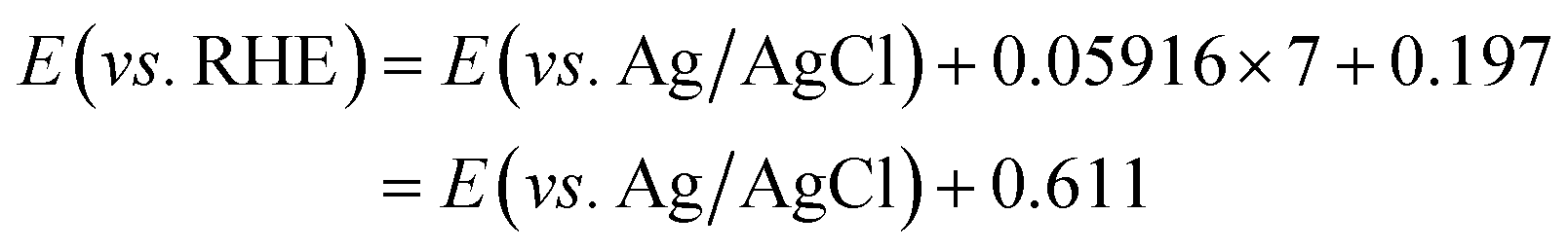
The light source used for simulated sunlight in this report was a 300-watt xenon lamp equipped with an air mass 1.5G filter (Newport). The electrochemical impedance spectroscopy (EIS) was carried out at the potential of 1.23 V vs. RHE using a potentiostat/galvanostat (PGSTAT 204, Autolab, Eco-Chemie, the Netherlands) equipped with an FRA2 module.
3. Results and discussion
In order to enhance the visible light response and charge separation efficiency of the TiO2 NR array photoanode, n/n heterojunction of a composite with stibnite Sb2S3 was synthesized. The top and side views of scanning electron microscopy (SEM) images and the transmission electron microscopy (TEM) image of TiO2 NR array are shown in Fig. 1(a) and (b), respectively. The hydrothermal TiO2 NR array presents highly ordered growth on the FTO glass, with the diameter of 50 to 300 nm and the length of around 2 μm, while the straight single TiO2 NR with the clear surface was observed in the TEM image. On the other hand, the SEM images for the unannealed and annealed TiO2/Sb2S3 nanocomposite were shown in Fig. 1(c) and (e), respectively, and the images with the high magnitude were respectively presented in Fig. 1(d) and (f). The unannealed sample shows lots of Sb2S3 aggregates growing between and on the top of the TiO2 NRs. It can be clearly found that most parts of the gaps between the NRs were filled with the Sb2S3 nanoaggregates. In the higher magnitude image, the Sb2S3 nanoparticles with the size of around 100 nm were found to cover on the top of TiO2 NRs, while some of the large chunks of Sb2S3 were observed between the TiO2 NRs. After the sample was treated by 300 °C annealing under the nitrogen atmosphere, the annealed sample with much larger Sb2S3 octahedral structures having the size of around 500 nm to 1 mm were observed between the TiO2 NRs, while some of the small Sb2S3 nanoaggregates still remained in some of the region. It is inferred that by applying the CBD method to coat Sb2S3 on the TiO2 NR array, the Sb2S3 nanoparticles can almost clad the entire TiO2 NRs. During the 300 °C heat treatment process, some of the coated Sb2S3 nanoparticle seems like undergoing a melt, re-aggregate, and recrystallized process, to form a new morphology of octahedral nanostructures. However, not all of the Sb2S3 nanoparticles transform to the octahedron structure, some of the materials still remained their original forms and covered on the TiO2 NR in irregular shapes. The XRD patterns of the TiO2 NR array, annealed TiO2/Sb2S3, and unannealed TiO2/Sb2S3 nanocomposites are shown in Fig. 2(a), which present pure rutile TiO2 peaks of (101), (211), and (002) for all of the patterns, indicating the successful synthesis of TiO2 NR by using the simple hydrothermal method. On the other hand, the Sb2S3 peaks (JCPDS 42-1393)24 are only observed in the annealed TiO2/Sb2S3 sample, while the unannealed TiO2/Sb2S3 sample presents only the peaks for TiO2. To investigate this phenomenon, the XRD patterns for the annealed Sb2S3 and the unannealed Sb2S3 samples were further measured as shown in the same figure. The Sb2S3 peaks are only observed for the annealed sample, and the unannealed one presents no peaks corresponding to Sb2S3, indicating its amorphous nature. Hence, it is reasonable that the unannealed TiO2/Sb2S3 sample presents no peaks corresponding to Sb2S3. Only with the annealing treatment the Sb2S3 presents crystalline feature which can be observed in both annealed TiO2/Sb2S3 and annealed Sb2S3 samples. To further confirm the existing of Sb2S3 in the composite, energy-dispersive X-ray spectroscopy (EDX) was applied to analyze the elements for the annealed and unannealed composites as shown in Fig. 2(b) and (c), respectively. The signals for Sb, S, Ti and O are clearly observed for both of the samples, while the atomic ratio of Sb and S indicates the formation of Sb2S3 for the annealed sample but the unannealed one presents a form closed to Sb5S4. The EDX results illustrate that the amount of Sb2S3 is far less than that of TiO2.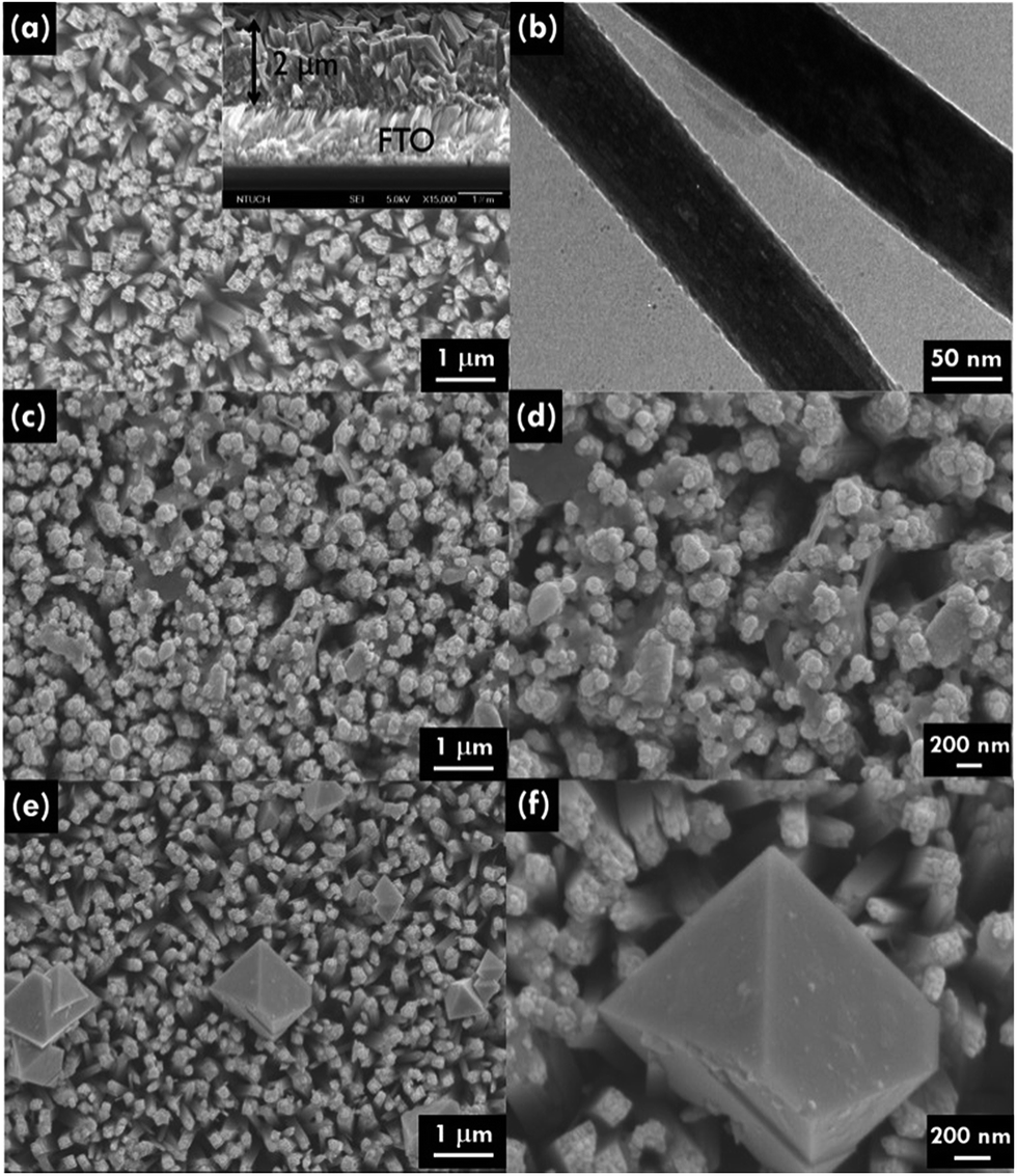 | ||
| Fig. 1 (a) The top and side-view of the SEM image for the TiO2 NRs array, (b) the TEM image of two single TiO2 NRs, and the SEM images for (c and d) the unannealed and (e and f) annealed TiO2/Sb2S3 nanocomposites. | ||
 | ||
| Fig. 2 (a) The XRD patterns for the TiO2 NR array, unannealed TiO2/Sb2S3 and annealed TiO2/Sb2S3 nanocomposites, as well as unannealed Sb2S3 and annealed Sb2S3 powders, and the EDX spectra for (b) the unannealed TiO2/Sb2S3 and (c) the annealed TiO2/Sb2S3 nanocomposites. | ||
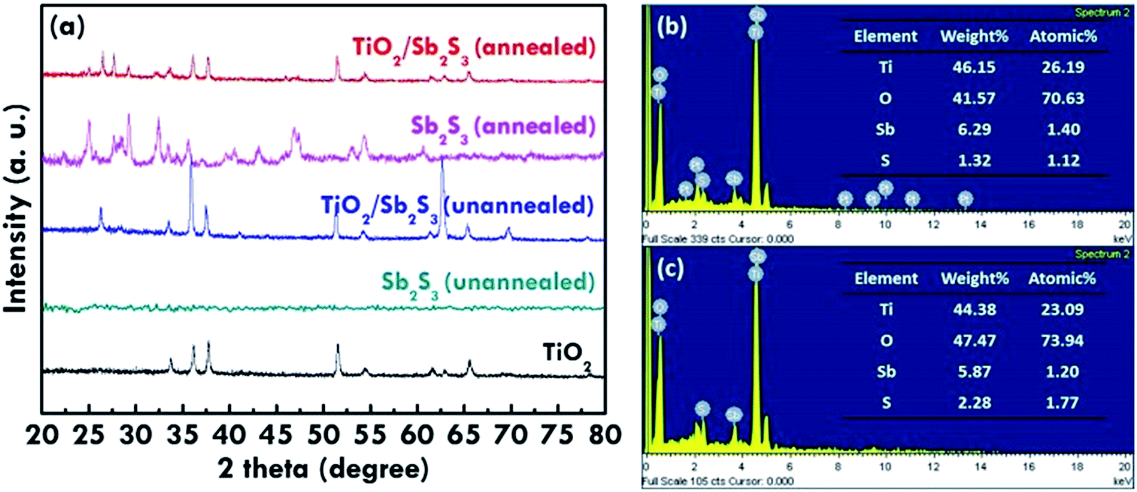
Moreover, the morphology distribution of the TiO2/Sb2S3 nanocomposite to the corresponding compound was examined by the EDX elemental mapping. The spatial elemental distributions of Ti, O, Sb, and S and the corresponding SEM image were shown in Fig. 3. It is clearly to find that the main Sb and S signals distribute completely on the octahedron structure region, and the main Ti and O signals can only be observed out of this portion, indicating the octahedron morphology is truly Sb2S3. The previous literature also applied the chemical bath deposition method to synthesize Sb2S3, and the octahedron structure was also obtained.25 In addition, the color of white, yellow, and black were respectively observed for the TiO2 NR array, unannealed TiO2/Sb2S3, and annealed TiO2/Sb2S3 nanocomposites, as shown in Fig. S1 in the ESI.† The obvious color change again suggests the successful combination of these two materials and also confirms the different phases for the nanocomposites with and without annealing.
 | ||
| Fig. 3 The EDX mapping spectra for the signals obtained from Ti Kα1 orbital, O Kα1 orbital, S Kα1 orbital, and Sb Lα1 orbital of the annealed TiO2/Sb2S3 nanocomposite. The corresponding SEM image was also presented in this figure. | ||
The absorption features for the TiO2 NR array, annealed TiO2/Sb2S3, and unannealed TiO2/Sb2S3 nanocomposites measured by the UV-visible spectroscopy are shown in Fig. 4(a). The pure TiO2 NR array only absorbs light below 400 nm, but the light absorption extends to visible region (∼550 nm) with Sb2S3 coating due to its narrow band gap,14,15 and even extend to 750 nm after treating the sample with 300 °C annealing. The result is consistent with the color change of the corresponding films. The optical band gap was determined by the Tauc plot with a linear extrapolation26 in Fig. 4(b) by the following Tauc equation,27
| (αhν)n = A(hν − Eg) |
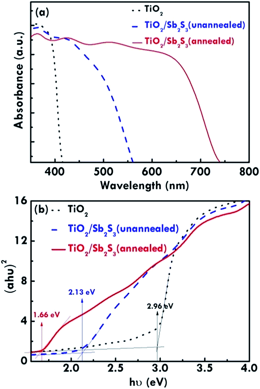 | ||
| Fig. 4 (a) Absorption spectra and (b) Tauc plots for the TiO2 NR array, unannealed TiO2/Sb2S3, and annealed TiO2/Sb2S3 nanocomposites photoanodes. | ||
Having confirmed the absorption enhancements for the photoanodes with Sb2S3 coating, the photoelectrochemical properties of the TiO2 NR array, the unannealed TiO2/Sb2S3 and the annealed TiO2/Sb2S3 photoanodes were studied by evaluating the corresponding current density–voltage (J–V) curves under simulated AM 1.5G illumination at the power density of 100 mW cm−2 as shown in Fig. 5(a), and the dark current measured without the illumination was also presented for comparison. The dark currents for all the samples are very similar and the current values are close to zero at all the voltage, so only one of the dark currents was shown in this figure. The onset potential of 0.16, 0.01, and −0.08 V vs. RHE were found for the photoanodes with the TiO2 NR array, the unannealed TiO2/Sb2S3, and the annealed TiO2/Sb2S3 nanocomposites. The negative shift on the onset potential for the Sb2S3 coated TiO2 NRs array as compared with that for the pure TiO2 electrode is due to the more negative CB potential of the coated Sb2S3. This result is also observed in the previous literature.33 This phenomenon is advantageous for the Z-scheme system which requires low onset potential for photoanodes to integrate with a photocathode.34 A saturated photocurrent density of 0.79 mA cm−2 (measured at 1.23 V vs. RHE) was obtained for the photoanode with the annealed TiO2/Sb2S3 nanocomposite, which is eight-fold higher than those of the photoanodes with the unannealed TiO2/Sb2S3 nanocomposite (0.10 mA cm−2) and the TiO2 NR array (0.09 mA cm−2) measured at the same condition. The photocurrent is generated by firstly separating the electron/hole pairs in the nanomaterial by the incident light, the charges were then transported through the material, and finally the charges were transferred to the substrate and the electrolyte at the same time to respectively produce the photocurrent and do the photoelectrochemical water splitting reactions. The great enhancement on the photocurrent density for electrode with the annealed TiO2/Sb2S3 nanocomposite is mainly due to the broader and higher light absorption by the annealed Sb2S3 light absorber to separate more electron/hole pairs in the first step of the photocurrent generation. Also, the annealed and the unannealed Sb2S3 are in the crystallized and the amorphous features, respectively. The crystallized Sb2S3 is inferred to have higher charge transport rate, leading to the higher photocurrent density as compared with that for the electrode with the unannealed Sb2S3. To further clarify the contribution of the incident light to the photocurrent density, the J–V curves for the annealed TiO2/Sb2S3 photoanodes measured with a UV cutoff filter were also shown in Fig. 5(a). The annealed TiO2/Sb2S3 photoanode shows smaller photocurrent density (0.49 mA cm−2 measured at 1.23 V vs. RHE) than that for the annealed TiO2/Sb2S3 photoanode measured without using a UV cutoff filter (0.79 mA cm−2 measured at 1.23 V vs. RHE). It is clearly found that without the illumination of the light in the UV region the annealed TiO2/Sb2S3 photoanode still have the photocurrent density of 0.49 mA cm−2 (measured at 1.23 V vs. RHE), indicating the coating of Sb2S3 on TiO2 can enhance the photocurrent density by absorbing and converting more incident light in the visible region to the electricity. The reduced photocurrent density of around 0.3 mA cm−2 for the TiO2/Sb2S3 photoanode measured with and without the UV cutoff filter is not only due to the loss from the current density contribution of TiO2 but also from that of the Sb2S3 layer, so the reduced photocurrent density is higher than the photocurrent density for the pure TiO2 photoanode (0.09 mA cm−2 measured at 1.23 V vs. RHE) as expected. Moreover, the Nyquist plots of TiO2, unannealed TiO2/Sb2S3, and annealed TiO2/Sb2S3 photoanodes were obtained to evaluate the charge-transfer resistance at the TiO2/Sb2S3/electrolyte interface (Rct), as shown in Fig. 5(b), and the enlarged plots at the high frequency region as well as the equivalent circuit were inserted in this figure. The Rct values were estimated by fitting the plots by using the equivalent circuit. The value of 22![[thin space (1/6-em)]](https://www.rsc.org/images/entities/char_2009.gif) 582, 7484, and 3285 Ω were respectively obtained for the TiO2, unannealed TiO2/Sb2S3, and annealed TiO2/Sb2S3 photoanodes. It is obviously observed that the semicircles as well as the Rct values obtained at the higher frequency region are smaller for the TiO2/Sb2S3 photoanodes as compared with that for the TiO2 NR array photoanode, indicating the coating of Sb2S3 can enhance the charge separation/transportation, in turn reduce the interfacial resistance. Among the TiO2/Sb2S3 photoanodes, the annealed one shows smaller semicircle as well as the smaller Rct values at the higher frequency region, revealing the post heat-treatment can help the growth of octahedral Sb2S3 nanostructure which may have better ability to improve the charge separation/transportation. In addition, the serious resistance for the system (Rs) can be evaluated by using the intercept at the x-axis. From the enlarged Nyquist plots at the higher frequency region, it is obvious that the Rs value is the smallest for the annealed TiO2/Sb2S3 photoanode, while the TiO2 photoanode presents the largest Rs value. The results again suggest the excellent performance for the TiO2 photoanode coated with the annealed light absorber Sb2S3 for enhancing the light utilization and the charge-transfer capability. To confirm the solar-driven water splitting, Fig. 5(c) shows the system's transient current response under chopped illumination (measured at 1.23 V vs. RHE) for the TiO2 NR array and the annealed TiO2/Sb2S3 photoanodes. The rapid photocurrent response to the illuminated light for both cases indicates the ability of the photocatalyst to catalyze the solar-driven photoelectrochemical water splitting reactions. Also, the long-term stability of the TiO2 NR array and the annealed TiO2/Sb2S3 photoanodes for photoelectrochemical water splitting reactions was evaluated with the photoanode held at 1.23 V vs. RHE under simulated AM 1.5G illumination using a potentiostat to monitor the photocurrent density, as shown in Fig. 5(d). The photocurrent density of TiO2 NR array photoanode remained approximately 0.10 mA cm−2 over 1200 min without degradation, but the TiO2/Sb2S3 photoanode presented a small degradation with the initial and terminal photocurrent density values of 0.79 and 0.11 mA cm−2, respectively, suggesting the that Sb2S3 is not quite stable in water and therefore improvement on the stability for the TiO2/Sb2S3 system is necessary. To further improve the stability of the TiO2/Sb2S3 photoanode in the aqueous solution, another electrolyte was prepared by mixing 0.5 M Na2SO4 and 0.5 M Na2S solutions in the equal volume. The long-term stability of the annealed TiO2/Sb2S3 photoanode for the photoelectrochemical water splitting in the electrolyte containing S2− ions contributed from Na2S was tested under the same conditions as those for measuring the long-term stability of the electrode in the electrolyte containing only Na2SO4. However, the Sb2S3 layer was found to be removed from the TiO2 layer when the electrode was soaked in the electrolyte, as shown in Fig. S2 in the ESI.† It was reported that when Na2S was dissolved in the water, the S2− ion would be released and combine with the H+ ion to form the HS− ion in the solution, and at the same time the OH− ions would be released from water, leading to the formation of the basic solution. The Sb2S3 would be dissolved in the basic solution due to its chemical property. Hence, the long-term stability of the annealed TiO2/Sb2S3 photoanode
for water oxidation cannot be tested in the electrolyte containing S2− ions as suggested by this reviewer. To enhance the stability of the TiO2/Sb2S3 photoanode in the aqueous solution, different methods like electrodeposition will be applied to improve the attachment of Sb2S3 on the TiO2 layer in our future work.
582, 7484, and 3285 Ω were respectively obtained for the TiO2, unannealed TiO2/Sb2S3, and annealed TiO2/Sb2S3 photoanodes. It is obviously observed that the semicircles as well as the Rct values obtained at the higher frequency region are smaller for the TiO2/Sb2S3 photoanodes as compared with that for the TiO2 NR array photoanode, indicating the coating of Sb2S3 can enhance the charge separation/transportation, in turn reduce the interfacial resistance. Among the TiO2/Sb2S3 photoanodes, the annealed one shows smaller semicircle as well as the smaller Rct values at the higher frequency region, revealing the post heat-treatment can help the growth of octahedral Sb2S3 nanostructure which may have better ability to improve the charge separation/transportation. In addition, the serious resistance for the system (Rs) can be evaluated by using the intercept at the x-axis. From the enlarged Nyquist plots at the higher frequency region, it is obvious that the Rs value is the smallest for the annealed TiO2/Sb2S3 photoanode, while the TiO2 photoanode presents the largest Rs value. The results again suggest the excellent performance for the TiO2 photoanode coated with the annealed light absorber Sb2S3 for enhancing the light utilization and the charge-transfer capability. To confirm the solar-driven water splitting, Fig. 5(c) shows the system's transient current response under chopped illumination (measured at 1.23 V vs. RHE) for the TiO2 NR array and the annealed TiO2/Sb2S3 photoanodes. The rapid photocurrent response to the illuminated light for both cases indicates the ability of the photocatalyst to catalyze the solar-driven photoelectrochemical water splitting reactions. Also, the long-term stability of the TiO2 NR array and the annealed TiO2/Sb2S3 photoanodes for photoelectrochemical water splitting reactions was evaluated with the photoanode held at 1.23 V vs. RHE under simulated AM 1.5G illumination using a potentiostat to monitor the photocurrent density, as shown in Fig. 5(d). The photocurrent density of TiO2 NR array photoanode remained approximately 0.10 mA cm−2 over 1200 min without degradation, but the TiO2/Sb2S3 photoanode presented a small degradation with the initial and terminal photocurrent density values of 0.79 and 0.11 mA cm−2, respectively, suggesting the that Sb2S3 is not quite stable in water and therefore improvement on the stability for the TiO2/Sb2S3 system is necessary. To further improve the stability of the TiO2/Sb2S3 photoanode in the aqueous solution, another electrolyte was prepared by mixing 0.5 M Na2SO4 and 0.5 M Na2S solutions in the equal volume. The long-term stability of the annealed TiO2/Sb2S3 photoanode for the photoelectrochemical water splitting in the electrolyte containing S2− ions contributed from Na2S was tested under the same conditions as those for measuring the long-term stability of the electrode in the electrolyte containing only Na2SO4. However, the Sb2S3 layer was found to be removed from the TiO2 layer when the electrode was soaked in the electrolyte, as shown in Fig. S2 in the ESI.† It was reported that when Na2S was dissolved in the water, the S2− ion would be released and combine with the H+ ion to form the HS− ion in the solution, and at the same time the OH− ions would be released from water, leading to the formation of the basic solution. The Sb2S3 would be dissolved in the basic solution due to its chemical property. Hence, the long-term stability of the annealed TiO2/Sb2S3 photoanode
for water oxidation cannot be tested in the electrolyte containing S2− ions as suggested by this reviewer. To enhance the stability of the TiO2/Sb2S3 photoanode in the aqueous solution, different methods like electrodeposition will be applied to improve the attachment of Sb2S3 on the TiO2 layer in our future work.
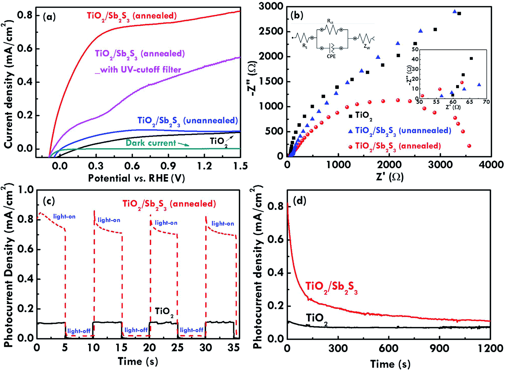 | ||
| Fig. 5 (a) The J–V plots and (b) the Nyquist plots with the enlarged plots at the high frequency region and the equivalent circuit inserted for the TiO2 NR array, unannealed TiO2/Sb2S3, and annealed TiO2/Sb2S3 nanocomposites photoanodes, (c) the transient photoresponse shown by light chopping current densities (light on/light off) as a function of time and (d) the current measurement for the stability test for the TiO2 NR array and annealed TiO2/Sb2S3 nanocomposites photoanodes. | ||
To illustrate the charge transfer of the TiO2/Sb2S3 photoanode, the band diagram of TiO2 and stibnite Sb2S3 and the electron/hole cascade were presented in Fig. 6. The conduction band (CB) edge is more negative for stibnite Sb2S3 than that for rutile TiO2.19 Therefore, along the band bending direction the photogenerated electrons in stibnite Sb2S3 will inject from the CB of stibnite Sb2S3 into the CB of rutile TiO2, and then go to the outer circuit. In the same way, since the valence band (VB) edge of rutile TiO2 is more positive than that of stibnite Sb2S3, and the VB edge of stibnite Sb2S3 is more positive than the potential for the photoelectrochemical water splitting reactions,19 the photogenerated holes in stibnite Sb2S3 are expected to transport to the electrolyte to oxidize water. Hence, the combination of Sb2S3 with TiO2 cannot only broaden the light absorption, but also improve the electron/hole transfer in the nanocomposite benefited from the relative band positions.
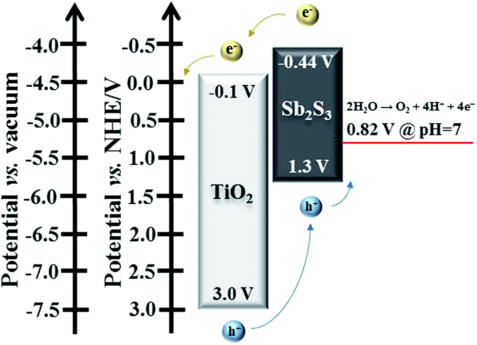 | ||
| Fig. 6 The schematic representation of band energies and charge transfer for annealed TiO2/Sb2S3 nanocomposite under illumination. | ||
Last, the comparison between the related literatures using a more commonly used TiO2/CdS system and the results obtained in this work was made regarding to the optical and electrochemical properties.35,36 Pathak et al. fabricated a three-dimensional branched TiO2 photoanode with the deposition of CdS by using the successive ionic layer adsorption and reaction (SILAR) method for the application on the photoelectrochemical water splitting reactions. The onset absorbance is extended to 536 nm for the TiO2/CdS photoanode, while the bare TiO2 photoanode only shows the onset absorbance of around 400 nm. The maximum photocurrent density for the TiO2/CdS photoanode after 15 SILAR cycles for the CdS deposition of 1.2 mA cm−2 was noted, which is higher than that of around 0.4 mA cm−2 for the bare TiO2 photoanode. The time-dependent stability analysis for the TiO2/CdS photoanode was also made with 51% decreases on the photocurrent density as compared with the initial value for 10000 s test.35 Mukherjee et al. deposited CdS on ZnO nanorods using a deposition bath containing cadmium nitrate and thioacetamide to fabricate a heterostructured optoelectronic material for the application on the methylene blue (MB) degradation. The optical absorbance was extended to 500 nm for the ZnO/CdS electrode, while the bare ZnO electrode only showed the absorbance shoulder at around 400 nm. The photocurrent density reached a saturation value of 1.5 mA cm−2 for the ZnO/CdS electrode. Also, the ZnO/CdS electrode presented 77.4% methylene blue (MB) degradation and the bare ZnO electrode showed only 37% MB degradation in the same testing conditions. However, the long-term stability test for the ZnO/CdS electrode did not present in this literature.36 Those comparisons suggested that by incorporating a visible light absorber in the electrode, i.e., Sb2S3 or CdS, the optical and the electrochemical performances can be largely enhanced as compared to those for the electrode without a visible light absorber.
4. Conclusions
In summary, the n/n heterojunction of TiO2 nanorods and Sb2S3 octahedral nanostructure was successfully developed as a photocatalyst for the photoelectrochemical water splitting reactions, with an impressive photocurrent density of 0.78 mA cm−2 and a low onset potential of −0.08 V vs. RHE as compared to those for a pure TiO2 system (0.09 mA cm−2 and 0.16 V vs. RHE respectively for the photocurrent density and the onset potential). The material and CB/VB cascade designs provide a pathway for better visible response and improved electron/hole transportation, as it explores new semiconductor material combinations with TiO2 NRs for the realization of promising materials for the photoelectrochemical water splitting reactions.Acknowledgements
This work was supported in part by the Ministry of Science and Technology of Taiwan, under grant numbers: MOST 103-2218-E-027-010-MY2 and MOST 103-2119-M-027-001-.References
- A. Fujishima and K. Honda, Nature, 1972, 238, 37–38 CrossRef CAS PubMed
.
- G. Ma, H. Peng, J. Mu, H. Huang, X. Zhou and Z. Lei, J. Power Sources, 2013, 229, 72–78 CrossRef CAS
- S. So, K. Lee and P. Schmuki, Chem.–Eur. J., 2013, 19, 2966–2970 CrossRef CAS PubMed
- R. S. Ray, B. Sarma, A. L. Jurovitzki and M. Misra, Chem. Eng. J., 2015, 260, 671–683 CrossRef CAS
- D. Yu, X. Zhu, Z. Xu, X. Zhong, Q. Gui, Y. Song, S. Zhang, X. Chen and D. Li, ACS Appl. Mater. Interfaces, 2014, 6, 8001–8005 CAS
- V. Suryanarayanan, K. M. Lee, W. H. Ho, H. C. Chen and K. C. Ho, Sol. Energ. Mat. Sol. Cells, 2007, 91, 1467–1471 CrossRef CAS
- W. Smith, A. Wolcott, R. C. Fitzmorris, J. Z. Zhang and Y. Zhao, J. Mater. Chem., 2011, 21, 10792–10800 RSC
- Y. Liu, J. Zhang, S. Wang, K. Wang, Z. Chen and Q. Xu, New J. Chem., 2014, 38, 4045 RSC
- B. Naik, S. Martha and K. M. Parida, Int. J. Hydrogen Energy, 2011, 36, 2794–2802 CrossRef CAS
- J. Kim, S. Byun, A. J. Smith, J. Yu and J. Huang, J. Phys. Chem. Lett., 2013, 4, 1227–1232 CrossRef CAS PubMed
- A. Ramadoss and S. J. Kim, Carbon, 2013, 63, 434–445 CrossRef CAS
- B. Minnaert and P. Veelaert, Energies, 2014, 7, 1500–1516 CrossRef
- D. Ke, H. Liu, T. Peng, X. Liu and K. Dai, Mater. Lett., 2008, 62, 447–450 CrossRef CAS
- N. S. Yesugade, C. D. Lokhande and C. H. Bhosale, Thin Solid Films, 1995, 263, 145–149 CrossRef CAS
- M. Y. Versavel and J. A. Haber, Thin Solid Films, 2007, 515, 7171–7176 CrossRef CAS
- K. C. Gödel, Y. C. Choi, B. Roose, A. Sadhanala, H. J. Snaith, S. I. Seok, U. Steiner and S. K. Pathak, Chem. Commun., 2015, 51, 8640–8643 RSC
- S. Ito, K. Tsujimoto, D.-C. Nguyen, K. Manabe and H. Nishino, Int. J. Hydrogen Energy, 2013, 38, 16749–16754 CrossRef CAS
- A. Darga, D. Mencaraglia, C. Longeaud, T. J. Savenije, B. O'Regan, S. Bourdais, T. Muto, B. Delatouche and G. Dennler, J. Phys. Chem. C, 2013, 117, 20525–20530 CAS
- J. Kim, Y. Sohn and M. Kang, Int. J. Hydrogen Energy, 2013, 38, 2136–2143 CrossRef CAS
- H. Xie, W. Que, Z. He, P. Zhong, Y. Liao and G. Wang, J. Alloys Compd., 2013, 550, 314–319 CrossRef CAS
- M. Sun, G. Chen, Y. Zhang, Q. Wei, Z. Ma and B. Du, J. Am. Chem. Soc., 2012, 51, 2897–2903 CAS
- J. Zhong, X. Zhang, Y. Zheng, M. Zheng, M. Wen, S. Wu, J. Gao, X. Gao, J. M. Liu and H. Zhao, ACS Appl. Mater. Interfaces, 2013, 5, 8345–8350 CAS
- J. H. Heo, S. H. Im, H. j. Kim, P. P. Boix, S. J. Lee, S. I. Seok, I. Mora Seró and J. Bisquert, J. Phys. Chem. C, 2012, 116, 20717–20721 CAS
- E. Dutková, L. Takacs, M. J. Sayagués, P. Baláž, J. Kováč and A. Šatka, Chem. Eng. Sci., 2013, 85, 25–29 CrossRef
- B. Krishnan, A. Arato, E. Cardenas, T. K. D. Roy and G. A. Castillo, Appl. Surf. Sci., 2008, 254, 3200–3206 CrossRef CAS
- J. Zhang, Z. Zhu and X. Feng, Chem.–Eur. J., 2014, 20, 10632–10635 CrossRef CAS PubMed
- B. V. Bergeron, A. Marton, G. Oskam and G. J. Meyer, J. Phys. Chem. B, 2005, 109, 937–943 CrossRef CAS PubMed
- N. Tigau, V. Ciupina, G. Prodan, G. I. Rusu, C. Gheorghies and E. Vasile, J. Optoelectron. Adv. Mater., 2004, 6, 211–217 CAS
- F. I. Ezema, A. B. C. Ekwealor, P. U. Asogwa, P. E. Ugwuoke, C. Chigbo and R. U. Osuji, Turk. J. Phys., 2007, 31, 205–210 CAS
- A. Alemi, Y. Hanifehpour and S. W. Joo, J. Nanomater., 2011, 2011, 1–6 Search PubMed
- A. Sinaoui, I. Trabelsi, F. C. Akkar, F. Aousgi and M. Kanzari, Int. J. Thin Films Sci. Technol., 2014, 3, 19–25 CrossRef
- F. I. Ezema, S. C. Ezugwu, P. U. Asogwa and A. B. C. Ekwealor, J. Ovonic Res., 2009, 5, 145–156 CAS
- H. Jung, S. Y. Chae, C. Shin, B. K. Min, O. S. Joo and Y. J. Hwang, ACS Appl. Mater. Interfaces, 2015, 7, 5788–5796 CAS
- J. F. Randall, Designing Indoor Solar Products: Photovoltaic Technologies for AES, John Wiley & Sons Ltd.: Chichester, UK, 2005 Search PubMed
- P. Pathak, S. Gupta, K. Grosulak, H. Imahori and V. Subramanian, J. Phys. Chem. C, 2015, 119, 7543–7553 CAS
- B. Mukherjee, S. Gupta, A. Peterson, H. Imahori, A. Manivannan and V. R. Subramanian, Chem.–Eur. J., 2014, 20, 10456–10465 CrossRef CAS PubMed
Footnotes |
| † Electronic supplementary information (ESI) available. See DOI: 10.1039/c6ra04094b |
| ‡ The authors contributed equally. |
| This journal is © The Royal Society of Chemistry 2016 |