
Spin-dependent Seebeck effect in zigzag black phosphorene nanoribbons
Yu-Rong Yang,
Zhao-Qian Zhang,
Lei Gu and
Hua-Hua Fu*
School of Physics and Wuhan National High Magnetic Field Center, Huazhong University of Science and Technology, Wuhan 430074, People's Republic of China. E-mail: hhfu@hust.edu.cn
First published on 29th April 2016
Abstract
As one of two-dimensional (2D) layered crystal materials, black phosphorene (BP) attracts wide interest due to its novel properties. To put BP towards device applications in spin caloritronics, here we investigate spin-dependent Seebeck effect (SDSE) in zigzag black phosphorene nanoribbons (ZBPNRs) by using first-principles calculations combined with non-equilibrium Green's function approach. The numerical results show that antiferromagnetic insulating states are stable in pristine ZBPNRs and ferromagnetic ZBPNR junctions can be constructed by an external magnetic field. By setting a different gradient between the source and the drain of the ZPNR junctions, spin-up and spin-down currents with nearly equal magnitudes are generated and flow in opposite directions, indicating that the SDSE occurs and the spin current dominates the carriers transport in the ZBPNRs. These results support that ZBPNRs are good candidates for the SDSE and have potential applications in future low-power-consumption technology.
1 Introduction
In the past decades, two-dimensional (2D) layered crystal materials with atomic thickness have attracted comprehensive attention because of their rich physical and chemical properties.1–5 As one of the outstanding representatives of 2D materials, graphene plays an important role due to its notable electronic and mechanical functionalities.6,7 Nevertheless, the absence of band gap in graphene and graphene nonoribbons largely limits their device applications in spin caloritronics, which stimulates us to search new thermoelectric materials. Recently, black phosphorene (BP), a new 2D material characterized as a mono-layer of phosphorus, has been successfully isolated from bulk- or multi-layer BP through mechanical exfoliation, since the van der Waals interaction dominates the interlay interactions in them,8 and meanwhile few-layer BP has also been fabricated by liquid-phase exfoliation.9,10 BP is the most stable allotrope of phosphorous and consists of a corrugated arrangement of P atoms and has a thickness of ∼5 Å. Alternate stacking of the later along the [001] direction gives rise to the structure of bulk BP, which is stabilized by week dispersive interactions. More importantly, BP has a considerably large band gap11–14 and an reasonably high on/off ratio of 104,15 which determine that BP is a natural p-type semiconductor with potential device applications.16–20According to the direction of termination, BP has two typical crystal ribbon orientations, i.e., armchair BP nanoribbons (ABPNRs) and zigzag BP nanoribbons (ZBPNRs), which have different electronic structures. ABPNRs are semiconductors for all edge groups while ZBPNRs have either semiconducting or metallic behavior.21 The pristine ZBPNRs have a stable magnetic state with ferromagnetic (FM) ordering in the same edge due to their dangling bonds at the zigzag edges, but have antiferromagnetic (AFM) ordering between two opposite edges in the ground states.22 Moreover, these magnetic states are stable independent of the width of ZBPNRs.23 Based on those particular magnetic properties, in this work we will explore further the occurrence of spin-dependent Seebeck effect (SDSE) in ZBPNRs. The SDSE refers to a spin current and an associated spin voltage can be produced by the temperature gradient in devices or materials.24 To realize the aim, we construct a ferromagnetic ZBPNR junction composed of the source and drain with the same ZBPNR by applying an external magnetic field. Using the first-principles calculations combined with non-equilibrium Green's function technique,25–28 we find that by adopting temperature difference between the source and the drain, spin-up and spin-down currents with nearly equal magnitudes are generated and flow in opposite directions, indicating that a good SDSE occurs in the ZBPNR junctions. Moreover, the magnitude of the thermal-induced spin current is much larger than that of the net charge current, indicating that the carrier transport in the ZBPNR junctions is dominated by the spin current.
The remainder of this paper is organized as follows. In Section 2, based on the calculations of band structures, the stable magnetic states of ZBPNRs are obtained. In Section 3, the thermally driven spin-dependent transport properties of ZBPNRs are introduced, the SDSE is investigated and the physics mechanism is analyzed and finally, a conclusion is provided.
2 Band structure and magnetic states in ZBPNRs
By using Cambridge Sequential Total Energy Package (CASTAP) calculation of Materials Studio (MS), the relaxed lattice constants for monolayer BP are a = 3.295 Å, b = 4.618 Å, which are consistent with other theoretical calculations.29–31 To abide by the convention about the graphene nanoribbons,10,11 we need determine the electronic and magnetic properties of pristine N-ZBPNR, where N denotes the number of saw-like lines across the ribbon width as shown in Fig. 1(a). Firstly, the band structures of AFM and FM ordering in the 4-ZBPNR are calculated and shown in Fig. 1(b) and (c). For the 4-ZBPNR with AFM ordering, there is a large band gap, while the band structure for the 4-ZBPNR with FM ordering, the π and π* bands, which are located in the p orbitals and responsible for the low-energy electronic properties of BP, are splitting largely. Considering the device applications in spin caloritronics, we focus on the ZBPNRs with FM ordering. As N increases, the spin-up and spin-down bands are separated from each other, which is consistent with the previous report.22 Moreover, as N increases to a large value, for example N = 15, there appears a spin-splitting band gap around the Fermi level, and the spin-down bands are located above the Fermi level while the spin-up ones are below the Fermi level symmetrically, as shown in Fig. 1(g). This spin splitting band structures support that above the Fermi level, the nanoribbon provides a tunnelling path for the spin-down electrons, and below the Fermi level, the nanoribbon provides a path for the spin-up electrons, supporting that the ZBPNRs with FM ordering possess particular device applications.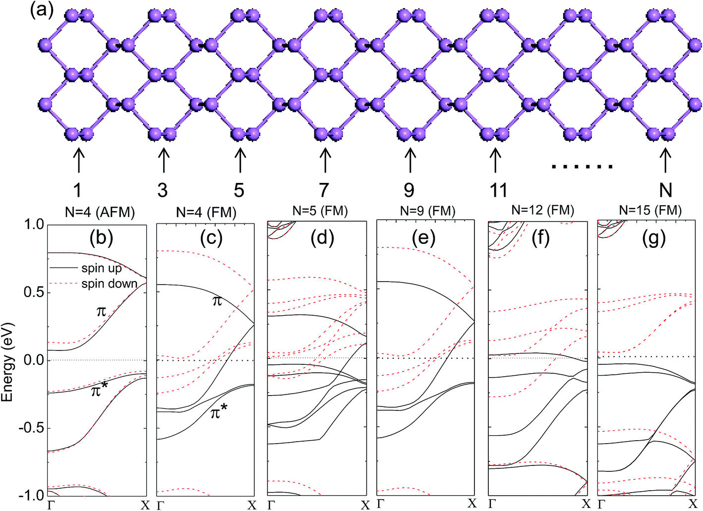 | ||
| Fig. 1 (a) Top view of ball-and-stick model of ZBPNRs. (b) and (c) The band structures of the 4-ZBPNR with antiferromagnetic ordering and ferromagnetic ordering, respectively. (d)–(g) Band structures of the ferromagnetic ZBPNRs with different ribbon widths. | ||
3 The spin-dependent Seebeck effect in ZPNRs
To explore the SDSE in ZBPNRs, we construct a spin caloritronics device, in which the source and the drain are constructed by the same ZBPNR with FM ordering, as shown in Fig. 2(a). The temperatures in the source and drain are set as TL and TR respectively, thus the temperature difference between them is ΔT = TL − TR. To grasp the spin-dependent transport characteristics, we take the device composed of the 15-ZBPNR as an example, and the results can be extended to other ZBPNR junctions with different width. The details to calculate the thermal spin-dependent currents, one can refer to our previous papers.32,33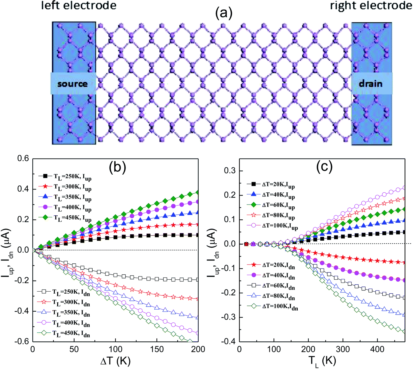 | ||
| Fig. 2 (a) The schematic illustration of the ZBPNR junction, where the source, the drain and the central scattering are adopted by the same ZBPNR with ferromagnetic ordering. (b) The spin-up current Iup and the spin-down current Idn versus TL for different values of ΔT. (c) Iup and Idn versus ΔT for different values of the source temperature TL. | ||
In Fig. 2(b), the spin-up current Iup and spin-down current Idn versus the device temperature TL under various temperature gradient ΔT are plotted. Obviously, the spin-dependent currents are generated in the device, and Iup is negative while Idn is positive, indicating that Iup flows from the drain to the source, while Idn flows from the source to the drain. Since the spin-up and spin-down currents just flow in opposite directions, we believe that the SDSE occurs in the current ZBPNR. Moreover, for all values of ΔT, the magnitude of Iup nearly equals to that of Idn, indicating that a well-defined SDSE appears here. To confirm this conclusion, the spin-dependent currents versus the temperature difference ΔT are also calculated and plotted in Fig. 2(c). One can see that as ΔT increases, for all values of TL, the flowing directions of Iup and Idn keep opposite, indicating the SDSE maintains in a large temperature region, which supports that the SDSE is stable in the device.
To understand the physical mechanism of the SDSE, we turn to analyze the band structures and the transmission spectra of the 15-ZBPNR with FM ordering. In Fig. 3(a)–(c), we presented the band structures of the source and the drain, and the transmission spectrum of the junction. One can see that the bonding π band and anti-bonding π* band appear near the Fermi level. Since the source and the drain are constructed by the same material, there is no any difference in the band structures as shown in Fig. 3(a) and (c). Moreover, as shown in the central panel of Fig. 3(b), near the Fermi level, the spin-dependent transmission spectra of the junction has a conductance peak in the energy range −0.2 eV < E < −0.04 eV and 0.04 eV < E < 0.45 eV for the spin-up and spin-down electrons, respectively. The transmission peak for the spin-down electrons locates above the Fermi level, and thus, carriers (electrons) can transport from the drain to the source, resulting in a negative spin-down current, as shown in Fig. 2(b) and (c). On the other side, the transmission peak for the spin-up electrons is below the Fermi level, and the carriers (holes) transport leads to a positive spin-up current from the source to the drain. As a result, the SDSE appears in the ZBPNR junction.
 | ||
| Fig. 3 (a) and (c) The band structures of the left panel and the right panel of the 15-ZBPNR junction; (b) the spin-dependent transmission spectra of the junction. | ||
Nevertheless, the SDSE is not perfect here, since the magnitude of Iup is not equal to that of Idn, indicating that there remains a net charge current flowing through the ZBPNR junction. This is due to the fact that the transmission peaks for the spin-up and the spin-down electrons are not well symmetrical to the Fermi level. From the spin-dependent transmission spectra plotted in Fig. 3(b), one can find that for the spin-up transmission, although the conductance channel in the region [−0.2 eV, −0.04 eV] is open, the internal of the peak is changing constantly. For example, in the energy regions [−0.1 eV, −0.04 eV] and [−0.13 eV, −0.1 eV], as the energy decreases, the conductance peak increases firstly then decreases, while in the region [−0.2 eV, −0.14 eV], the peak decreases linearly. However, for the spin-down transmission, the conductance plateau keeps stable in the region [0.04 eV, 0.35 eV] while in the region [0.35 eV, 0.47 eV], the transmission oscillates intensively. As a result, Iup and Idn distribute asymmetrically on both sides of the Fermi level.
Based on the above characteristics of the spin-dependent transport, we can obtain the thermally driven total spin current IS (=Iup − Idn) and the net charge current IC (=Iup + Idn) versus TL in Fig. 4(a) and (b), and versus ΔT in Fig. 4(c)–(d). As we expected, the magnitude of IS is much larger, even dozens of times, than that of IC, confirming the conclusion that the carrier transport through the ZBPNR junction is dominated by the spin current but not the charge current. This transport characteristic indicates the spin caloritronics device based on the ZBPNRs has potential applications in future low-power-consumption technology. It should be noted that the conclusion can be extended to other ZBPNRs with different widths, which is due to the facts that the magnetic state is stable independent of the width of ZBPNRs, and the spin-up and spin-down tunneling paths still exist above and below the Fermi level respectively, since the spin splitting band gap increases as the ribbon wide increases.23 In addition, the SDSE is possible to occur in the few-layer BP, since the FM ordering in them is easy to achieve by an external magnetic field and the spin-splitting band gap remains as the number of the layers increases.8–10 We will explore this point in our future study.
 | ||
| Fig. 4 (a) and (b) The thermally induced total spin current IS and the net electron current IC in the 15-ZBPNR junction versus TL for different values of ΔT. (c) and (d) IS and IC versus ΔT for different values of TL in the same ZBPNR junction. | ||
4 Conclusions
Through the investigations into the intrinsic magnetic states in ZBPNRs, we find that the ferromagnetic ZBPNRs can provide two independent tunneling paths for the spin-up and spin-down electrons, and they are just located above and below the Fermi level respectively. If we construct a spin caloritronic device based on the ZBPNRs with FM ordering and apply a temperature gradient between the source and the drain, the spin-dependent currents are generated and flow in opposite directions, indicating that the SDSE occurs in ZBPNRs. Although the net charge current still remains in the device, the magnitude of the total spin current is larger than that of the net charge current, indicating the carrier transport through the ZBPNR junctions is dominated by the spin current. These transport characteristics support that ZBPNRs have potential device applications in future low-power-consumption technology.Acknowledgements
We acknowledge generous financial support from “the National Natural Science Foundation of China (No. 11274128, 10804034 and 11074081)”.References
- K. S. Novoselov, A. K. Geim, S. V. Morozov, D. Jiang, Y. Zhang, S. V. Dubonos, I. V. Grigorieva and A. A. Firsov, Science, 2004, 306, 666 CrossRef CAS PubMed.
- M. I. Katsnelson, Graphene: Carbon in Two Dimensions, Cambridge University Press, Cambridge, 2012 Search PubMed.
- A. Lopez-Bezanilla, J. Huang, H. Terrones and B. G. Sumpter, Nano Lett., 2011, 11, 3267 CrossRef CAS PubMed.
- K. F. Mak, C. Lee, J. Hone, J. Shan and T. F. Heinz, Phys. Rev. Lett., 2010, 105, 136805 CrossRef PubMed.
- X. Yang and J. Ni, Phys. Rev. B: Condens. Matter Mater. Phys., 2005, 72, 195426 CrossRef.
- A. H. Castro Neto, F. Guinea, N. M. R. Peres, K. S. Novoselov and A. K. Geim, Rev. Mod. Phys., 2009, 81, 109 CrossRef CAS.
- D. S. L. Abergel, V. Apalkov, J. Berashevich, K. Ziegler and T. Chakraborty, Adv. Phys., 2010, 59, 261 CrossRef CAS.
- G. Sansone, L. Maschio, D. Usvyat, M. Schütz and A. Karttunen, J. Phys. Chem. Lett., 2016, 7, 131–136 CrossRef CAS PubMed.
- D. Hanlon, C. Backes, E. Doherty, C. S. Cucinotta, N. C. Berner, C. Boland, K. Lee, A. Harvey, P. Lynch, Z. Gholamvand, S. Zhang, K. Wang, G. Moynihan, A. Pokle, Q. M. Ramasse, N. McEvoy, W. J. Blau, J. Wang, G. Abellan, F. Hauke, A. Hirsch, S. Sanvito, D. D. O'Regan, G. S. Duesberg, V. Nicolosi and J. N. Coleman, Nat. Commun., 2015, 6, 8563 CrossRef CAS PubMed.
- P. Yasaei, B. Kumar, T. Foroozan, C. Wang, M. Asadi, D. Tuschel, J. E. Indacochea, R. F. Klie and A. Salehi-Khojin, Adv. Mater., 2015, 27, 1887–1892 CrossRef CAS PubMed.
- T. Takahashi, H. Tokailin, S. Suzuki, T. Sagawa and I. Shirotani, J. Phys. C: Solid State Phys., 1985, 18, 825–836 CrossRef CAS.
- C. Q. Han, M. Y. Yao, X. X. Bai, L. Miao, F. Zhu, D. D. Guan, S. Wang, C. L. Gao, C. Liu, D. Qian, Y. Liu and J.-F. Jia, Phys. Rev. B: Condens. Matter Mater. Phys., 2014, 90, 085101 CrossRef.
- V. Tran, R. Soklaski, Y. Liang and L. Yang, Phys. Rev. B: Condens. Matter Mater. Phys., 2014, 89, 235319 CrossRef.
- A. N. Rudenko and M. I. Katsnelson, Phys. Rev. B: Condens. Matter Mater. Phys., 2014, 89, 201408 CrossRef.
- H. Liu, A. T. Neal, Z. Zhu, D. Tomanek and P. D. Ye, ACS Nano, 2014, 8, 4033 CrossRef CAS PubMed.
- L. K. Li, Y. J. Yu, G. J. Ye, Q. Q. Ge, X. D. Ou, H. Wu, D. L. Feng, X. H. Chen and Y. B. Zhang, Nat. Nanotechnol., 2014, 9, 372 CrossRef CAS PubMed.
- S. R. Eugenie, Nature, 2014, 506, 19 CrossRef PubMed.
- W. F. Li, G. Zhang and Y. W. Zhang, J. Phys. Chem. C, 2014, 118, 22368 CAS.
- Z. Y. Ong, Y. Q. Cai, G. Zhang and Y. W. Zhang, J. Phys. Chem. C, 2014, 118, 25272 CAS.
- Y. Q. Cai, G. Zhang and Y. W. Zhang, Sci. Rep., 2014, 4, 6677 CrossRef CAS PubMed.
- X. Peng and Q. Wei, reprint arXiv, 1404–5995.
- Z. Zhu, C. Li, W. Yu, D. Chang, Q. Sun and Y. Jia, Appl. Phys. Lett., 2014, 105, 113105 CrossRef.
- Y. Du, H. Liu, B. Xu, L. Sheng, G. Yin, C.-G. Duan and X. Wan, Sci. Rep., 2015, 5, 8921 CrossRef CAS PubMed.
- K. Uchida, S. Takahashi, K. Harii, J. Ieda, W. Koshibae, K. Ando, S. Maekawa and E. Saitoh, Nature, 2008, 455, 778 CrossRef CAS PubMed.
- D. D. Wu, H. H. Fu, L. Gu, Y. Ni, F. X. Zu and K. L. Yao, Phys. Chem. Chem. Phys., 2014, 16, 17493–17498 RSC.
- H. H. Fu and K. L. Yao, Appl. Phys. Lett., 2012, 100, 013502 CrossRef.
- H. H. Fu, K. L. Yao and Z. L. Liu, J. Chem. Phys., 2008, 129, 134706 CrossRef PubMed.
- H. H. Fu, K. L. Yao and Z. L. Liu, J. Phys. Chem. A, 2008, 112, 6205–6210 CrossRef CAS PubMed.
- H. Guo, N. Lu, J. Dai, X. Wu and X. C. Zeng, J. Phys. Chem. C, 2014, 118, 14051 CAS.
- Z. Zhu, Z. G. Fthenakis, J. Guan and D. Toma’nek, Phys. Rev. Lett., 2014, 112, 026803 CrossRef PubMed.
- C. M. Jaworski, J. Yang, S. Mack, D. D. Awschalom, J. P. Heremans and R. C. Myers, Nat. Mater., 2010, 9, 898 CrossRef CAS PubMed.
- H. H. Fu, D. D. Wu, Z. Q. Zhang and L. Gu, Sci. Rep., 2015, 5, 10547 CrossRef PubMed.
- H. H. Fu, D. D. Wu, L. Gu, M. Wu and R. Wu, Phys. Rev. B: Condens. Matter Mater. Phys., 2015, 92, 045418 CrossRef.
| This journal is © The Royal Society of Chemistry 2016 |