
Large-area high quality MoS2 monolayers grown by sulfur vapor counter flow diffusion†
Bo Chen,
Qingxuan Yu*,
Qiuyun Yang,
Pengfei Bao,
Wenlong Zhang,
Liren Lou,
Wei Zhu and
Guanzhong Wang*
Hefei National Laboratory for Physical Sciences at the Microscale and Department of Physics, University of Science and Technology of China, Hefei, Anhui 230026, People's Republic of China. E-mail: yuqx@ustc.edu.cn; gzwang@ustc.edu.cn; Fax: +86-551-63606266; Tel: +86-551-63603323
First published on 12th May 2016
Abstract
Large-area uniform monolayer MoS2 films are prepared via an atmospheric pressure chemical vapor deposition method. Sulfur vapor counter flow diffusion lowers its concentration at the reaction zone and makes MoO3 sulfurization slow and gentle, which is beneficial for monolayer MoS2 growth. Suboxide MoO3−x domains, co-existing MoS2 mono- and multi-layers, monolayer MoS2 films, triangular MoS2 monolayer flakes are successively formed in the growth zone along the gas flow direction. Optical microscopy, atomic force microscopy, transmission electron microscopy, UV-vis, Raman and photoluminescence spectra demonstrate that the as-grown films are continuous monolayers over a large area, and are of high quality comparable to exfoliated monolayer MoS2. This method can also be applied to synthesize MoS2/MoO2 microplates without the assistance of metal oxides.
1. Introduction
Graphene has shown many exotic physical phenomena and remarkable properties,1–7 but its zero band gap is not suitable for application in logic electronics.8 In this regard, transition-metal dichalcogenides (TMDs) have recently emerged as the most promising alternative to graphene. As a member of the TMD family, molybdenum disulfide (MoS2) exhibits many excellent properties when thinned to the monolayer regime, such as intrinsic direct gap structure,9,10 band structure tunability with strain,11–14 valley-selective circular dichroism,15–19 highly reactive edge sites for hydrogen evolution reaction (HER),20–26 excellent on/off ratio of ∼108 and high carrier mobility up to 200 cm2 V−1 s−1 at room temperature,27 integration versatility,28,29 etc. Thus, there is a critical need to develop reliable and flexible synthesis methods for monolayer MoS2 to utilize these fantastic properties.Until now, two major strategies have been employed to obtain MoS2 atomically thin layers. Initially the top-down methods relying on exfoliation of layered bulk crystals were widely adopted, including scotch tape assisted micromechanical exfoliation,30 electrochemical Li-intercalation and exfoliation,31 liquid phase exfoliation by direct sonication in solvents,32,33 and laser or plasma thinning.34,35 These methods only allow us to produce nanometer- to micrometer-sized monolayers. Recently, several bottom-up approaches, such as thermolysis of ammonium thiomolybdate,36,37 sulfurization of molybdenum38–40 or molybdenum oxide film,41 physical vapor deposition,42 and atomic layer deposition,43,44 have been exploited to synthesize MoS2 on insulating substrates. However, none of the processes have the capability of large-area growth of uniform MoS2 monolayers. Compared with the routes mentioned above, chemical vapor deposition (CVD) has been proven a more suitable technique for synthesizing MoS2 film with control over layer number,45–47 nucleation,48–50 grain size,51 and lattice orientation52–54 due to its broad tunability in growth parameters. Despite the above progresses, current growth of monolayer MoS2 is still in a nascent stage.
Yu et al.46 demonstrated that for an exclusive growth of MoS2 monolayer in CVD process, partial pressure of gaseous MoS2, PMo, should lie between the vapor pressures of MoS2 monolayer (POMo,1) and bilayer (POMo,2) films as POMo,1 < PMo < POMo,2. So in previous works, low pressure is often employed in MoS2 monolayer synthesis since PMo is proportional to the total pressure when precursor amount is constant and Mo precursor vapor is fully reacted. The synthesized film is polycrystalline with grain size ranges from tens of nanometers to micrometers.46,51,52 While at atmospheric pressure, sulfur vapor concentration is so high that sulfurization reaction is violent and partial pressure of gaseous MoS2 is too large for monolayer MoS2 to grow (Fig. S1†). Therefore, moderating sulfurization reaction to lower the partial pressure of gaseous MoS2 may be a feasible way to synthesize monolayer MoS2 at atmospheric pressure.
Here we report the CVD synthesis of large-area uniform monolayer MoS2 film at atmospheric pressure by placing sulfur powder downstream relative to the gas flow direction instead of upstream as usually adopted in previous studies. The dependence of products on the distance away from MoO3 precursor and the flow rate of carrier gas were investigated. The quality of the as-grown film was evaluated by Raman, photoluminescence, UV-vis and transmission electron microscope measurements. Furthermore, MoS2/MoO2 microplates can also be grown using this method without the need of adding metal oxides to assist the synthesis.
2. Experimental section
2.1 CVD growth of monolayer MoS2 on sapphire
The experimental setup to synthesize monolayer MoS2 on sapphire is illustrated in Fig. 1b. A tubular furnace equipped with a quartz tube (length 100 cm, inner diameter 3.2 cm) was employed to conduct the growth. The length of the heating zone of the furnace is 18 cm. 6 mg of MoO3 powder was placed at the upstream entry of the furnace and 200 mg of sublimated sulfur was located downstream. Well cleaned sapphire (0001) substrates were put downstream in a distance of 6.5 cm away from the center of furnace (the distance between MoO3 and sapphire is 17.5 cm). The CVD growth was performed at atmospheric pressure. After flushing the tube with Ar carrier gas for two times, the furnace was heated up to 820 °C at a rate of 20 °C min−1 with 50 sccm Ar (sccm denotes standard cubic centimeter per minute), held at 820 °C for 20 min, and then naturally cooled down to room temperature. | ||
| Fig. 1 Synthesis and optical characterizations of monolayer MoS2 on sapphire. (a) Schematic view of the surface growth. (b) Experimental setup of the CVD system. (c) Photograph of a bare sapphire substrate and one nearly full covered by MoS2 film. (d and e) High and low magnification optical microscope images of monolayer MoS2 film. (f) Optical microscope image of coalescence of MoS2 domains, with lateral size of about 150 μm. (g) XPS scans for Mo and S binging energies of bulk and CVD MoS2. (h and i) Typical Raman and normalized PL spectra comparisons between our synthesized MoS2 and an exfoliated one. The PL intensity is normalized by Raman A1g phonon peak at ∼525.4 nm (400.7 cm−1 in Raman shift). Inset is the magnified spectra showing characteristic Raman peaks. (j) UV-vis absorbance spectrum of monolayer MoS2 film. | ||
2.2 Micromechanical exfoliation of monolayer MoS2 on sapphire
To obtain monolayer MoS2 from its bulk form, scotch tape assisted micromechanical exfoliation method was adopted. Firstly a MoS2 flake was mechanically exfoliated from a bulk MoS2 crystal using 3M scotch tape. Then the tape was folded, pressed gingerly and peeled slowly so that the MoS2 flake cleaved smoothly into two, this step was repeated for about six to eight times. Next, the cleaved MoS2 flake that remained stuck to the tape was laid onto a sapphire substrate and rubbed by using a plastic tweezer. After that, the tape was peeled off slowly with the plastic tweezer. Finally, the sapphire substrate was placed under an optical microscope to find the monolayer MoS2 sample (Fig. S2†).2.3 Characterization
Optical images were taken on an Olympus BX51M microscope. X-ray photoemission spectroscopy (XPS) measurements were performed on Thermo Scientific Escalab 250Xi system using an Al Kα X-ray source and energy calibrations were made against C 1s peak to eliminate the charging of sample during analysis. Raman and photoluminescence (PL) spectra were collected by JY Horiba HR800 micro-Raman spectrometer with an excitation wavelength of 514 nm. UV-vis absorbance spectrum was measured using Shimadzu SolidSpec-3700DUV spectrophotometer. Tapping-mode atomic force microscope (AFM) measurements were done on a Bruker Dimension Icon microscope. Transmission electron microscope (TEM) images and selected area electron diffraction (SAED) pattern were captured using JEOL JEM-2010F operated at 200 kV.3. Results and discussion
Fig. 1a schematically illustrates the MoS2 growth process on sapphire (0001) substrate. In brief, upstream MoO3 was partially reduced by sulfur vapor from downstream S source to form volatile suboxide MoO3−x species. These suboxide compounds were conveyed by Ar carrier gas and reacted with sulfur to give rise to the formation of MoS2 on sapphire. The stepwise reaction process of MoO3 and S can be described by the following equations:55
 | (1) |
 | (2) |
The CVD setup employed in this work is depicted in Fig. 1b. Macroscopic photograph in Fig. 1c clearly presents the color contrast between a bare substrate and an as-grown sample. Further optical microscope images (Fig. 1d and e) demonstrate that the as-prepared monolayer MoS2 film is uniform and continuous over a large area, with the constituent domains of about 150 μm in edge length (Fig. 1f).
Chemical state and composition of the products were analyzed through XPS. As seen from Fig. 1g, there are two prominent groups of peaks. One is the peaks associated with Mo4+, peaking at 230.2 eV (3d5/2) and 233.3 eV (3d3/2), and the other can be assigned to S2−, peaking at 163.1 eV (2p3/2) and 164.3 eV (2p1/2). These peaks closely match with those of the bulk MoS2 (Mo 3d5/2 and 3d3/2 states at binding energies of 230.1 and 233.2 eV and 2p3/2 and 2p1/2 states of S at binding energies of 162.9 and 164.1 eV, respectively).
Raman and PL measurements were performed to check the quality and layer number of the as-grown MoS2 film. As a comparison, exfoliated monolayer MoS2 on sapphire was also included as a control sample. Fig. 1h shows the acquired Raman spectra, from which two characteristic Raman modes can be found. The A1g mode correlates with the out-of-plane vibration of S atoms and the E12g mode relates with the in-plane vibration of Mo and S atoms. For the synthesized MoS2 film, the full width at half maximum (FWHM) of A1g and E12g are 6.4 and 2.4 cm−1, respectively. Spacing between the two modes (Δk) is ∼17.7 cm−1. All of them are close to the exfoliated monolayer MoS2 (FWHM values of A1g and E12g are 4.6 and 1.7 cm−1, respectively, with Δk ∼ 17.7 cm−1). Meanwhile, similar PL peaks can be found from both synthesized and exfoliated MoS2 monolayers, as shown in Fig. 1i, where the PL spectra were normalized by Raman A1g peak intensity to rule out the external effects.10 Two peaks located at ∼627 and ∼678 nm are originated from direct excitonic transitions between minimum of conduction band and maxima of split valence bands (B and A excitons) in MoS2.9,10 Note that the PL peak width of our CVD monolayer MoS2 (128 meV) is a little narrower than that of exfoliated MoS2 (133 meV). These results confirm the monolayer nature and high quality of our MoS2 film as compared with the exfoliated one.
Taking advantage of the optical transparency of sapphire substrate, we further conducted UV-vis absorption characterization of the as-deposited monolayer MoS2 sample (Fig. 1j). The resulting spectrum exhibited A and B excitonic absorption bands at 664 nm (1.871 eV) and 616 nm (2.017 eV), with energy difference of about 0.146 eV, which is in good agreement with the theoretical value of 0.148 eV calculated for monolayer MoS2.56 This demonstrates not only the fine electronic structure but also the high optical quality and uniformity of our obtained monolayer MoS2 film.
Although A and B direct excitonic transitions can be readily identified from the UV-vis absorbance spectrum in Fig. 1j, PL spectra in Fig. 1i show obvious the A exciton peak, while the peak relates to B exciton is rather limited. However, in ref. 10, B exciton peak can be clearly observed in exfoliated MoS2 monolayer, bilayer, and hexalayer samples on SiO2/Si substrate. We attribute this phenomenon to different substrate-induced electron doping effects. Mak et al.57 showed that the A exciton peak intensity is highly dependent on doping, the higher the electron doping density, the lower the A exciton peak intensity; while the B exciton peak intensity has little dependence on doping. For freestanding MoS2 monolayers without electron doping from the substrate, the A exciton peak intensity is so high that the B exciton peak can not be observed.9 Recent studies found that SiO2 substrate introduces more charge doping than Gel-film, few-layer graphene, hexagonal boron nitride, Au, mica, LaAlO3, and SrTiO3 substrates, which causes the low intensity of A exciton peak and both A and B exciton peaks are prominent.58,59 In our case, we think that the sapphire substrate induces much less electron transfer than the SiO2 substrate, which results in strong A exciton peak and limited B exciton peak in the PL spectra.
In addition to optical characterizations, electronic performance is another important parameter for evaluating the quality of CVD synthesized MoS2. Early reports of the mobility of CVD synthesized monolayer MoS2 film is about 0.003–0.03 cm2 V−1 s−1,46,48 which is much lower than that of exfoliated monolayer MoS2 (0.1–10 cm2 V−1 s−1).27 The reason for this difference is not clear at present, but grain boundaries51 and charged interfacial states due to the dielectrics in contact60 can be responsible for the degradation in mobility. Recent researches suggest that the high density of localized states prohibits access to the band transport regime,61 and interfacial contamination on the growth substrate as well as residual tensile strain resulting from the high temperature growth process limit device performance of the CVD synthesized MoS2 monolayers.62 Besides, the silicon dioxide layer of the commonly used SiO2/Si substrate may become defective and lose its function as an insulating layer for backgating after the high temperature growth process.63 Continual engineering efforts on improving sample quality and reducing grain boundary density, as well as developing an appropriate transfer method are needed for potential applications of CVD synthesized MoS2.
To verify that the luminescence property of our MoS2 film is due to excitonic transitions, PL measurement at different excitation laser power is conducted, which can be used to characterize excitonic, donor–acceptor pair, and free-to-bound like transitions in semiconductors. Fig. 2 displays the dependence of PL spectra on excitation laser power at room temperature. The higher the excitation laser power is, the stronger the PL intensity and narrower the peak width will be. The relation between PL intensity (IPL) and excitation laser power (IEXC) can be expressed as IPL = nIαEXC, where n is the emission efficiency and exponent α represents the radiative recombination mechanism.64,65 Specifically, α ranges generally from 1 to 2 for free- and bound-exciton recombination and is less than 1 for impurity-related recombination processes. The log–log plot of PL intensity as a function of excitation laser power is shown in inset of Fig. 2, and the slope found by linear fit is 1.0324, which is close to the result of 1.2133 in ref. 66. This confirms that the origin of MoS2 luminescence property is excitonic transitions rather than an impurity related process.
 | ||
| Fig. 2 Laser power dependent PL spectra of MoS2 film, inset is the curve of PL intensity versus laser power plotted in log–log form. | ||
To quantitatively assess the uniformity of MoS2 film over a large area, Raman spectra were measured every 1 mm along the line across the substrate (Fig. 3a). We find that peak positions of the A1g and E12g modes almost remain identical, and peaks profile shows negligible difference. These confirm the homogeneity of MoS2 film over the substrate. We also performed mapping of the Raman frequency difference Δk and normalized PL intensity within a 15 × 15 μm2 area (Fig. 3b and c). The Δk range of 17.9–19.1 cm−1, combined with the homogeneous normalized PL intensity, indicate the film a uniform monolayer. Furthermore, film thickness of ∼0.7 nm obtained from the section-view analysis across film edge (Fig. 3d) and a continuous and smooth surface (roughness ∼ 0.2 nm) over an area of 5 × 5 μm2 (Fig. 3e) measured by AFM directly demonstrate the monolayer uniformity of our prepared MoS2 film.
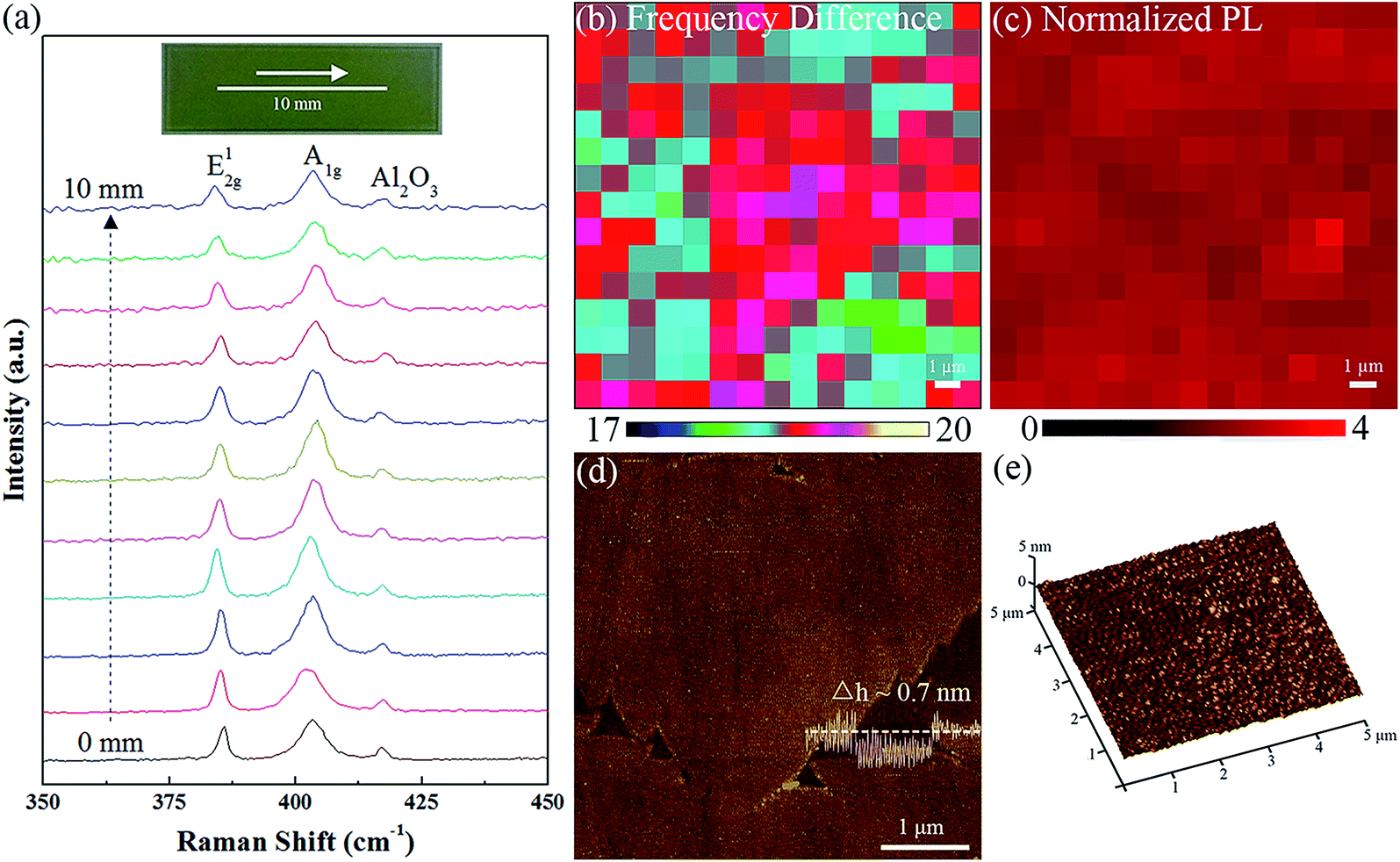 | ||
| Fig. 3 Large-area uniformity of the synthesized monolayer MoS2. (a) Raman spectra of MoS2 film collected every 1 mm along the line as illustrated in the inset. (b and c) Mapping of the Raman frequency difference Δk and normalized PL intensity within a 15 × 15 μm2 area from the monolayer MoS2 film, respectively. (d) AFM image and corresponding section view along the white dash line. (e) Perspective view of a typical AFM image of the as-prepared MoS2 film. | ||
TEM was also applied to investigate the structure of as-made MoS2 film. Fig. 4a is a typical low magnification TEM image of the monolayer MoS2 film, where the folds, cracks, and holes were created during the transfer process. SAED pattern in Fig. 4b shows hexagonal symmetry of the MoS2 structure. Edge folding is a common phenomenon in two-dimensional materials that can be effectively utilized to determine the number of layers.67 We occasionally found folded edges on TEM grid and observed a single dark line in the prepared MoS2 sample (Fig. 4c), which could be correlated to a monolayer. FFT filtered high resolution TEM image in Fig. 4d shows a honeycomb arrangement of atoms with lattice spacing of 2.7 and 1.6 Å, assigning to the (100) and (110) planes, respectively.
 | ||
| Fig. 4 TEM characterizations of monolayer MoS2 film. (a) Low magnification TEM image of MoS2 film. (b) SAED pattern acquired from the area marked with a white dashed circle in (a). (c) High resolution TEM image of the square area in (a). (d) FFT filtered high resolution TEM image of the marked area in (c). | ||
As mentioned above, the reaction process of MoO3 with S involves the stepwise reduction and sulfurization, that is, MoO3 is first partially reduced by vaporized S to form volatile suboxide MoO3−x species, which are further sulfurized to give rise to the formation of MoS2. Sulfur serves as the reductant and sulfurization agent at the same time.55 And it is expected that, in the growth zone along the gas flow direction, MoO3 vapor concentration decreases while S vapor concentration increases. Therefore more distance away from MoO3 precursor, more amount of MoO3 should be reduced and the reduction will be more complete. Meanwhile, MoS2 vapor concentration is anticipated to decrease in the gas flow direction from the region where MoO3 vapor is fully reacted, which would lead to different morphologies of MoS2 on the substrates. To confirm these hypotheses, a series of sapphire substrates were placed successively in the growth zone, as depicted in Fig. 5a. Fig. 5b shows optical microscope images of the products formed at different distance between MoO3 precursor and sapphire substrate (Ddist): when Ddist is less than 10.0 cm, the supply of sulfur is low but sufficient MoO3 is evaporated, little MoO3 is initially reduced and small black particles are nucleated, which are proven to be Mo4O11 by Raman spectrum (Fig. S3†). With the increase of Ddist, rhomboidal shaped MoO2 domains are formed at Ddist = 11.0 cm and become bigger and denser because of the raised sulfur vapor concentration as well as the enhanced reduction. For Ddist = 15.0 cm, parts of the vaporized MoO3 are fully reacted, resulting in the formation of monolayer MoS2 around the MoO2 domains (see Fig. S4† for the larger version of the image and corresponding Raman measurements). When Ddist reaches 16 cm, sulfur is plentiful enough for the full reaction of MoO3 vapor, giving rise to high levels of MoS2 vapor concentration, which in turn causes the simultaneous growth of single- and multi-layered MoS2. As MoS2 vapor concentration reduces along the gas flow direction, multilayer MoS2 domains gets smaller and fewer, and finally disappears at Ddist = 17.5 cm, leaving only the complete monolayer MoS2 film. With the further increase of Ddist, monolayer MoS2 film becomes discontinuous and discrete triangular MoS2 flakes evolve, whose edges are sulfur terminated zigzag ones identified empirically.68 These isolated triangles shrink in size and number, and finally vanish with the cut off of MoS2 supply when Ddist ≥ 19.8 cm. All the results are consistent with the aforementioned hypothesizes and suggest that sulfur vapor flows to growth zone is retarded by Ar gas flow, which moderates MoO3 sulfurization and benefits monolayer MoS2 growth.
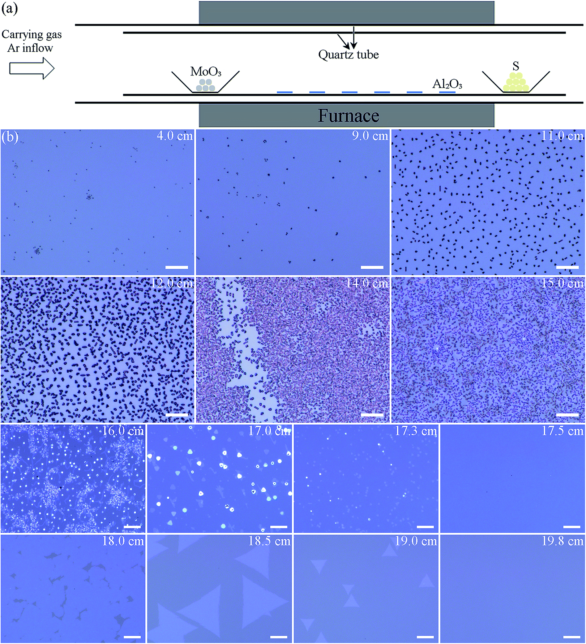 | ||
| Fig. 5 Distance-dependent of products in the CVD growth. (a) Schematic illustration of the successively placed sapphire substrates in the growth zone. (b) Optical microscope images of the products with different MoO3 precursor and sapphire substrate distance (Ddist), as shown on the upper right corner of each image. Scale bars: 10 μm. | ||
It is worth noting that the Ar flow rate would affect readily the sulfur vapor concentration and in turn the resultant MoS2 monolayers. As shown in Fig. 6a–c, when the Ar flow rate is 5 sccm, sulfur vapor concentration is so high that MoO3 vapor is fully reacted before it flows into the growth zone, no products are formed on the sapphire substrates placed in the growth zone. With the increase of Ar flow rate to 30 sccm, sulfur vapor concentration decreases but is still high, irregularly shaped MoS2 monolayers interspersed with bulk MoS2 particles or multilayer patches are formed on the sapphire substrates located at the center of furnace (Ddist = 11.0 cm). Further increase of the Ar flow rate to 300 sccm leads to very low sulfur vapor concentration, which in turn causes the incomplete reaction of MoO3 vapor and the formation of Mo4O11 particles on the sapphire substrates in the growth zone (Fig. S5†). So a proper Ar flow rate is needed for the synthesis of high quality MoS2 monolayers. In our experiment, 50 sccm Ar is appropriate to grow large-area high quality monolayer MoS2 film.
 | ||
| Fig. 6 Influence of Ar flow rate on the resultant MoS2 monolayers. (a–c) Optical microscope images of the products synthesized with different Ar flow rate of 5, 30, and 300 sccm, respectively. Scale bars: 10 μm. | ||
In ref. 45, metal oxide powder (MnO2, V6O13, or Co3O4, etc.) was added to react with extra sulfur at the initial stage of MoO3 reduction to allow MoO2 grow up to microplates, which were used as templates to synthesize MoS2 flakes. Too much sulfur would result in MoS2 particles because the growth of MoO2 was terminated by the complete coverage of MoS2 due to high sulfur vapor concentration. Inspired by the results in Fig. 5 and the fact that sulfur vapor concentration is relatively low in the growth zone for our experiment, we wonder if it is possible to grow MoS2/MoO2 plates on SiO2/Si substrates in configuration Fig. 1b without the need of metal oxides. It is found that like the growth procedure for monolayer MoS2 film, rhomboidal shaped microplates were formed, as seen from Fig. 7a, when SiO2/Si substrates were located at the center of furnace and MoO3 powder was placed 1 cm closer to the center of furnace (the distance between MoO3 powder and SiO2/Si substrates is 10.0 cm) as well as Ar gas flow rate was 20 sccm. Raman spectrum of the as-made microplates in Fig. 7b shows eleven peaks in the range of 150–800 cm−1, which can be assigned to MoS2 (E12g mode ∼ 382 cm−1 and A1g mode ∼ 406 cm−1), MoO2 (∼204, 230, 346, 364, 460, 497, 570, and 743 cm−1),69 and Si (∼520 cm−1). This confirms the rhomboidal shaped microplates to be MoS2/MoO2. Metal oxide powder is not needed to assist the synthesis in our experiment (the Ar flow rate also has an influence on the resultant MoS2/MoO2 microplates, see Fig. S6 in the ESI†).
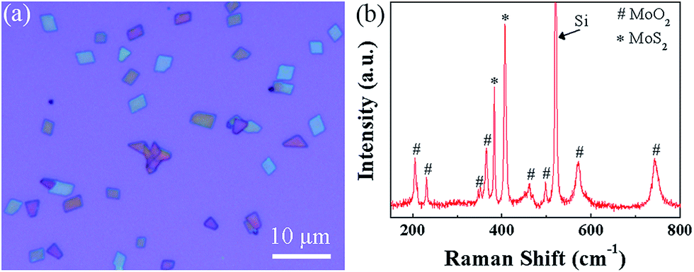 | ||
| Fig. 7 Growth of the MoS2/MoO2 microplates. (a) Optical microscope image and (b) Raman spectrum of the as-synthesized MoS2/MoO2 plates. Peaks marked with ∗ and # correspond to MoS2 and MoO2, respectively. | ||
4. Conclusion
In summary, we present a facile method to grow large-area uniform monolayer MoS2 films via a new CVD configuration. MoO3 is first partially reduced by vaporized S to form volatile suboxide MoO3−x species, which are further sulfurized into MoS2 on the substrate. Mo4O11 particles, MoO2 domains, MoS2 multilayers, monolayer MoS2 film, triangular MoS2 monolayer flakes are successively formed in the growth zone along the gas flow direction. Optical microscope, AFM, Raman and PL mapping show that the as-grown MoS2 films are uniform monolayers over a large area. Meanwhile, FWHM values of Raman and PL peaks of our MoS2 film are close to the exfoliated monolayer sample, indicating the as-grown films are of high quality comparable to the exfoliated MoS2. Rhomboidal shaped MoS2/MoO2 microplates can also be grown using our method without the need of adding metal oxides to assist the synthesis. Moderating MoO3 sulfurization offers an effective way to grow monolayer MoS2 films.Acknowledgements
This work was financially supported by National Basic Research Program of China (Grant No. 2011CB921400 and 2013CB921800), the Natural Science Foundation of China (Grant No. 11374280 and 50772110), and the Natural Science Foundation of Anhui province (Grant No. 1408085ME91).Notes and references
- K. S. Novoselov, A. K. Geim, S. V. Morozov, D. Jiang, Y. Zhang, S. V. Dubonos, I. V. Grigorieva and A. A. Firsov, Science, 2004, 306, 666–669 CrossRef CAS PubMed
.
- A. H. Castro Neto, F. Guinea, N. M. R. Peres, K. S. Novoselov and A. K. Geim, Rev. Mod. Phys., 2009, 81, 109–162 CrossRef CAS
- A. K. Geim and K. S. Novoselov, Nat. Mater., 2007, 6, 183–191 CrossRef CAS PubMed
- A. K. Geim, Science, 2009, 324, 1530–1534 CrossRef CAS PubMed
- D. Garcia-Sanchez, A. M. van der Zande, A. San Paulo, B. Lassagne, P. L. McEuen and A. Bachtold, Nano Lett., 2008, 8, 1399–1403 CrossRef CAS PubMed
- T. O. Wehling, K. S. Novoselov, S. V. Morozov, E. E. Vdovin, M. I. Katsnelson, A. K. Geim and A. I. Lichtenstein, Nano Lett., 2008, 8, 173–177 CrossRef CAS PubMed
- M. D. Stoller, S. J. Park, Y. W. Zhu, J. H. An and R. S. Ruoff, Nano Lett., 2008, 8, 3498–3502 CrossRef CAS PubMed
- T. Palacios, Nat. Nanotechnol., 2011, 6, 464–465 CrossRef CAS PubMed
- K. F. Mak, C. Lee, J. Hone, J. Shan and T. F. Heinz, Phys. Rev. Lett., 2010, 105, 136805 CrossRef PubMed
- A. Splendiani, L. Sun, Y. B. Zhang, T. S. Li, J. Kim, C.-Y. Chim, G. Galli and F. Wang, Nano Lett., 2010, 10, 1271–1275 CrossRef CAS PubMed
- J. Feng, X. Qian, C.-W. Huang and J. Li, Nat. Photonics, 2012, 6, 866–872 CrossRef CAS
- K. He, C. Poole, K. F. Mak and J. Shan, Nano Lett., 2013, 13, 2931–2936 CrossRef CAS PubMed
- A. Castellanos-Gomez, R. Roldán, E. Cappelluti, M. Buscema, F. Guinea, H. S. J. van der Zant and G. A. Steele, Nano Lett., 2013, 13, 5361–5366 CrossRef CAS PubMed
- C. R. Zhu, G. Wang, B. L. Liu, X. Marie, X. F. Qiao, X. Zhang, X. X. Wu, H. Fan, P. H. Tan, T. Amand and B. Urbaszek, Phys. Rev. B: Condens. Matter Mater. Phys., 2013, 88, 121301 CrossRef
- H. Zeng, J. Dai, W. Yao, D. Xiao and X. Cui, Nat. Nanotechnol., 2012, 7, 490–493 CrossRef CAS PubMed
- K. F. Mak, K. He, J. Shan and T. F. Heinz, Nat. Nanotechnol., 2012, 7, 494–498 CrossRef CAS PubMed
- T. Cao, G. Wang, W. Han, H. Ye, C. Zhu, J. Shi, Q. Niu, P. Tan, E. Wang, B. Liu and J. Feng, Nat. Commun., 2012, 3, 887 CrossRef PubMed
- D. Xiao, G.-B. Liu, W. Feng, X. Xu and W. Yao, Phys. Rev. Lett., 2012, 108, 196802 CrossRef PubMed
- G. Sallen, L. Bouet, X. Marie, G. Wang, C. R. Zhu, W. P. Han, Y. Lu, P. H. Tan, T. Amand, B. L. Liu and B. Urbaszek, Phys. Rev. B: Condens.
Matter Mater. Phys., 2012, 86, 081301 CrossRef
- T. F. Jaramillo, K. P. Jørgensen, J. Bonde, J. H. Nielsen, S. Horch and I. Chorkendorff, Science, 2007, 317, 100–102 CrossRef CAS PubMed
- J. Kibsgaard, Z. Chen, B. N. Reinecke and T. F. Jaramillo, Nat. Mater., 2012, 11, 963–969 CrossRef CAS PubMed
- Y. Yu, S.-Y. Huang, Y. Li, S. N. Steinmann, W. Yang and L. Cao, Nano Lett., 2014, 14, 553–558 CrossRef CAS PubMed
- C. Tsai, F. Abild-Pedersen and J. K. Nørskov, Nano Lett., 2014, 14, 1381–1387 CrossRef CAS PubMed
- J. Shi, D. Ma, G.-F. Han, Y. Zhang, Q. Ji, T. Gao, J. Sun, X. Song, C. Li, Y. Zhang, X.-Y. Lang, Y. Zhang and Z. Liu, ACS Nano, 2014, 8, 10196–10204 CrossRef CAS PubMed
- Y. Zhang, Q. Ji, G.-F. Han, J. Ju, J. Shi, D. Ma, J. Sun, Y. Zhang, M. Li, X.-Y. Lang, Y. Zhang and Z. Liu, ACS Nano, 2014, 8, 8617–8624 CrossRef CAS PubMed
- M. A. Lukowski, A. S. Daniel, F. Meng, A. Forticaux, L. Li and S. Jin, J. Am. Chem. Soc., 2013, 135, 10274–10277 CrossRef CAS PubMed
- B. Radisavljevic, A. Radenovic, J. Brivio, V. Giacometti and A. Kis, Nat. Nanotechnol., 2011, 6, 147–150 CrossRef CAS PubMed
- B. Radisavljevic, M. B. Whitwick and A. Kis, ACS Nano, 2011, 5, 9934–9938 CrossRef CAS PubMed
- H. Wang, L. Yu, Y.-H. Lee, Y. Shi, A. Hsu, M. L. Chin, L.-J. Li, M. Dubey, J. Kong and T. Palacios, Nano Lett., 2012, 12, 4674–4680 CrossRef CAS PubMed
- K. S. Novoselov, D. Jiang, F. Schedin, T. J. Booth, V. V. Khotkevich, S. V. Morozov and A. K. Geim, Proc. Natl. Acad. Sci. U. S. A., 2005, 102, 10451–10453 CrossRef CAS PubMed
- Z. Zeng, Z. Yin, X. Huang, H. Li, Q. He, G. Lu, F. Boey and H. Zhang, Angew. Chem., Int. Ed., 2011, 50, 11093–11097 CrossRef CAS PubMed
- J. N. Coleman, M. Lotya, A. O'Neill, S. D. Bergin, P. J. King, U. Khan, K. Young, A. Gaucher, S. De, R. J. Smith, I. V. Shvets, S. K. Arora, G. Stanton, H.-Y. Kim, K. Lee, G. T. Kim, G. S. Duesberg, T. Hallam, J. J. Boland, J. J. Wang, J. F. Donegan, J. C. Grunlan, G. Moriarty, A. Shmeliov, R. J. Nicholls, J. M. Perkins, E. M. Grieveson, K. Theuwissen, D. W. McComb, P. D. Nellist and V. Nicolosi, Science, 2011, 331, 568–571 CrossRef CAS PubMed
- K.-G. Zhou, N.-N. Mao, H.-X. Wang, Y. Peng and H.-L. Zhang, Angew. Chem., Int. Ed., 2011, 50, 10839–10842 CrossRef CAS PubMed
- A. Castellanos-Gomez, M. Barkelid, A. M. Goossens, V. E. Calado, H. S. J. Van der Zant and G. A. Steele, Nano Lett., 2012, 12, 3187–3192 CrossRef CAS PubMed
- Y. Liu, H. Nan, X. Wu, W. Pan, W. Wang, J. Bai, W. Zhao, L. Sun, X. Wang and Z. Ni, ACS Nano, 2013, 7, 4202–4209 CrossRef CAS PubMed
- K.-K. Liu, W. J. Zhang, Y.-H. Lee, Y.-C. Lin, M.-T. Chang, C.-Y. Su, C.-S. Chang, H. Li, Y. M. Shi, H. Zhang, C.-S. Lai and L.-J. Li, Nano Lett., 2012, 12, 1538–1544 CrossRef CAS PubMed
- A. S. George, Z. Mutlu, R. Ionescu, R. J. Wu, J. S. Jeong, H. H. Bay, Y. Chai, K. A. Mkhoyan, M. Ozkan and C. S. Ozkan, Adv. Funct. Mater., 2014, 24, 7461–7466 CrossRef CAS
- Y. J. Zhan, Z. Liu, S. Najmaei, P. M. Ajayan and J. Lou, Small, 2012, 8, 966–971 CrossRef CAS PubMed
- Y. B. Lee, J. Lee, H. Bark, I.-K. Oh, G. H. Ryu, Z. Lee, H. Kim, J. H. Cho, J.-H. Ahn and C. G. Lee, Nanoscale, 2014, 6, 2821–2826 RSC
- N. Choudhary, J. Park, J. Y. Hwang and W. Choi, ACS Appl. Mater. Interfaces, 2014, 6, 21215–21222 CAS
- Y.-C. Lin, W. J. Zhang, J.-K. Huang, K.-K. Liu, Y.-H. Lee, C.-T. Liang, C.-W. Chu and L.-J. Li, Nanoscale, 2012, 4, 6637–6641 RSC
- S. Wu, C. Huang, G. Aivazian, J. S. Ross, D. H. Cobden and X. Xu, ACS Nano, 2013, 7, 2768–2772 CrossRef CAS PubMed
- L. K. Tan, B. Liu, J. H. Teng, S. F. Guo, H. Y. Low and K. P. Loh, Nanoscale, 2014, 6, 10584–10588 RSC
- Z. Jin, S. Shin, D. H. Kwon, S.-J. Han and Y.-S. Min, Nanoscale, 2014, 6, 14453–14458 RSC
- X. Wang, H. Feng, Y. Wu and L. Jiao, J. Am. Chem. Soc., 2013, 135, 5304–5307 CrossRef CAS PubMed
- Y. F. Yu, C. Li, Y. Liu, L. Q. Su, Y. Zhang and L. Y. Cao, Sci. Rep., 2013, 3, 1866 Search PubMed
- J. Jeon, S. K. Jang, S. M. Jeon, G. Yoo, Y. H. Jang, J.-H. Park and S. Lee, Nanoscale, 2015, 7, 1688–1695 RSC
- Y.-H. Lee, X.-Q. Zhang, W. J. Zhang, M.-T. Chang, C.-T. Lin, K.-D. Chang, Y.-C. Yu, J. T.-W. Wang, C.-S. Chang, L.-J. Li and T.-W. Lin, Adv. Mater., 2012, 24, 2320–2325 CrossRef CAS PubMed
- S. Najmaei, Z. Liu, W. Zhou, X. Zou, G. Shi, S. Lei, B. I. Yakobson, J.-C. Idrobo, P. M. Ajayan and J. Lou, Nat. Mater., 2013, 12, 754–759 CrossRef CAS PubMed
- X. Ling, Y.-H. Lee, Y. Lin, W. Fang, L. Yu, M. S. Dresselhaus and J. Kong, Nano Lett., 2014, 14, 464–472 CrossRef CAS PubMed
- J. Zhang, H. Yu, W. Chen, X. Tian, D. Liu, M. Cheng, G. Xie, W. Yang, R. Yang, X. Bai, D. Shi and G. Zhang, ACS Nano, 2014, 8, 6024–6030 CrossRef CAS PubMed
- Q. Ji, Y. Zhang, T. Gao, Y. Zhang, D. Ma, M. Liu, Y. Chen, X. Qiao, P.-H. Tan, M. Kan, J. Feng, Q. Sun and Z. Liu, Nano Lett., 2013, 13, 3870–3877 CrossRef CAS PubMed
- D. Dumcenco, D. Ovchinnikov, K. Marinov, P. Lazić, M. Gibertini, N. Marzari, O. L. Sanchez, Y.-C. Kung, D. Krasnozhon, M.-W. Chen, S. Bertolazzi, P. Gillet, A. F. i. Morral, A. Radenovic and A. Kis, ACS Nano, 2015, 9, 4611–4620 CrossRef CAS PubMed
- Q. Ji, M. Kan, Y. Zhang, Y. Guo, D. Ma, J. Shi, Q. Sun, Q. Chen, Y. Zhang and Z. Liu, Nano Lett., 2015, 15, 198–205 CrossRef CAS PubMed
- X. L. Li and Y. D. Li, Chem.–Eur. J., 2003, 9, 2726–2731 CrossRef CAS PubMed
- Z. Y. Zhu, Y. C. Cheng and U. Schwingenschlögl, Phys. Rev. B: Condens. Matter Mater. Phys., 2011, 84, 153402 CrossRef
- K. F. Mak, K. He, C. Lee, G. H. Lee, J. Hone, T. F. Heinz and J. Shan, Nat. Mater., 2013, 12, 207–211 CrossRef CAS PubMed
- M. Buscema, G. A. Steele, H. S. J. van der Zant and A. Castellanos-Gomez, Nano Res., 2014, 7, 561–571 CrossRef
- Y. Y. Li, Z. M. Qi, M. Liu, Y. Y. Wang, X. R. Cheng, G. B. Zhang and L. S. Sheng, Nanoscale, 2014, 6, 15248–15254 RSC
- S. Ghatak, A. N. Pal and A. Ghosh, ACS Nano, 2011, 5, 7707–7712 CrossRef CAS PubMed
- W. Zhu, T. Low, Y.-H. Lee, H. Wang, D. B. Farmer, J. Kong, F. Xia and P. Avouris, Nat. Commun., 2014, 5, 3087 Search PubMed
- M. Amani, M. L. Chin, A. L. Mazzoni, R. A. Burke, S. Najmaei, P. M. Ajayan, J. Lou and M. Dubey, Appl. Phys. Lett., 2014, 104, 203506 CrossRef
- H. Schmidt, S. Wang, L. Chu, M. Toh, R. Kumar, W. Zhao, A. H. C. Neto, J. Martin, S. Adam, B. Özyilmaz and G. Eda, Nano Lett., 2014, 14, 1909–1913 CrossRef CAS PubMed
- Z. C. Feng, A. Mascarenhas and W. J. Choyke, J. Lumin., 1986, 35, 329–341 CrossRef CAS
- T. Schmidt, K. Lischka and W. Zulehner, Phys. Rev. B: Condens. Matter Mater. Phys., 1992, 45, 8989–8994 CrossRef
- V. Senthilkumar, L. C. Tam, Y. S. Kim, Y. Sim, M.-J. Seong and J. I. Jang, Nano Res., 2014, 7, 1759–1768 CrossRef CAS
- J. C. Meyer, A. K. Geim, M. I. Katsnelson, K. S. Novoselov, T. J. Booth and S. Roth, Nature, 2007, 446, 60–63 CrossRef CAS PubMed
- A. M. van der Zande, P. Y. Huang, D. A. Chenet, T. C. Berkelbach, Y. You, G.-H. Lee, T. F. Heinz, D. R. Reichman, D. A. Muller and J. C. Hone, Nat. Mater., 2013, 12, 554–561 CrossRef CAS PubMed
- M. Dieterle and G. Mestl, Phys. Chem. Chem. Phys., 2002, 4, 822–826 RSC
Footnote |
| † Electronic supplementary information (ESI) available: Optical microscope images of MoS2 synthesized in configuration Fig. S1a, optical microscope image and atomic force microscope image of the exfoliated monolayer MoS2 sample, Raman measurements of the intermediate oxides, and optical microscope images as well as Raman measurements of the products synthesized with different Ar flow rate. See DOI: 10.1039/c6ra03641d |
| This journal is © The Royal Society of Chemistry 2016 |