DOI:
10.1039/C6RA03630A
(Paper)
RSC Adv., 2016,
6, 46231-46237
Electrical characterization and conductivity optimization of laser reduced graphene oxide on insulator using point-contact methods
Received
8th February 2016
, Accepted 27th April 2016
First published on 28th April 2016
Abstract
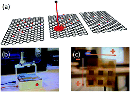
The present work is focused on the electrical characterization of laser-assisted reduced graphene oxide by point-contact techniques. The aim is twofold: firstly, the careful investigation of in-line two and four point-contact techniques applied to macroscopic samples of reduced graphene oxide. The combination of both methods has shed light on the role of the point-contact when extracting the intrinsic resistivity of the material. Secondly, once the measurement protocol is well understood, it is applied to improve the conductivity of the samples by the adjustment of the initial colloid concentration and the photothermal power intensity used for the reduction. The final optimized samples present promising conductivity, comparable to that of large graphene sheets obtained by chemical vapor deposition methods.
1 Introduction
Beyond any doubt, graphene has stirred the world of material research due to its unique physical properties.1–3 In particular, in the field of electronics, always constrained by the scaling race and new integration paradigms of semiconductor devices, graphene has found a huge niche of interest.4 However, the expectations have not been yet materialized into real-world applications due, in part, to the difficulty to produce and pattern large graphene samples. The efficient fabrication of graphene layers is a critical process to achieve the expected properties at a reasonable cost. The industrial methods for producing high quality samples, beyond the experimental approach based on ‘Scotch-taping’,5 mainly involve high temperature vacuum annealing of silicon carbide6 or Chemical Vapor Deposition (CVD).7 Despite the repeatability of those methods being more than proven and the quality of the samples well demonstrated, it is also true that those methods do not fully satisfy yet the requirements for cost-effective circuit integration.
Not far from the bellwether research activity related to graphene and its two-dimensional counterparts,8 the interest around a poorer form of graphene, so called reduced graphene oxide (rGO), has gained a lot of relevance due to its multiple spectrum of applications at a much lower technological effort.9–12 Although it is far from achieving the unique properties of graphene, rGO preserves, to some extent, part of its merits (flexibility, electrical and thermal conductivity, etc.).13 But the most appealing advantage of laser-assisted photothermal reduced graphene oxide is the possibility to create large precise conductive patterns (rGO) electrically isolated by the unexposed graphene oxide areas (GO), escaping from the need for lithographic masks.
This work provides insights on the considerations that must be addressed to carry out simple point-contact measurements on the bare rGO films. Once the basics are established, the methodology is applied for optimization, in terms of the electrical conductivity, of the synthesized samples. The paper is divided in two blocks: Section 2 summarizes the conditions under which the rGO samples have been obtained and describes the experimental methodology followed for their point-contact electrical characterization. The spectroscopic and electrical results, as well as the path for the optimization of the samples, are documented in Section 3, including benchmarking with commercial graphene obtained by chemical vapor deposition. Finally, the main conclusions are drawn in Section 4.
2 Sample preparation and experimental setup
Graphene oxide has been obtained following a modified version of the Hummers and Offeman method14 based on the oxidation and exfoliation of natural graphite powder through sonication in a water dispersion. This procedure yields a homogeneous dispersion, indefinitely stable, containing primarily monolayer sheets (graphene oxide). The hydrophilic nature of graphene oxide implies that water molecules can easily intersperse in the graphite oxide, causing the layer splitting.15
Graphene oxide behaves as an electrical insulator due to the alteration suffered by the carbon atoms during the oxidation process (GO has sp2 and sp3 hybridized carbon atoms). The electrical conductivity can be recovered easily removing the functional groups and thus partially restoring the original sp2 electronic structure. Thermal annealing and hydrazine vapor reduction of GO are the two most commonly used methods to directly get conductive rGO films.16 However, the search for safe and ecological procedures to reduce GO points to photothermal reduction assisted by a laser as one of the most efficient processes2,17 (Fig. 1a).
 |
| Fig. 1 (a) Illustration of GO reduction with laser diode irradiation according to the Lerf–Klinowski model.18 Before graphene oxide thermal reduction, there is a large amount of functional hydroxyl (C–OH) and epoxyl (C–O–C) groups (left). The functional groups are broken during the reduction process (center) for obtaining the partial restoration of the graphene layers, although some defects remain in the structure (right). (b) Image of the experimental setup based on a numerical control unit with interchangeable laser head. (c) An example of 1 cm × 1 cm rGO samples on a PET substrate reduced at increasing laser power intensities from 65 mW to 105 mW with an increment of 5 mW in the direction of the arrows. | |
For our experiments, we synthesized 1 L of 4 mg mL−1 GO colloid. Different quantities of the dispersion were deposited on 3M® 100 μm-thin polyethylene terephthalate (PET) films and SiO2/Si substrates (90 nm SiO2 on highly P-type doped Si). After GO deposition, the films were left inside a class 10 cabinet on a 3D-shaker at room temperature until water was completely evaporated.
The laser-assisted photothermal reduction process was carried out by an ad hoc laser setup mounted on a motorized in-plane platform, allowing a spacial resolution of about 20 μm and an effective excursion surface up to 100 cm2 (Fig. 1b). Two laser heads were available: the first laser features a fixed power of 4.7 mW at a wavelength of 788 nm, whereas the second system features the same mechanical characteristics with a adjustable laser power from approximately 15 mW up to 250 mW at a wavelength of 550 nm. The reason for using different laser sources and power intensities was to study the correlation between laser power and excursion speed during the reduction process, as well as to verify the effective reduction at different wavelengths.
The samples fabricated for the experiments consisted of 1 cm × 1 cm rGO squares (laterally isolated by GO) deposited on top of the PET film or on SiO2/Si substrates. The process started by pouring the GO colloid on a PET film (equivalent GO colloid surface concentration 100 μL cm−2). Then, 1 cm × 1 cm squares were developed by reducing the GO surface under different laser power. An example of a sample on a PET substrate is shown in Fig. 1c. As the GO gets more efficiently reduced, the film turns from a brownish transparent color to a dark-brown color, symptomatic of the recovery of the graphitic structures.
The next objective of this work was focused on the standardization of fast and reliable electrical characterization procedures for large macroscopic samples. We centered our attention on point-contact methods to characterize the intrinsic conductivity of the material, since these procedures constitute one of the fastest approaches for monitoring the electrical properties of the samples. The experimental setup is based on the in-line point-contact configuration19 with the direct contact of pressure-adjustable tungsten-carbide (WC) probes or ad hoc deposited Ag contacts (the probes are placed on top of the Ag in this latter case). Two alternative measurement configurations were considered (Fig. 2):
 |
| Fig. 2 (a) Four point-contact setup, current I is forced between probes 1 and 4 by applying a constant bias V1–4 while the voltage drop is measured between probes 2 and 3. (b) Two point-contact setup, current I and voltage V are simultaneously applied and measured through the same probes (2 and 3). | |
(i) Four point-contact setup (4PC): a voltage is applied between probes 1 and 4 (V1–4) while the current, I, is simultaneously measured (see Fig. 2a). The voltage difference between probes 2 and 3 (V2–3) is simultaneously monitored without current flow through them (and therefore, without voltage drop due to contact resistance). The resistance R4p = V2–3/I obtained with this configuration can be related to the sheet resistance (Rsh) by the relationship Rsh = FR4p, where F is a form factor depending on the sample dimensions and position of the probes.19 This technique is sometimes also referred as the Kelvin method.20
(ii) Two point-contact setup (2PC): a voltage is applied between probes 2 and 3 (V2–3) while the current flow through them is simultaneously measured (Fig. 2b). This type of measurement is easier to be carried out, since there is no need to take precautions regarding probe alignment, but it is affected by the impact of the contact resistance which can eventually mask the intrinsic conductivity of the sample under study.21 Note also that even in the case that the contact resistance could be neglected, the resistance measured by the first method may not correspond to the value given by V2–3/I2–3 due to the current spreading. Nevertheless, the two point-contact method represents a good procedure to determine the contact resistance (distance-dependent two-point probe method).22,23
3 Results and discussion
3.1 Spectroscopic characterization of laser-reduced graphene oxide
The effectiveness of the reduction process was confirmed by Raman spectroscopy (JASCO NRS-5100). This powerful and non-invasive technique can provide a large amount of information of the crystal structure related to disorder, defects, and thickness.24,25 The reduction process of GO can manifest itself in Raman spectra by the changes in the relative intensity of two main peaks: D and G.26 An example is shown in Fig. 3. In the GO Raman spectrum (Fig. 3a), the D and G peaks are located at 1352 cm−1 and 1600 cm−1 respectively; the 2D peak is almost non-existent. After the reduction process (Fig. 3b and c), the D peak (related to defects and crystal distortion) is attenuated (the IG/ID ratio increases from ≃1 to >1.6), and the 2D peak emerges with a large intensity, which is a consequence of the partial restoration of the crystallographic structure and the reduction of the number of defects. The ID/IG values achieved after the reduction together with the sharpness of the peaks suggest that a thermal annealing process takes place on the rGO surface, partially healing the graphene layers.27 The low I2D/IG ratio, and the relatively wide Full Width at Half Maximum (FWHM) (taking values from 80 to 100 cm−1) reveal the multilayer nature of the samples.25 The better ratios in Fig. 3c, achieved despite using a lower photothermal reduction power, are due to a slower speed excursion.
 |
| Fig. 3 Raman spectra of different samples on PET substrates: (a) GO before reduction, (b) reduced-GO at a laser power of 100 mW (λ = 550 nm) at an excursion rate of 1 min cm−2, (c) reduced-GO at a laser power of 5 mW (λ = 788 nm) at an excursion rate of 24 min cm−2. | |
The elemental composition analysis was carried out by fundamental X-ray photoelectron spectroscopy (XPS, Kratos Axis Ultra-DLD), providing information about the relative levels of oxidation, C/O ratios and the chemical environment of atoms. All spectra were calibrated with the position of the C–C peak at 284.6 ± 0.4 eV. Fig. 4a shows XPS spectra obtained from GO and rGO samples on SiO2 and on PET substrates. The analysis of the area of C1s and O1s spectrum peaks provides atomic carbon to oxygen ratios (C/O) of 2.27 for GO, 3.61 for rGO on SiO2 and 6.36 for rGO on PET. The larger C/O ratio on the PET substrates is attributed to the different thermal conductivity of the substrates (∼0.2 W m−1 K−1 for PET, ∼1.5 W m−1 K−1 for SiO2). The poor heat dissipation of PET yields a more localized heat spot, favoring the reduction process, whereas the better heat dissipation of the SiO2 substrate lessens the effectiveness in the reduction process. Fig. 4b shows the C1s spectra from the same samples of Fig. 4a. Each spectrum is deconvoluted (CasaXPS software) into four peaks corresponding to the following functional groups: carbon sp2 and sp3 (C), epoxy and hydroxyls (C–O), carbonyl (C
O) and carboxylates (O–C
O).28 The laser reduction process decreases the oxygen-containing functional groups and recovers the carbon configurations (sp2), confirming the results from Raman spectroscopy.
 |
| Fig. 4 XPS spectra for graphene oxide and reduced graphene oxide on PET and SiO2 substrates: (a) comparison of wide spectra, (b) comparison of C1s peaks. The initial GO concentration before water evaporation was 70 μL cm−2; the laser power was 90 mW (1 cm2 min−1). | |
3.2 Electrical characteristics of laser-reduced graphene oxide
Prior to the measurement phase, the impact of the probe pressure on the GO surface was investigated. This initial precaution is mandatory for the 2PC setup since, as stated before, the value of conductance extracted may be largely affected by the contact resistance. Fig. 5 shows the normalized conductance when performing 2PC measurements sequentially on the same area, as a function of the WC probes load (tip radius 25 μm). Two samples were prepared: the first one on a PET substrate and the second on SiO2, both starting with the same initial concentration of colloid and reduced under the same conditions. For the case of the rGO on PET, the conductivity increases monotonically until saturation is achieved for a load larger than 60 g. This relationship between contact improvement and probe pressure can be related to the large number of interface states created by the damage of the probe contact (amplified when increasing the probe pressure): the imperfections and induced dislocations shunt the space-charge layer, the electric field is concentrated at the edges of the probes and the current flow is owing to a field emission mechanism.29 Additionally, due to the large number of crystal-lattice defects near the contact, the lifetime of charge carriers is extremely short in this region, so that an ohmic contact is formed due to recombination of charge carriers.29 The situation with the rGO on SiO2 is rather different: the relative conductance increases abruptly achieving a maximum at a load of only 20 g and then starts to decrease for increasing loads. The different behavior is related to the nature of the hard SiO2 substrate itself and a consequence of the measurement procedure. The curves in Fig. 5 are obtained by successively placing the needles on the same contact points, so cumulative damage is induced easily on the harder substrate. The soft PET substrate can absorb the needle pressure more easily, lessening the surface damage by the substrate damping. Note that there is a large difference between the Young modulus of both substrates: ∼70 GPa for SiO2 and ∼2.5 GPa for PET. This degradation phenomenon is not observed when positioning the probes on virgin surface areas; in that case, the conductivity of rGO on SiO2 saturates for a probe load over 20–30 g. An example of the crater created by the needle using a SiO2 substrate is shown in the inset of Fig. 5. All the point-contact experiments carried out on this work were performed contacting a virgin surface at a load of 70 g for the 2PC setup, or 30 g for 4PC or deposited Ag setups.
 |
| Fig. 5 Relative conductance extracted by successive 2PC measurements and direct WC contact as a function of the probe load for rGO reduced on PET and SiO2 substrates. Inset: microscope image of the probe crater generated by the probe. | |
Typical resistance characteristics of the reduced graphene oxide are shown in Fig. 6a. As observed, there is a large discrepancy between the 2PC and 4PC characterization methods. We first focus on the results for 2PC. The direct contact of the WC probes on the surface yields a large value of the resistance, well above the kΩ range. The value is reduced down to 190 Ω when the two point-contact measurement is carried out through deposited Ag contacts. In addition, the direct contact measurement exhibits a remarkable voltage dependence, revealing the nature of the field emission mechanism.30 The difference between the values of resistance extracted using direct WC contacts and the deposited Ag contacts in Fig. 6a lies in the contact resistance, which is dramatically high for the first case. An example of contact resistance extraction is provided in Fig. 6b. This figure is obtained by extracting the total resistance for several probe distances and then extrapolating it to zero probe interdistance. The residual resistance at d = 0 corresponds to the average resistance of probes 1 and 2, Rc1 + Rc2 ≈ 2Rc = 93 Ω.31 The resulting contact resistance, for one single probe contacting the sample with a deposited Ag contact, is Rc = 46.5 Ω. This value is much lower than that of the WC direct contact case (well above the kΩ range, which would advise against its use), but still not low enough to disclose the intrinsic properties of the rGO, as the 4PC measurements will reveal. Note that this contact resistance extraction procedure is valid as long as the form factor of the current flow remains invariant with the probe distance (large rGO sample compared with the needle separation, guaranteeing a linear relationship between the total two point-contact resistance, R2PC, and the needle separation, d).19
 |
| Fig. 6 (a) Comparison of resistance extracted from 4 and 2 point-contact measurements combining direct contact of the rGO surface with the WC probes and deposited Ag contacts. (b) Example of contact resistance extraction for Ag deposited contacts by extrapolation of the 2 point-contact resistance at d = 0. The residual contact resistance is relatively low compared to that of direct WC contacts, explaining the differences observed in (a). (c) Sheet resistance as a function of applied voltage for a 1 cm × 1 cm reduced graphene oxide sample on a SiO2 substrate with Ag deposited contacts covering opposite edges of the sample (open symbols), and 4PC measurements with direct contact of the WC probes on the rGO surface and through silver contacts (lines). | |
4PC measurements, shown by the open squares and open triangular symbols in Fig. 6a, yield a lower value of total resistance (≈80 Ω). As exposed before, this value is not directly comparable with the 2PC value since the current flow covered by the voltage measurement differs in both cases.20 However, the fundamental message, in terms of the standardization of the characterization protocols, is to notice how the value of resistance extracted by the 4PC method remains the same regardless of the contact approach, suppressing effectively the undesirable role of the contact resistance which is masking the intrinsic properties of the material. Notice how both 4PC curves (direct WC contact and Ag contact) yield the same resistance results in Fig. 6c.
The corresponding extracted values of sheet resistance are shown in Fig. 6c. Those values are obtained by multiplying the resistance by the current form factor, accounting for the sample size, and position of the probes. A detailed description of this factor can be found in the literature.19,32 The value of the sheet resistance for the sample considered in Fig. 6c is 360 Ω sq−1. Despite both WC point-contact and Ag deposited contact generate the same value of sheet resistance, at the magnified resistance scale of Fig. 6c, the direct point-contact leads to a much more noisy measurement, as a consequence of the large number of defects generated by the needles over the the rGO contact surface. Finally, we have extracted the sheet resistance, making use of its implicit definition (the resistance of a square). Ag contacts were deposited along the opposite side edges of a 1 cm × 1 cm rGO sample. This non-Kelvin measurement yields a value of sheet resistance of 453 Ω sq−1, about 25% larger than the one obtained by the 4PC measurement. Note that this difference corresponds, basically, with the contact resistance previously extracted (Fig. 6b).
3.3 Initial surface GO concentration and laser power dependencies
During the reduction process, both the laser power and the amount of deposited GO influence the electrical properties of the resulting rGO film. The impact of the initial surface concentration of GO dispersion over the PET surface on the sheet resistance is shown in Fig. 7a. As observed, the values of sheet resistance are scattered depending on the concentration; however, we can notice that, overall, the higher the concentration, the higher the sheet resistance after the reduction. This statement must be qualified for the extreme cases. For concentrations above 150 μL cm−2 the sheet resistance is saturated at values approximately in the range from 600 Ω sq−1 to 800 Ω sq−1 (90 mW laser power case). On the opposite side, we did not see any improvement when reducing the concentration below 80 μL cm−2. Actually, there is a point (at around 20 μL cm−2, not shown in Fig. 7a) where the homogeneity of the samples becomes compromised and the characterization becomes ambiguous since the sheet resistance jumps to large values (over kΩ). We consider that the origin of the observed behavior (at low concentration) lies in the difficulty to aggregate different flakes and therefore to restore (partially) the continuity of the polycrystalline structure of the sample by the photothermal treatment. On the other side, for higher concentrations, only the initial layers are effectively reduced by the photothermal treatment (confirmed by mechanical exfoliation), and therefore, the improvement of the conductivity becomes saturated.
 |
| Fig. 7 (a) Sheet resistance extracted using 4PC method for 1 cm × 1 cm samples with different initial graphene concentration (before water evaporation) for two different laser powers. (b) Sheet resistance of the rGO obtained with an initial surface concentration of colloid of 70 μL cm−2 as a function of the laser power (λ = 550 nm). Laser power above 120 mW can compromise the integrity of the PET substrate at a laser excursion speed of 1 cm2 min−1. | |
The laser power was controlled externally by a programmable power supply adjusting the laser power intensity from 30 to 250 mW (λ = 550 nm). Fig. 7b presents results of the sheet resistance as a function of the laser power intensity. The increase in the photothermal intensity during the reduction process boosts the conductivity, lowering the sheet resistance down to the promising value of 226 Ω sq−1. The non-linear relationship between both magnitudes (sheet resistance and laser power) eventually ends up with saturation of the conductivity increase. Above 95 mW, at an excursion rate of 1 cm2 min−1, the increase of conductivity (decrease of resistivity) is marginal. Further power increase must be carried out with caution since it may fall outside the safe operating area of the PET substrate in terms of local heating.
3.4 Temperature dependence
Electrical resistivity measurements were performed for rGO samples on SiO2 substrates from 300 K to 400 K under high vacuum conditions (10−5 mbar, Janis ST-500 cryostat). In this temperature range, the samples are characterized by non-metallic linear behavior.33 Both 2PC (deposited Ag contacts at the opposite edge of the sample) and 4PC (Ag deposited contacts) configurations were analyzed. The experimental data in Fig. 8 show that the trend is the same regardless of the measurement configuration, the contact resistance being the only factor responsible for the shift of the curves. The fact that the slope of the Rsh(T) curve in the 2PC configuration is the same as in the 4PC setup further confirms the hypothesis of the field emission as the primary injection mechanism.
 |
| Fig. 8 Sheet resistance (Rsh) as a function of temperature in two point-contact (2PC) and four point-contact (4PC) configurations. For the first case, the contact is carried out through deposited Ag electrodes covering two opposite edges of the sample, whereas for the 4PC case, the contact is done with the WC probes on Ag deposited electrodes. | |
The experimental values of the resistance were extracted both during the heating and cooling of the samples, verifying the lack of any hysteresis effect. This linear R–T dependence of rGO has been studied by Sahoo et al. regarding possible thermistor applications.34
3.5 Sample comparison
We finished this study by comparing the sheet resistance of our rGO samples (under the best reduction conditions in terms of initial colloid concentration and laser power) with that of macroscopic graphene samples produced by chemical vapor deposition methods7 acquired from different vendors on SiO2 and PET substrates. The results have been summarized in Fig. 9. The sheet resistance has been extracted with the 4PC configuration described in Section 2. The values of sheet resistance extracted are well aligned with those provided by the vendors for commercial CVD graphene transferred to isolating substrates (typically ranging from 500 Ω sq−1 to 1000 Ω sq−1). The more stunning message here is the good value of the sheet resistance obtained from the rGO samples, surpassing those of the CVD samples. This result reflects the benefits of the laser reduced GO (in terms of conductivity) once the procedure is optimized, and paves the way for its further exploration in different fields of electronics where large, flexible, inexpensive and easy patterned conductive films are needed.
 |
| Fig. 9 Comparison of the sheet resistance, Rsh, extracted by the 4PC method from CVD graphene on PET and SiO2 substrates acquired from commercial channels and optimized rGO samples. Characterization of two CVD samples on SiO2 from the same vendor (vendor 2) reflects the variability of the commercial samples. | |
4 Conclusion
Point-contact electrical characterization techniques have been demonstrated as a fast and reliable approach to extract the electrical properties of large macroscopic samples of laser reduced graphene oxide. The advantages and drawbacks of four point-contact and two point-contact configurations have been highlighted, revealing the severe impact of the contact on the electrical characteristics. These methods have also provided valuable feedback for the optimization of the photothermically assisted reduction process, allowing the selection of the best trade-off between the initial colloid concentration and laser power during the reduction process. The experiments have shown that the lower the GO concentration, the better the electrical conductivity, as far as that the homogeneity of the layer is not compromised. On the other side, increasing the laser power intensity initially benefits the conductivity of the reduced samples before achieving a saturation regime. Against all odds, the optimized rGO samples present promising values of electrical conductivity, competing with those of large commercial CVD samples.
Acknowledgements
The authors would like to thank BBVA-Spain Foundation for the “Ayudas para Investigadores y Creadores Culturales” program, CIC-UGR, CEMIX-UGR and regional government through the P12-TIC-1996 project for supporting this work.
References
- A. C. Ferrari, F. Bonaccorso, V. Falko, K. S. Novoselov, S. Roche, P. Boggild, S. Borini, F. Koppens, V. Palermo, N. Pugno, J. A. Garrido, R. Sordan, A. Bianco, L. Ballerini, M. Prato, E. Lidorikis, J. Kivioja, C. Marinelli, T. Ryhänen, A. Morpurgo, J. N. Coleman, V. Nicolosi, L. Colombo, A. Fert, M. Garcia-Hernandez, A. Bachtold, G. F. Schneider, F. Guinea, C. Dekker, M. Barbone, C. Galiotis, A. Grigorenko, G. Konstantatos, A. Kis, M. Katsnelson, C. W. J. Beenakker, L. Vandersypen, A. Loiseau, V. Morandi, D. Neumaier, E. Treossi, V. Pellegrini, M. Polini, A. Tredicucci, G. M. Williams, B. H. Hong, J. H. Ahn, J. M. Kim, H. Zirath, B. J. van Wees, H. van der Zant, L. Occhipinti, A. Di Matteo, I. a. Kinloch, T. Seyller, E. Quesnel, X. Feng, K. Teo, N. Rupesinghe, P. Hakonen, S. R. T. Neil, Q. Tannock, T. Löfwander and J. Kinaret, Nanoscale, 2014, 7, 4598–4810 RSC.
- M. F. El-Kady, V. Strong, S. Dubin and R. B. Kaner, Science, 2012, 335, 1326–1330 CrossRef CAS PubMed.
- H. Alcalde, J. de la Fuente, B. Kamp and A. Zurutuza, Proc. IEEE, 2013, 101, 1793–1800 CrossRef.
- G. Lu, K. Yu, Z. Wen and J. Chen, Nanoscale, 2013, 5, 1353 RSC.
- K. S. Novoselov, A. K. Geim, S. V. Morozov, D. Jiang, Y. Zhang, S. V. Dubonos, I. V. Grigorieva and A. A. Firsov, Science, 2004, 306, 666–669 CrossRef CAS PubMed.
- C. Berger, Z. Song, X. Li, X. Wu, N. Brown, C. Naud, D. Mayou, T. Li, J. Hass, A. N. Marchenkov, E. H. Conrad, P. N. First and W. A. de Heer, Science, 2006, 312, 1191–1196 CrossRef CAS PubMed.
- A. Reina, X. Jia, J. Ho, D. Nezich, H. Son, V. Bulovic, M. S. Dresselhaus and K. Jing, Nano Lett., 2009, 9, 30–35 CrossRef CAS PubMed.
- A. K. Geim and K. S. Novoselov, Nat. Mater., 2007, 6, 183–191 CrossRef CAS PubMed.
- B. Zhao, P. Liu, Y. Jiang, D. Pan, H. Tao, J. Song, T. Fang and W. Xu, J. Power Sources, 2012, 198, 423–427 CrossRef CAS.
- J. T. Robinson, F. K. Perkins, E. S. Snow, Z. Wei and P. E. Sheehan, Nano Lett., 2008, 8, 3137–3140 CrossRef CAS PubMed.
- H. A. Becerril, J. Mao, Z. Liu, R. M. Stoltenberg, Z. Bao and Y. Chen, ACS Nano, 2008, 2, 463–470 CrossRef CAS PubMed.
- J. T. Robinson, M. Zalalutdinov, J. W. Baldwin, E. S. Snow, Z. Wei, P. Sheehan and B. H. Houston, Nano Lett., 2008, 8, 3441–3445 CrossRef CAS PubMed.
- G. Eda, G. Fanchini and M. Chhowalla, Nat. Nanotechnol., 2008, 3, 270–274 CrossRef CAS PubMed.
- J. William, S. Hummers and R. E. Offeman, J. Am. Chem. Soc., 1958, 80, 1339 CrossRef.
- M. Hirata, T. Gotou, S. Horiuchi, M. Fujiwara and M. Ohba, Carbon, 2004, 42, 2929–2937 CAS.
- S. Stankovich, D. A. Dikin, R. D. Piner, K. A. Kohlhaas, A. Kleinhammes, Y. Jia, Y. Wu, S. T. Nguyen and R. S. Ruoff, Carbon, 2007, 45, 1558–1565 CrossRef CAS.
- S. Pei and H.-M. Cheng, Carbon, 2012, 50, 3210–3228 CrossRef CAS.
- A. Lerf, H. He, M. Forster and J. Klinowski, J. Phys. Chem. B, 1998, 102, 4477–4482 CrossRef CAS.
- D. K. Schroder, Semiconductor Material and Device Characterization, John Wiley & Sons, 3rd edn, 2005, pp. 2–21 Search PubMed.
- N. Chandra, V. Sharma, G. Chung and D. Schroder, Solid-State Electron., 2011, 64, 73–77 CrossRef CAS.
- C. Fernandez, N. Rodriguez, C. Marquez, A. Ohata and F. Allibert, J. Appl. Phys., 2015, 117, 035707 CrossRef.
- A. Venugopal, L. Colombo and E. M. Vogel, Appl. Phys. Lett., 2010, 96, 1–4 CrossRef.
- H. Okino, I. Matsuda, R. Hobara, Y. Hosomura, S. Hasegawa and P. A. Bennett, Appl. Phys. Lett., 2005, 86, 1–3 CrossRef.
- F. Tuinstra and L. Koenig, J. Chem. Phys., 1970, 53, 1126–1130 CrossRef CAS.
- A. C. Ferrari and D. M. Basko, Nat. Nanotechnol., 2013, 8, 235–246 CrossRef CAS PubMed.
- D. Yang, A. Velamakanni, G. Bozoklu, S. Park, M. Stoller, R. D. Piner, S. Stankovich, I. Jung, D. A. Field, C. A. Ventrice and R. S. Ruoff, Carbon, 2009, 47, 145–152 CrossRef CAS.
- S. H. Huh, in Physics and Applications of Graphene-Experiments, ed. S. Mikhailov, InTech, Europe, 2011, pp. 73–90 Search PubMed.
- S. Yumitori, J. Mater. Sci., 2000, 35, 139–146 CrossRef CAS.
- T. V. Blank and Y. A. Goldberg, Semiconductors, 2007, 41, 1263–1292 CrossRef CAS.
- F. Padovani and R. Stratton, Solid-State Electron., 1966, 9, 695–707 CrossRef.
- K. Nagashio, T. Nishimura, K. Kita and A. Toriumi, Appl. Phys. Lett., 2010, 97, 143514 CrossRef.
- F. M. Smits, Bell Syst. Tech. J., 1958, 37, 711–718 CrossRef.
- A. B. Kaiser, Adv. Mater., 2001, 13, 927–941 CrossRef CAS.
- S. Sahoo, S. K. Barik, G. L. Sharma, G. Khurana, J. F. Scott and R. S. Katiyar, Reduced graphene oxide as ultra-fast temperature sensor, e-print ArXiv:1204.1928, 2012.
|
This journal is © The Royal Society of Chemistry 2016 |
Click here to see how this site uses Cookies. View our privacy policy here.