DOI:
10.1039/C6RA02998A
(Paper)
RSC Adv., 2016,
6, 30998-31004
Tuning the electronic properties in TaNx/Ag nanocomposite thin films
Received
1st February 2016
, Accepted 18th March 2016
First published on 22nd March 2016
Abstract
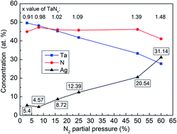
The temperature coefficient of resistance (TCR) of TaNx/Ag nanocomposite thin films could be substantially tuned by changing the components, even down to zero. In the work of this paper, it is unexpectedly found that the concentration of silver incorporation in the TaNx/Ag thin films could be controlled over a broad range from 5.4 at% to 31.14 at% through changing the N2 partial pressure during magnetron sputtering. In particular, the near-zero TCR of −15 ppm K−1 and the highest resistivity of 6038 μΩ cm were obtained in the TaNx/Ag thin films with 12.39 at% Ag. The high resistivity can be attributed to the low carrier density as a result of recombination of holes in the TaNx matrix and electrons in Ag. The composites changes from p-type to n-type at a higher Ag component. The results highlight a new approach to obtain high-performance thin films with zero TCR.
1. Introduction
With the rapid development of high-precision electrical circuits for use in harsh conditions, research on thin-film resistors with a near-zero temperature coefficient of resistance (TCR) is gradually increasing.1–3 In recent years, tantalum nitride (TaNx, 0 ≤ x ≤ 1.67 (ref. 4–6)) as an excellent candidate to fabricate high-performance film resistors with a near-zero TCR has attracted more and more attention.7–9 In particular, TaNx can be applied in embedded resistors due to the temperature insensitive resistivity, corrosion resistance and good chemical inertness.9–12 Na et al.7 and Riekkinen et al.13 demonstrated that Ta2N thin films exhibited a resistivity of 180–230 μΩ cm and a negative TCR value of −100–−287 ppm K−1. However, the resistivity and TCR of TaNx thin films were strongly dependent on the N2 partial pressure in magnetron sputtering.7 As the N2 partial pressure in magnetron sputtering is changed, several phases, such as, Ta2N, TaN in hexagonal or face centered cubic lattice, and Ta3N5, could be obtained. Therefore, it is still very challenging to fabricate near-stoichiometric Ta2N films.13 Furthermore, the aforementioned TCR at the magnitude order of −200 ppm K−1 can not meet the demands of high-precision electric circuits. To overcome this issue, TaNx/Cu and TaNx/Ag composite thin films with near-zero TCR were fabricated by using reactive co-sputtering. Essentially, the near-zero TCR is due to the balance between the negative TCR of TaNx and the positive TCR of metal.14–17 Technologically, the concentration of Ag in the thin films is usually controlled by varying the sputtering power on the Ag target. Unfortunately, Ag has a very high sputtering yield and extremely sensitive to the target power, it is difficult to accurately control the concentration of Ag incorporation by changing the target power.
Interestingly, it was found that Ta target could react with N2 in plasma, resulting in tantalum nitrides on the Ta target.18,19 In such a case, the sputtering of Ta will be suppressed, and the higher is the N2 partial pressure, the stronger is the effect. But the sputtering of Ag target is independent on the N2 partial pressure. As a result, the Ag component in the thin films increases with N2 partial pressure. The accuracy of a flow mass meter is usually 0.01 sccm, which is more accurate and manipulable than the power supply (usually 1 W). Hence, the Ag component in the compound thin films should be controlled more accurately by changing N2 partial pressure.
The sputtering magnetized method using two-phase nano-composite to control intrinsic properties in a composite form has been previously reported in other systems.20,21 Such as the remarkable enhanced low-field magnetoresistance (LFMR) properties in vertically aligned nano-composite thin films had been obtained by controlling the ratio of La0.7Sr0.3MnO3 and ZnO.22 The advanced control of crystallographic orientations and magnetic properties of self-assembled nano-structures via rational selections of substrates was also demonstrated in BiFeO3–CoFe2O4 system.23 In fact, many other two-phase nano-structured thin film systems had been developed to successfully tune the microstructure or achieve better physical properties.24–27
Based on the two-phase nano-structured thin film deposition technology, TaNx/Ag composite thin films were prepared on Si substrates by magnetron co-sputtering in this paper. The Ag component in the TaNx/Ag thin films was finely adjusted by changing the N2 partial pressure during sputtering. The composition, microstructures, and the electrical properties of the TaNx/Ag thin films were characterized comprehensively to explore the possibility of fabricate high-performance resistor thin films with near-zero TCR.
2. Experimental
TaNx/Ag composite thin films were prepared by using reactive co-sputtering of Ta and Ag targets (99.99% in purity) on n-type (100) orientated Si wafers covered with thermally grown SiO2 300 nm in thickness. Prior to deposition, the substrates were ultrasonically cleaned in acetone and ethanol. The deposition was done in the mixed gas of argon (99.999% purity) and nitrogen (99.999% purity) with a total pressure of 0.5 Pa at room temperature. A radio frequency (RF) power of 180 W with a frequency of 13.56 MHz was applied on the Ag target, while a direct-current (DC) power of 200 W was adopted on the Ta target. The mass flow-meters (D08-8C, Beijing Sevenstar Electronics) with a precision of 0.01 sccm were used to control the flow rates of Ar and N2 gas flow. The N2 partial pressure was changed from 3% to 60% in order to tune the concentration and microstructure in TaNx/Ag thin films. In addition, the targets were tilted by 30°, the target–target distance and the target-to-substrate distance were kept at 150 mm and 120 mm, respectively. The sputtering chamber was evacuated to a base pressure of 2 × 10⁻⁴ Pa before deposition and the deposition duration was conducted for 30 minutes.
The crystalline phases were analyzed by Grazing Incident Angle X-ray Diffractometer (GIXRD, XRD-7000) at an incident angle of 2° using Cu Kα radiation with a wavelength of 0.15418 nm. The composition of the thin films was determined using X-ray photoelectron spectroscopy (XPS) with monochromatic Al Kα X-ray and recorded by a VG ESCALABMK 250 spectrometer. In order to obtain reliable depth profile, the standard method of Ar+ ion sputtering was adopted to produce proper surface damage with the etching rate of appr. 6 nm min−1, and the etching voltage and etching current were chosen to be 2000 eV and 2 μA, respectively. In order to guarantee the proper depth profile measurement of deposited nano composite film, the sampled area with a size scale of 2 mm × 2 mm was larger than the detective spot diameter of XPS. The microstructure of the TaNx/Ag thin films was characterized by transmission electron microscopy (JEM-2100F). The resistivity and TCR were measured by a four-point probe system (RTS-9, 4PROBES TECH) attached with a precise hot stage. TCR values were calculated according to the following equation
| |
 | (1) |
in which
ρ120 and
ρ20 are the resistivities measured at 120 °C and 20 °C, respectively. The carrier density and Hall mobility of the thin films were evaluated by Hall effect measurement (Lakeshore 7707A Hall effect system) at room temperature. The Model 7704A Hall effect measurement system can determine sample Hall coefficient, Hall mobility, carrier concentration, and current–voltage characteristics. Real-time feedback of processed measurement data can be displayed in graphical and tabular format. The measurement basically consists of electromagnet, gaussmeter, matrix instrument, sample holder module and bipolar magnet power supply. As the sample is approximately two-dimensional, the measuring accuracy strongly depends on the sample shape. So the samples with the size of 10 mm × 10 mm were prepared for determining the carrier concentration and carrier mobility. The 4-contact van der pauw method was used to measure the Hall effect in current study.
3. Results and discussion
Fig. 1 shows the XRD patterns of the TaNx/Ag thin films deposited at different N2 partial pressures. As for the thin films deposited at 3% N2 partial pressure, only the (111) plane of TaN can be identified and no peaks of Ag is visible, indicating that Ag atoms are completely dissolved in nano-grained TaN matrix. As the N2 partial pressure is increased, the peak of Ag (111) plane appears and becomes sharper and higher, but the peaks of TaN become broader and lower, and eventually disappear. It means that TaN becomes amorphous gradually but Ag is crystallized. It was reported that introduction of a second element would disturb the lattice structure of crystals, and even lead to amorphization when the component of the second element is large enough.28,29 Therefore, the evolution of TaN phase from crystal to amorphous can be attributed to the change in Ag component with the increasing N2 partial pressure.
 |
| | Fig. 1 GIXRD patterns of the as-deposited TaNx/Ag thin films deposited with the N2 partial pressures: (I) 3%, (II) 8%, (III) 16%, (IV) 25%, (V) 60%. | |
Fig. 2 shows the XPS spectra of Ta 4f and Ag 3d in the thin films deposited at different N2 partial pressure. The binding energy is corrected referencing to C 1s peak at 284.6 eV. As shown in Fig. 2(a), two peaks at ∼367.8 and ∼373.8 eV corresponding to Ag 3d5/2 and Ag 3d3/2 states can be observed in all the thin films. According to the NIST X-ray Photoelectron Spectroscopy Database, the standard peaks of pure Ag 3d5/2 and Ag 3d3/2 are located at ∼368.2 and ∼374.2 eV, respectively. In contrast, there is a very little offset to higher binding energy of approximately 0.4 eV for Ag 3d3/2, indicating a slight degree of Ag nitridation in the composite film. Fig. 2(b) shows the evolution of the Ta 4f spectrum at different N2 partial pressures. In the thin film deposited at 3% N2 partial pressure, the XPS peaks appear at ∼22.8 and ∼24.7 eV respectively, which are less than the binding energy values in the Ta 4f spectrum of TaN (Ta 4f7/2 = 23.6–23.7 eV and Ta 4f5/2 = 25.5–25.7 eV) in literature.30–32 According to previous research results, the peaks of the pure metallic Ta0 are located at ∼21.7 and ∼23.6 eV, the peak positions will shift to higher binding energy side with the increasing of the N/Ta ratio of tantalum nitride,30,33 which is consistent with our results. Since it was very difficult to fabricate near-stoichiometric TaN film even in a narrow N2 partial pressure range, so TaNx thin film obtained in our study is usually a mixture of several phases.7,12,13 In addition, the unnoticeable Ta 4f5/2 peak located at ∼28 eV should be attributed to very little Ta2O5.
 |
| | Fig. 2 XPS spectra of the TaNx/Ag thin films: (a) Ag 3d and (b) Ta 4f. (I) 3%, (II) 8%, (III) 16%, (IV) 25%, (V) 60%. | |
Fig. 3 displays the elemental concentration in the thin films analyzed by XPS. Apparently, as the N2 partial pressure is increased, the Ag component increases substantially from 5.4 at% to 31.14 at%, but the concentrations of Ta and N decrease. It indicates the effectiveness of tuning Ag component by N2 partial pressure. The x value of TaNx matrix increases with the increasing of N2 partial pressure, which is in good agreement with the literatures.12,30 The different behaviors of Ta and Ag under N2 partial pressure have been studied comprehensively. Gladczuk et al.34 found that tantalum nitrides could usually be formed on the Ta target at higher nitrogen gas concentration, which would suppress the sputtering of Ta and lower the deposition rate of tantalum nitride. Chen et al.6 and Sellers et al.35 observed the similar results and they ascribed the lowered deposition rate to the formation of TaNx on Ta target and the well-known poisoning effect. Abendroth et al.36 addressed that a balance of nitrogen adsorption on surface, ion implantation and sputtering existed in the process. Some other investigations also demonstrated that the sputtering yield of Ta decreased when N2 was adopted as reactive gas because of the same physical process.18,19,37 As a result, the concentration of Ta and TaN in the thin films decreases but the concentration of Ag increases.
 |
| | Fig. 3 The components in the TaNx/Ag thin films. | |
In order to ensure the structural stability and reliable performance of TaNx/Ag thin films, it is very crucial to assess component homogenity of the deposited thin film along the depth profile at a given N2 partial pressures. Therefore, the TaNx/Ag thin film is investigated in depth profile by XPS, as shown in Fig. 4. It is shown that each component concentration of TaNx/Ag thin films deposited at 50% N2 partial pressure keeps in a constant level regardless of etching time indicating the homogeneous composition distribution of the deposited thin film along the depth profile. So it is not hard to deduce that the reaction of Ta target with N2 reaches a balance in a very short period of time at a given N2 partial pressures.
 |
| | Fig. 4 The component of the TaNx/Ag thin films deposited at 50% N2 partial pressure as a function of etching time of XPS. | |
Fig. 5 shows the cross-sectional bright-field TEM images of the TaNx/Ag thin films. As exhibited in Fig. 5(a), no crystalline phase of Ag can be identified in the thin films deposited at 3% N2 partial pressure, that is, Ag atoms are dispersed in the amorphous TaNx matrix, which confirms the supposition according to the XRD patterns. When the N2 partial pressure is in the range of 8–60%, the Ag component increases from 4.57 at% to 31.14 at%, and Ag nano-grains are homogeneously embedded in the amorphous TaNx matrix. In fact, the composite microstructure is crucial to obtain the near-zero TCR in TaNx/metal thin films.1,16 The separable metal nanoparticles, which have positive TCR and very low resistivity, could neutralize the negative TCR and reduce high resistivity of TaNx (x > 1). But, once mix metal nanoparticles contact each other, the resistivity of the deposited thin films will decrease sharply and the TCR will appear the metallic features.
 |
| | Fig. 5 Bright-field TEM images of the TaNx/Ag thin films deposited at different N2 partial pressure: (a) 3%, (b) 8%, (c) 25%, (d) 60%. | |
Fig. 6(a) and (b) shows the resistivity and TCR of the TaNx and TaNx/Ag thin films, respectively. As shown in Fig. 6(a), the resistivity of TaNx thin films increases with increasing N2 partial pressure, but the TCR decreases, which can be ascribed to the phase transformation from Ta2N and TaN to Ta3N5.7 As shown in Fig. 6(b), the resistivity of the TaNx/Ag composite thin films increases from 493 μΩ cm to 6038 μΩ cm when the N2 partial pressure is increased from 3% to 25%, and then the resistivity decreases with further increasing N2 partial pressure owing to the increased Ag component as addressed above. Previous reports7,16 obtained a resistivity of 180–230 μΩ cm and TCR value of −100–−287 ppm K−1 in the Ta2N thin films, a resistivity of 250–500 μΩ cm and TCR value of −600–−1500 ppm K−1 in TaN thin films, and a resistivity of >106 μΩ cm and TCR value of −2800–−7025 ppm K−1 in Ta3N5 thin films. Fig. 6(b) shows the evolution of resistivity and TCR in the TaNx/Ag thin films as a function of N2 partial pressure. During the first phase in which N2 partial pressure changes from 3% to 8%, the resistivity increases from 250–500 μΩ cm to 6038 μΩ cm and the TCR decreases from −272 ppm K−1 to −3465 ppm K−1. During the first phase, the change rules of resistivity and TCR of TaNx/Ag thin films are similar to those of the TaNx thin films [as shown in Fig. 6(a)], indicating that the phase of TaNx matrix dominates both the resistivity and TCR of TaNx/Ag composite thin films. During the second phase in which N2 partial pressure changes from 8% to 25%, the concentration of Ag in the TaNx/Ag thin films increases from 4.57 at% to 12.39 at%. As well known, Ag has positive TCR feature due to the Phonon scattering effect, which causes the increasing of the TCR of TaNx/Ag thin films. Meanwhile, the resistivity of TaNx/Ag thin films continues to rise due to the fact that the resistivity of TaNx matrix would increase with the increasing of the N2 partial pressure. During the third phase in which N2 partial pressure changes from 25% to 60%, the concentration of Ag in the TaNx/Ag thin films increases from 12.39 at% to 31.14 at%. The TaNx/Ag thin films gradually show metal properties with the increasing of the Ag concentration, so TaNx/Ag thin films exhibit lower resistivity and a more positive TCR characteristics. Especially, the near-zero TCR of −15 ppm K−1 and the highest resistivity of 6038 μΩ cm are obtained in the thin films deposited at 25% N2 partial pressure. The resistivity is higher than the best reported results and the TCR is more close to zero (TCR = +34 ppm K−1, resistivity = 5900 μΩ cm).16 The resistivity and TCR results of near-zero TCR thin film material in the recent literature are listed in Table 1.
 |
| | Fig. 6 Resistivity and TCR of thin films: (a) TaNx, (b) TaNx/Ag. | |
Table 1 Resistivity and TCR of thin film resistors
| Configuration of thin film layer |
Resistivity (μΩ cm) |
TCR (ppm K−1) |
Status |
| Ta2N40 |
234 |
−103 |
As-depo. |
| Ta/Ta3N5 (ref. 7) |
191 |
−284 |
As-depo. |
| Ta2N/RuO2 (ref. 41) |
651 |
−127 |
As-depo. |
| Ta2N/RuO2 (ref. 41) |
680 |
+126 |
Annealed |
| TaN/Cu14 |
1450 |
— |
Annealed |
| TaSiN/Ag1 |
542 |
+39.7 |
As-depo. |
| Ta3N5/Ag16 |
5900 |
+32 |
As-depo. |
As well known, the resistivity of material depends on the carrier concentration and carrier mobility.38 In general, the carrier mobility always reduces significantly at higher temperature due to the scattering effect stimulated by phonons, while the carrier concentration will increase due to increasing of the quantum tunneling effect between adjacent Ag nanoparticles. That is, the resistivity could be enhanced by phonon scattering as the temperature increases, while be weakened by quantum tunneling effect. Near-zero TCR is indeed a balance between these two effects.1
Fig. 7(a) shows the resistivity of TaNx and TaNx/Ag thin films for comparison. According to the resistivity-mixture rule,38 the effective resistivity of a multiphase mixture can be expressed as
where
Xα and
Xβ are the volume percentage of two phases, while
ρα and
ρβ are the resistivity of two phases, respectively. Therefore, if the matrix with higher resistivity is embedded with the phases with lower resistivity, the effective resistivity of the composites should be reduced. As shown in
Fig. 7(a), at the low N
2 partial pressure, the incorporation of Ag unexpectedly results in the increase of resistivity. In fact, the thin films with low Ag component are completely amorphous, as observed from the disordered atomic arrangement in the HR-TEM image in
Fig. 7(b) and the halo ring pattern in the selected area electron diffraction. Essentially, the motion of holes in semiconductor is the reverse movement of the electrons. As schematically displayed in
Fig. 8, the sparsely distributed Ag atoms in the TaN
x matrix act as the scattering centers, and thus prevent electrons from transporting. The mean free path of carriers will decrease and thus the drift mobility of carriers will decrease as well due to the impurity scattering. So the incorporation of a few Ag atoms will reduce the drift mobility of carriers and thus increase the resistivity. However, when a great number of Ag atoms are involved in TaN
x matrix and they become orderly arranged in local regions [
Fig. 7(b) to (d)], quantum tunneling effect and the aforementioned mixture rule works. This leads to lower resistivity in TaN
x/Ag composites as compared to TaN
x.
 |
| | Fig. 7 (a) The resistivity of TaNx and TaNx/Ag thin films, HR-TEM images and selected area electron diffraction patterns of the thin films deposited with different N2 partial pressure: (b) 3%, (c) 25%, (d) 60%. | |
 |
| | Fig. 8 Schematic mechanism for the scattering of electrons by Ag atoms and the recombination of the holes in TaNx matrix and the valence electrons from Ag atoms. | |
Fig. 9 shows the carrier concentration and the Hall carrier mobility. The electric conductivity of n-type semiconductors can be expressed as,39
in which
σ is the electrical conductivity,
n is the carrier concentration,
q is the electronic charge,
μ is the carrier mobility and
R is the resistivity. As shown in
Fig. 9, the product of carrier concentration and Hall mobility can well predict the variation tendency of conductivity. The thin films deposited at 25% N
2 partial pressure have the lowest carrier density of 6 × 10
16 per cm
3 and thus the highest resistivity. TaN
x matrix is a p-type semiconductor and the composites changes from p-type to n-type. It confirms the supposition that the high resistivity of 6038 μΩ cm obtained in TaN
x/Ag composites is due to the lowered carrier concentration as a result of recombination between the holes in TaN
x matrix and the valence electrons of Ag atoms (as shown in
Fig. 8).
 |
| | Fig. 9 The carrier density, Hall mobility of TaNx/Ag thin films and their product as a function of N2 partial pressure. | |
4. Conclusions
TaNx/Ag nano-composite thin films with near-zero TCR were prepared by reactive magnetron co-sputtering. The concentration of Ag in the TaNx/Ag thin films is changed in the range of 5.4–31.14 at% through changing the N2 partial pressure. In particular, the TaNx/Ag thin films of 12.39 at% Ag exhibit the near-zero TCR value of −15 ppm K−1 and the high resistivity of 6038 μΩ cm. The near-zero TCR is indeed a balance between quantum tunneling effect and phonon scattering effect. The high resistivity of 6038 μΩ cm obtained in TaNx/Ag composites is due to the lowered carrier concentration as a result of recombination between the holes in TaNx matrix and the valence electrons of Ag atoms. In the thin films with small Ag component, the sparsely distributed Ag atoms in the TaNx matrix act as the scattering centers, and thus prevent electrons from transporting. So the incorporation of a few Ag atoms will reduce the drift mobility of carriers and thus increase the resistivity. However, when a great number of Ag atoms are involved in TaNx matrix and they become orderly arranged in local regions, the resistivity in TaNx/Ag composites will be lowered. The TaNx/Ag nanocomposite thin films with a high resistivity and near-zero TCR can be adopted in low-power-consumption circuits.
Acknowledgements
This work was mainly supported by Key Project of Chinese National Programs for Fundamental Research and Development (Grant No. 2010CB631002), National Natural Science Foundation of China (Grant No. 51101081, 51271139 and 51471130). Natural Science Foundation of Shaanxi Province (2013JM6002), Fundamental Research Funds for the Central Universities.
References
- H. Gao, C. Li, F. Ma, Z. Song and K. Xu, J. Alloys Compd., 2015, 640, 147–153 CrossRef CAS.
- K. Chu and S.-H. Park, IEEE Electron Device Lett., 2015, 36, 50–52 CrossRef CAS.
- L. Ding, C. Wang, L. Chu, J. Yan, Y. Na, Q. Huang and X. Chen, Appl. Phys. Lett., 2011, 99, 251905 CrossRef.
- T.-C. Li, B.-J. Lwo, N.-W. Pu, S.-P. Yu and C.-H. Kao, Surf. Coat. Technol., 2006, 201, 1031–1036 CrossRef CAS.
- Y.-S. Wang, C.-C. Hung, W.-H. Lee, S.-C. Chang and Y.-L. Wang, Thin Solid Films, 2008, 516, 5241–5243 CrossRef CAS.
- Y.-I. Chen, B.-L. Lin, Y.-C. Kuo, J.-C. Huang, L.-C. Chang and Y.-T. Lin, Appl. Surf. Sci., 2011, 257, 6741–6749 CrossRef CAS.
- S.-M. Na, I.-S. Park, S.-Y. Park, G.-H. Jeong and S.-J. Suh, Thin Solid Films, 2008, 516, 5465–5469 CrossRef CAS.
- S. M. Kang, S. G. Yoon, S. J. Suh and D. H. Yoon, Thin Solid Films, 2008, 516, 3568–3571 CrossRef CAS.
- A. Mellberg, S. P. Nicols, N. Rorsman and H. Zirath, Electrochem. Solid-State Lett., 2004, 7, G261 CrossRef CAS.
- O. Seok and M.-W. Ha, Solid-State Electron., 2015, 105, 1–5 CrossRef CAS.
- C. Huey-Ru, C. Ying-Chung, C. Ting-Chang, C. Kuan-Chang, T. Tsung-Ming, C. Tian-Jian, S. Chih-Cheng, T. Yi-Ting, L. Chih-Yang and L. Hua-Ching, IEEE Electron Device Lett., 2015, 36, 271–273 CrossRef.
- C.-C. Chang, J. S. Jeng and J. S. Chen, Thin Solid Films, 2002, 413, 46–51 CrossRef CAS.
- T. Riekkinen, J. Molarius, T. Laurila, A. Nurmela, I. Suni and J. K. Kivilahti, Microelectron. Eng., 2002, 64, 289–297 CrossRef CAS.
- C. M. Wang, J. H. Hsieh, C. Li, Y. Fu and T. P. Chen, Surf. Coat. Technol., 2005, 193, 173–177 CrossRef CAS.
- C. M. Wang, J. H. Hsieh and C. Li, Thin Solid Films, 2004, 469–470, 455–459 CrossRef CAS.
- I.-S. Park, S.-Y. Park, G.-H. Jeong, S.-M. Na and S.-J. Suh, Thin Solid Films, 2008, 516, 5409–5413 CrossRef CAS.
- I.-S. Park, S.-H. Na, J.-S. Kim, S.-K. Lim, T.-S. Kim and S.-J. Suh, J. Korean Phys. Soc., 2009, 54, 2323–2326 CrossRef CAS.
- D. Depla and R. De Gryse, Surf. Coat. Technol., 2004, 183, 196–203 CrossRef CAS.
- D. Depla and R. De Gryse, Surf. Coat. Technol., 2004, 183, 190–195 CrossRef CAS.
- O. Chaix-Pluchery, C. Cochard, P. Jadhav, J. Kreisel, N. Dix, F. Sanchez and J. Fontcuberta, Appl. Phys. Lett., 2011, 99, 3 CrossRef.
- S. Park, Y. Horibe, T. Asada, L. S. Wielunski, N. Lee, P. L. Bonanno, S. M. O'Malley, A. A. Sirenko, A. Kazimirov, M. Tanimura, T. Gustafsson and S. W. Cheong, Nano Lett., 2008, 8, 720–724 CrossRef CAS PubMed.
- A. Chen, Z. Bi, C. F. Tsai, J. Lee, Q. Su, X. Zhang, Q. Jia, J. L. MacManus-Driscoll and H. Wang, Adv. Funct. Mater., 2011, 21, 2423–2429 CrossRef CAS.
- S.-C. Liao, P.-Y. Tsai, C.-W. Liang, H.-J. Liu, J.-C. Yang, S.-J. Lin, C.-H. Lai and Y.-H. Chu, ACS Nano, 2011, 5, 4118–4122 CrossRef CAS PubMed.
- Y. H. Hsieh, J. M. Liou, B. C. Huang, C. W. Liang, Q. He, Q. Zhan, Y. P. Chiu, Y. C. Chen and Y. H. Chu, Adv. Mater., 2012, 24, 4564–4568 CrossRef CAS PubMed.
- A. Chen, Z. Bi, Q. Jia, J. L. MacManus-Driscoll and H. Wang, Acta Mater., 2013, 61, 2783–2792 CrossRef CAS.
- N. Dix, R. Muralidharan, J.-M. Rebled, S. Estradé, F. Peiró, M. Varela, J. Fontcuberta and F. Sánchez, ACS Nano, 2010, 4, 4955–4961 CrossRef CAS PubMed.
- J. Yoon, S. Cho, J. H. Kim, J. Lee, Z. Bi, A. Serquis, X. Zhang, A. Manthiram and H. Wang, Adv. Funct. Mater., 2009, 19, 3868–3873 CrossRef CAS.
- Y. Meng, Z. X. Song, D. Qian, W. J. Dai, J. F. Wang, F. Ma, Y. H. Li and K. W. Xu, J. Alloys Compd., 2014, 588, 461–464 CrossRef CAS.
- K.-Y. Mun, T. E. Hong, T. Cheon, Y. Jang, B.-Y. Lim, S. Kim and S.-H. Kim, Thin Solid Films, 2014, 562, 118–125 CrossRef CAS.
- A. Arranz and C. Palacio, Appl. Phys. A: Mater. Sci. Process., 2005, 81, 1405–1410 CrossRef CAS.
- L. Li, E. Niu, G. Lv, X. Zhang, H. Chen, S. Fan, C. Liu and S.-Z. Yang, Appl. Surf. Sci., 2007, 253, 6811–6816 CrossRef CAS.
- X. Liu, G. J. Ma, G. Sun, Y. P. Duan and S. H. Liu, Appl. Surf. Sci., 2011, 258, 1033–1037 CrossRef CAS.
- S. Badrinarayanan and S. Sinha, J. Appl. Phys., 1991, 69, 1141–1146 CrossRef CAS.
- L. Gladczuk, A. Patel, J. D. Demaree and M. Sosnowski, Thin Solid Films, 2005, 476, 295–302 CrossRef CAS.
- J. Sellers, Surf. Coat. Technol., 1998, 98, 1245–1250 CrossRef CAS.
- D. Güttler, B. Abendroth, R. Grötzschel, W. Möller and D. Depla, Appl. Phys. Lett., 2004, 85, 6134–6136 CrossRef.
- D. Depla and R. De Gryse, Surf. Coat. Technol., 2004, 183, 196–203 CrossRef CAS.
- S. O. Kasap, Principles of electronic materials and devices, McGraw-Hill, 2006 Search PubMed.
- E. Liu, B. Zhu and J. Luo, Physics of semiconductors, Pulishing House Of Electronics Industry, 7th edn, 2008 Search PubMed.
- T. Riekkinen, J. Molarius, T. Laurila, A. Nurmela, I. Suni and J. Kivilahti, Microelectron. Eng., 2002, 64, 289–297 CrossRef CAS.
- E. Ma and W. Anderson, Mater. Sci. Eng., B, 1997, 47, 161–166 CrossRef.
|
| This journal is © The Royal Society of Chemistry 2016 |
Click here to see how this site uses Cookies. View our privacy policy here.