
Structural, electronic, optical, vibrational and transport properties of CuBX2 (X = S, Se, Te) chalcopyrites
S. Bagcia,
Battal G. Yalcin*a,
H. A. Rahnamaye Aliabadb,
S. Dumana and
B. Salmankurta
aDepartment of Physics, Sakarya University, Esentepe Campus, 54187 Sakarya, Turkey. E-mail: gyalcin@sakarya.edu.tr; Fax: +90 264 295 5950; Tel: +90 264 295 6094
bDepartment of Physics, Hakim Sabzevari University, Sabzevar, Iran
First published on 7th June 2016
Abstract
The structural, electronic and optical properties of CuBX2 (X = S, Se, Te) chalcopyrite semiconductors have been studied using the full-potential (linearized) augmented plane-wave (FP(L)APW) method based on the density functional theory (DFT) within the Yukawa screened-PBE0 (YS-PBE0) hybrid functional as implemented in the WIEN2k package. We have found that our calculated structural and electronic parameters such as lattice parameter, tetragonal ratio, anion displacement and energy band gap are in very good agreement with previous experimental results. We have also presented the real and imaginary parts of the dielectric function, refractive index and absorption coefficients to describe optical properties of the investigated chalcopyrite semiconductors. Furthermore, the phonon dispersion curves and corresponding density of states have been studied by using a linear response approach based on the density functional perturbation theory implemented in the Quantum ESPRESSO code. Finally, transport properties such as the Seebeck coefficient, thermal and electrical conductivity and the figure of merit for these materials have been calculated using the semi-classical Boltzmann theory as implemented in the BoltzTraP code.
1. Introduction
Ternary chalcopyrite semiconductors with the formula AIBIIICVI2 have been widely studied both theoretically and experimentally, because of their potential in technological applications, during the last few decades. These materials are used in electro-optical and optoelectronic devices such as photovoltaic optical detectors and light-emitting diodes or in non-linear optics.1–4 They are also promising candidates for use in solar cell devices and thermoelectric applications.5–10 Among them, Cu-based I–III–VI2 compounds have been the most widely studied in recent years,11–15 because of the incredible progress in the conversion efficiencies of solar cells based on CuInS2 (CIS) and CuInGaSe2 (CIGS).16–18 However, members of the CuBX2 (X = S, Se, Te) family of compounds have been investigated in few experimental and theoretical works. CuBS2 and CuBSe2 have been synthesized by two different groups, who have measured their structural parameters and electronic band gap energies.19,20 In these studies, the optimum values of the direct band gaps of CuBS2 and CuBSe2 were found to be 3.61 eV and 3.13 eV, respectively. In contrast to most I–III–VI2 compounds, the band gap values of CuBS2 and CuBSe2 fall in the UV region and these materials can be good candidates for use in UV photodetectors, UV light emitters and electronic power applications. It has also been found that there are few experimental studies of alloys, especially related to CuInBSe2, in the literature.21–23 On the other hand, the structural lattice parameters and electronic band gap energies of CuBX2 chalcopyrite materials have been calculated theoretically using informatics-based approaches.11,24 The electronic structures of CuBS2 and CuBSe2 have also been presented in terms of the density functional theory.25,26Although some progress has been made with the structural and electronic properties of CuBX2 chalcopyrite compounds, their optical, vibrational and thermoelectric properties are still not established. It is well known that the investigation of these properties will be very useful for the better understanding of the areas of technological application of these materials.
In this work, we have studied the structural and electronic properties of CuBS2, CuBSe2 and CuBTe2 chalcopyrite semiconductors using the full-potential (linearized) augmented plane-wave method (FP(L)APW) based on the generalized gradient approximation (GGA) of the density functional theory (DFT). We have also used the Yukawa screened-PBE0 (YS-PBE0) hybrid functional to obtain more accurate results for structural and electronic parameters, because it is clearly known that hybrid calculations have predicted more accurate results for the band gaps and other properties of chalcopyrite semiconductors.27–30 The optical properties such as the real and imaginary parts of the dielectric function, refractive index and absorption coefficients are also presented using a hybrid DFT method. The phonon dispersion curves and corresponding phonon density of states for the studied chalcopyrite semiconductors are presented and discussed in detail. The phonon calculations have been used to determine the dynamical stability of the studied compounds. CuBS2 and CuBSe2 are wide-band-gap semiconductors, which may also be good candidates for electronic power applications. Also, power devices based on wide-band-gap semiconductors can operate at high temperatures. Therefore, the Debye temperatures of CuBS2, CuBSe2 and CuBTe2 have also been calculated using phonon dispersion curves. At the end of this work, we have calculated the thermoelectric properties of the investigated ternary semiconductors using the BoltzTraP code31 implemented with the semi-classical Boltzmann theory. Our obtained results are compared with those previously reported for I–III–VI2 chalcopyrite semiconductors.
2. Computational details
Full-potential (linearized) augmented plane-wave (FP(L)APW) calculations were performed using the WIEN2k code32 in order to calculate the structural, electronic and optical properties of the studied compounds.It is a very important problem with calculations of self-consistent band structure within the density functional theory (DFT)33,34 that both the local density approximation (LDA)35 and the generalized gradient approximation (GGA)36 usually underestimate the band gap because the Kohn–Sham states do not take the quasiparticle self-energy into account correctly. Typically, the standard semi-local approximations (LDA or GGA) significantly underestimate the band gaps of semiconductors (∼30–100%).37,38 Thus, we have used the Yukawa screened-PBE0 (YS-PBE0)39 hybrid functional to obtain more accurate values of the band gap taking into account the exchange and correlation effects self-consistently. Hybrid functionals are usually more accurate than semi-local functionals for determining the electronic properties of semiconductors and insulators. In a hybrid functional, the α fraction of semi-local (SL) exchange is replaced by Hartree–Fock (HF) exchange:
| Ehybridxc = EGGAxc + αx(EHFx − EGGAx) | (1) |
To obtain the total energy convergence, an energy cut-off parameter RMTKmax was defined as Kmax = 7.5/RminMT. The cut-off energy was set to −6 Ry. Self-consistent calculations were considered to be converged when the difference in energy between succeeding iterations was less than 10−4 Ry. We optimized the atomic positions of the ternary semiconductor CuBX2 (structural relaxation) by minimizing the forces (1 mRy per bohr) acting on the atoms. The self-consistent calculations were considered to be converged when the integral of the absolute charge density difference between the input and output electron densities was less than 0.0001|e| per formula unit, where e is the charge of an electron. The standard special k-points technique of Monkhorst and Pack (MP)40 was used for accurate integration of the Brillouin zone. The sizes of the k-meshes were a 6 × 6 × 6 MP k-mesh (28 special k-points) for the standard semi-local GGA calculations and a 4 × 4 × 4 k-mesh (13 special k-points in the irreducible wedge of the BZ) for the hybrid YS-PBE0 calculations. Also, the screening parameter (λ) was set at the YS-PBE0 value of 0.165 bohr−1 for all the investigated chalcopyrites. The k-meshes and basis sets were chosen to be good enough to obtain well-converged calculations.
The vibrational properties were calculated by using the Quantum ESPRESSO code,41 which is an implementation of the plane-wave pseudopotential approach within the framework of the density functional theory. It has been realized in the GGA using the Perdew–Burke–Ernzerhof method (GGA-PBE).36 To describe the electron–ion interactions, we used ultrasoft pseudopotentials.42 The electronic wavefunctions and charge density were expanded with kinetic energy cut-offs of 60 Ry and 240 Ry, respectively. The dynamical matrices were computed using a 4 × 4 × 4 q-point mesh and a Fourier interpolation was used to calculate the phonon frequencies for any chosen q-points. The obtained phonon frequencies were accurate to within 1 cm−1 for the present choice of the kinetic energy cut-off and the special k-points.
On the other hand, one of the most slowly converging processes with respect to k-point sampling in the Brillouin zone is the calculation of the optical properties of semiconducting materials. Therefore, the calculated optical properties such as the real and imaginary dielectric functions, absorption coefficient, etc., were converged with respect to k-point sampling. In this study, we used a fine k-mesh, namely a 21 × 21 × 21 k-mesh (726 k-points in the irreducible BZ), in order to obtain more accurate convergence. It is also well known that the standard PBE calculations usually underestimate the band gap of semiconductors. We aimed to obtain the frequency-dependent dielectric function. However, there is a high dependence on the value of the band gap with the dielectric function. To overcome this problem, the “scissors” approximation was employed, which consists of a shift of all the conduction bands by a gap correction. The scissor operator was set to 1.3, 1.25 and 0.75 eV for CuBS2, CuBSe2 and CuBTe2 chalcopyrite semiconductors, respectively.
In the current study, the thermoelectric properties were obtained from the calculated electronic structure using the BoltzTraP program,31 which is based on a well-tested smoothed Fourier interpolation to obtain an analytical expression of the bands.43,44 For the transport coefficients, we used a fine k-mesh, namely a 46 × 46 × 46 k-mesh (6780 k-points in the irreducible BZ), in order to obtain more accurate convergence. The relaxation time τ was assumed to be a constant with respect to the wave vector k and the energy around the Fermi level and the effect of doping were introduced by the rigid band approximation. The lpfac parameter, which represents the number of k-points per lattice point, was kept equal to 5 during the calculations of the transport coefficients.
3. Results and discussion
3.1. Structural and electronic properties
Before we present our obtained results, we have outlined the structures of the studied chalcopyrite compounds CuBX2 (X = S, Se and Te), which are derived from II–VI semiconductor materials. The space group (SG) of the chalcopyrite structure is I![[4 with combining macron]](https://www.rsc.org/images/entities/char_0034_0304.gif) 2m (point group: D122d; SG no: 122). These materials crystallize in a body-centered tetragonal Bravais lattice that has eight atoms per unit cell (Fig. 1). The Cu and B atoms are located at the Wyckoff positions 4a (0, 0, 0) and 4b (0, 0, 0.5), respectively, while the X atoms occupy the Wyckoff position 8d (x, 0.25, 0.125).
2m (point group: D122d; SG no: 122). These materials crystallize in a body-centered tetragonal Bravais lattice that has eight atoms per unit cell (Fig. 1). The Cu and B atoms are located at the Wyckoff positions 4a (0, 0, 0) and 4b (0, 0, 0.5), respectively, while the X atoms occupy the Wyckoff position 8d (x, 0.25, 0.125).
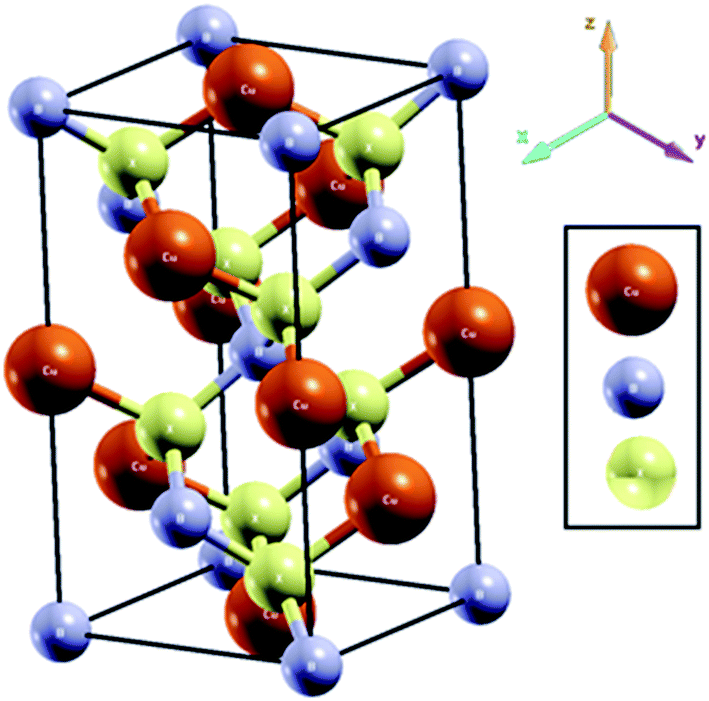 | ||
| Fig. 1 Crystal structure of CuBX2 chalcopyrite compound. Cu is located at (0, 0, 0), B at (0, 0, 0.5) and X (X = S, Se and Te) at (x, 0.25, 0.125). | ||
We first present the calculated total binding energy versus the cell volume for the studied ternary chalcopyrite semiconductors under both the hybrid YS-PBE0 and the semi-local PBE approximations in Fig. 2. We obtained a solid line by means of the Murnaghan equation of state45 in Fig. 2. The calculated structural properties (lattice parameter (a0), tetragonal ratio (η = c/2a) and anion displacement (u)) of the investigated ternary chalcopyrite semiconductor CuBX2 are summarized in Table 1 together with other theoretical24,26 and experimental19,20 data.
 | ||
| Fig. 2 Calculated total binding energy versus cell volume for CuBX2 compounds. | ||
| Material | CuBS2 | CuBSe2 | CuBTe2 |
|---|---|---|---|
| Lattice parameter a0 (Å) | 5.003 (PBE) | 5.165 (PBE) | 5.526 (PBE) |
| 4.976 (PBE) | 5.252 (YS-PBE0) | 5.616 (YS-PBE0) | |
| 5.0643 (YS-PBE0) | 5.782 (ref. 20) exp | 5.133 (ref. 24) | |
| 5.044 (ref. 19) exp | 4.956 (ref. 24) | ||
| 5.337 (ref. 26) PBE | |||
| Tetragonal ratio (η = c/2a) | 0.908 (PBE) | 0.961 (PBE) | 0.929 (PBE) |
| 0.898 (YS-PBE0) | 0.955 (YS-PBE0) | 0.948 (YS-PBE0) | |
| 0.887 (ref. 19) exp | 0.986 (ref. 20) exp | ||
| 0.911 (ref. 26) PBE | |||
| Anion displacement (u) | 0.197 (PBE) | 0.207 (PBE) | 0.216 (PBE) |
| 0.305 (YS-PBE0) | 0.294 (YS-PBE0) | 0.285 (YS-PBE0) | |
| 0.308 (ref. 19) exp | 0.202 (ref. 26) PBE | ||
| Eg (eV) | 1.568 (PBE) | 1.520 (PBE) | 1.138 (PBE) |
| 3.622 (YS-PBE0) | 3.180 (hybrid) | 2.558 (hybrid) | |
| 3.610 (ref. 19) exp | 1.960 (ref. 24) theory | 2.850 (ref. 24) | |
| 3.440 (ref. 25) mBJ | 3.130 (ref. 20) exp | ||
| 1.506 (ref. 26) PBE |
The calculated crystal constants such as a0, η = c/2a, and u have formerly been demonstrated to improve within hybrid functionals as compared with standard semi-local approximations.39,46–48 Therefore, only the hybrid YS-PBE0 structural results are discussed here. One can clearly see from the table that the calculated values of a0 show good agreement with experimental19,20 and theoretical24,26 works. The calculated tetragonal ratio (η) of CuBS2 (0.898) is 1.24% larger than the experimental value of 0.887.19 The tetragonal ratio of CuBSe2 (0.955) is underestimated by about 3.24% compared with the experimental value of 0.986.20 The calculated tetragonal ratio (η) shows a small deviation from the reported values for the chalcopyrite phase (c/2a = 1.0).49 The value of the anion displacement (u) of 0.305 for CuBS2 agrees very well with the experimental value of 0.308.19
On the other hand, we have also calculated the bulk moduli of these structures by means of the Murnaghan equation of states. The calculated bulk moduli were found to be 120.13, 99.35 and 86.97 GPa, respectively, for CuBS2, CuBSe2 and CuBTe2. With reference to our results, the calculated bulk modulus of these materials decreases from CuBS2 to CuBTe2, i.e., from lower to higher atomic number, which indicates that CuBS2 has the lowest compressibility whereas CuBTe2 has the highest compressibility. The decreasing trend in the calculated bulk modulus agrees well with the literature.13,15
In this study, the electronic band structure of the investigated materials was obtained self-consistently by using their equilibrium lattice parameters along the high-symmetry directions in the Brillouin zone (BZ). We present the electronic band structures of the CuBX2 compounds using the PBE and hybrid YS-PBE0 schemes in Fig. 3. The Fermi level is shifted to zero and is shown by the horizontal dashed lines in Fig. 3. It should also be noted that the valence band maximum and conduction band minimum are located at the Γ point, as the investigated compounds display direct-band-gap semiconductor character at the Γ point, as shown in Fig. 3.
 | ||
| Fig. 3 Electronic band structures of (a) CuBS2, (b) CuBSe2 and (c) CuBTe2. The solid (red) lines indicate results obtained using YS-PBE0, whereas the PBE results are shown by dashed (black) lines. | ||
It can be seen that, compared with the results of the semi-local potential PBE, the hybrid YS-PBE0 results tend to shift slightly to higher valence states. The calculated band gap values obtained with PBE and the hybrid YS-PBE0 are presented in Table 1 together with former theoretical24–26 and experimental values.19,20 The calculated band gap values with (YS-PBE0; PBE) are (3.622; 1.568 eV), (3.180; 1.520 eV) and (2.558; 1.138 eV) for CuBS2, CuBSe2 and CuBTe2, respectively. The obtained results under (YS-PBE0; PBE) calculations are underestimated by (0.33%; 56%) and (1.6%; 52%) compared with the experimental band gap values of 3.61 eV (ref. 19) and 3.13 eV (ref. 20) for CuBS2 and CuBSe2, respectively. The calculated PBE results display a large deviation from the experimental data as a result of the fact that self-interaction error and the absence of derivative discontinuity in the exchange–correlation potential can cause an underestimation of the energy band gap.50,51 It is also clearly seen from a comparison with the experimental work19 that our reported band gap value for CuBS2 under the hybrid YS-PBE0 calculation is more accurate than that from the theoretical work using the mBJ scheme.25 To the best of our knowledge, there is no experimental report of the electronic properties of CuBTe2. On the other hand, the calculated band gap value of CuBTe2 under the hybrid YS-PBE0 calculation is underestimated by 10% compared with the theoretically predicted value of 2.85 eV.24 The inconsistency between these studies essentially arises from the calculation methods employed.
A knowledge of the electronic density of states (DOS) is required to understand and clarify some properties of materials such as their band structures, bonding character, dielectric function, etc. In order to have a deeper understanding of these properties of the studied compounds, the total and partial DOS have also been calculated. The total and partial densities of states (DOS) for the investigated structures are shown in Fig. 4. We have only shown the hybrid YS-PBE0 results in Fig. 4 to avoid confusion between PBE and hybrid YS-PBE0. The Fermi level is arbitrarily shifted to the origin. It is clearly seen from this figure that the valence bands are dominated by 3d states of Cu in all cases. There is a small contribution of B 2p states to the valence bands compared with S 3p, Se 4p or Te 5p states, whereas the conduction band originates principally from B 2p states.
 | ||
| Fig. 4 Calculated total and partial density of states for (a) CuBS2, (b) CuBSe2 and (c) CuBTe2 using the hybrid YS-PBE0 scheme. The Fermi level is indicated by the vertical line at zero energy. | ||
3.2. Optical properties
The investigation of the optical properties of CuBX2 (X = S, Se, Te) chalcopyrite semiconductors is very important, because they are potentially good candidates for optoelectronic applications. It is well known that the main optical parameters of solids are related to their complex dielectric function, ε(ω) = ε1(ω) + iε2(ω), where ε1(ω) is the real part and ε2(ω) is the imaginary part of the dielectric function. The real and imaginary parts of the dielectric function have been calculated using the following equations:52,53
 | (2) |
 | (3) |
Fig. 5 shows the real parts of the dielectric functions obtained by GGA (PBE) and hybrid (YS-PBE0) calculations for CuBX2 (X = S, Se, Te) chalcopyrite semiconductors. It is clearly seen from this figure that the static dielectric function ε1(0) increases from CuBS2 to CuBTe2, as expected, whereas the energy band gap decreases for both calculations. This inverse feature could be associated with Penn's model: ε1(0) ≈ 1 + (ħωp/Eg)2,54 where ωp and Eg are the plasma frequency and the energy band gap, respectively. We present the ε1(0) values in Table 2 and the ε1(0) values calculated by the PBE functional are higher than the results for the hybrid functional. The main peaks in ε1(ω) obtained by GGA calculations are situated at 2.92, 2.26 and 2.18 eV for CuBS2, CuBSe2 and CuBTe2, respectively, which are located in the visible region of the spectrum. On the other hand, the main peaks calculated by the hybrid functional are found at 5.54, 3.60 and 3.46 eV for CuBS2, CuBSe2 and CuBTe2 semiconductors, respectively. These energy values are located in the ultraviolet region. The difference in energy between the GGA and hybrid calculations is related to the different nature of these functionals. There are some regions where the real part of the dielectric function has a negative value in Fig. 5 for both calculation methods, and these values show that incident photons are totally reflected in these regions.
 | ||
| Fig. 5 The real parts of the dielectric functions obtained by GGA (PBE) and hybrid (YS-PBE0) calculations for CuBX2 (X = S, Se, Te) semiconductors. | ||
| Method | ε1(0) | ε1xx(0) | ε1zz(0) | n(0) | nxx(0) | nzz(0) | |
|---|---|---|---|---|---|---|---|
| CuBS2 | YS-PBE0 | 2.28 | 2.25 | 2.35 | 1.51 | 1.50 | 1.54 |
| PBE | 8.86 | 9.02 | 8.54 | 2.98 | 3.00 | 2.92 | |
| CuBSe2 | YS-PBE0 | 2.86 | 2.67 | 3.23 | 1.69 | 1.64 | 1.80 |
| PBE | 10.51 | 10.32 | 10.90 | 3.24 | 3.22 | 3.30 | |
| CuBTe2 | YS-PBE0 | 3.22 | 3.08 | 3.50 | 1.79 | 1.75 | 1.87 |
| PBE | 11.43 | 11.36 | 11.56 | 3.38 | 3.37 | 3.41 |
The imaginary parts of the dielectric functions for CuBX2 semiconductors are presented in Fig. 6. Although there are shifts in energy in the locations of the peaks obtained by GGA and hybrid calculations, the general patterns of the curves are similar to each other. The fundamental absorption limit has been found to be 3.49 (1.40), 2.90 (1.28) and 2.35 (1.02) eV using GGA results with (without) the scissor operator and 3.49, 2.90 and 2.35 eV using hybrid calculations for CuBS2, CuBSe2 and CuBTe2, respectively. For the results of the hybrid functional, the main peaks for CuBSe2 and CuBTe2 are located between energy values of 3.5 and 5 eV, whereas they are calculated to lie between 4.5 and 6.5 eV for CuBS2. It is clearly seen from Fig. 4 that these peaks can originate from a transition from the Cu 3d states just below the Fermi level to the B 2p states above the Fermi level.
 | ||
| Fig. 6 The imaginary parts of the dielectric functions obtained by GGA (PBE) and hybrid (YS-PBE0) calculations for CuBX2 (X = S, Se, Te) semiconductors. | ||
Another important optical constant is the absorption coefficient α(ω), which is a measure of the amount of light absorbed by a given medium. The absorption coefficients for CuBS2, CuBSe2 and CuBTe2 are presented in Fig. 7. This figure shows that the general patterns of the curves obtained by GGA calculations have a similar character to the results for the hybrid functional. The highest absorption peaks for all three compounds occur in the ultraviolet region. It is well known that these peaks are produced from inter-band transitions between various high-symmetry points in the electronic band spectrum. The results for the hybrid functional in Fig. 7 show that the main peaks in αzz are higher than the results for αxx for all three semiconductors, which means that absorption along the z (E ∥ c) axis is greater than along the x or y (E ⊥ c) axes. It should also be noted that these compounds may be good absorbers in the low and medium UV regions, as indicated in Fig. 7.
 | ||
| Fig. 7 The absorption coefficients obtained by GGA (PBE) and hybrid (YS-PBE0) calculations for CuBX2 (X = S, Se, Te) semiconductors. | ||
The refractive index n(ω) plays an important role with respect to the electronic and optical properties of materials. The calculated values of the refractive index using the GGA and hybrid functionals for CuBX2 (X = S, Se, Te) semiconductors are presented in Fig. 8. We found that the curves obtained using the GGA and hybrid functionals have a similar pattern to each other. The sharp peaks in the refractive index spectrum result from excitonic transitions at the energy band gap edge. For the results of the hybrid functional, the highest refractive index was found around 4 eV, which is located in the ultraviolet region. The static refractive indices n(0) obtained from Fig. 8 are presented in Table 2. These results are found to be 1.51, 1.69 and 1.79 for CuBS2, CuBSe2 and CuBTe2, respectively. These results show that n(0) increases from CuBS2 to CuBTe2. This increase has also been found for CuAlX2, CuGaX2 and CuInX2 while X changes from S to Te.15
 | ||
| Fig. 8 The refractive indices obtained by GGA (PBE) and hybrid (YS-PBE0) calculations for CuBX2 (X = S, Se, Te) semiconductors. | ||
3.3. Vibrational properties
The calculated phonon dispersion curves of CuBS2, CuBSe2 and CuBTe2 are shown in Fig. 9. It can be seen from this figure that all the phonon modes are positive, which indicates that these materials are dynamically stable in the chalcopyrite structure. There are 24 vibrational phonon modes in the phonon spectra, which is due to the fact that the chalcopyrite structure has eight atoms in its body-centered tetragonal primitive unit cell (see Fig. 1). All the phonon modes can be seen along the Γ–X and Γ–N symmetry directions, separately. However, we have observed 14 and 12 phonon branches along the Γ–Z and X–P high-symmetry directions, respectively. The character table of ternary chalcopyrite (point group symmetry D2d) includes five different types of irreducible representation, A1, A2, B1, B2 and E. At the Γ point, group theory predicts that the following phonon modes are:55| Γac = B2 + E | (4) |
| Γopt = A1 + 2A2 + 3B1 + 3B2 + 6E | (5) |
 | ||
| Fig. 9 The calculated phonon dispersion curves for CuBS2 (a), CuBSe2 (b) and CuBTe2 (c). | ||
All the optical phonon modes are Raman-active except A2. Raman-active phonon modes require the existence of a finite change in polarizability during the phonon vibration. The A2 phonon modes include only vibrations of cationic atoms; the eigenvalues of anionic atoms are zero. However, only the B2 and E phonon branches are infrared (IR)-active. The A1 and B1 phonon modes are not IR-active but are Raman-active, because they do not have a dipole moment due to the fact that these include the out-of-phase motion of all ions in the unit cell. In spite of the long-range polarization interactions, the IR-active phonon modes are split into TO and LO components. Three B2 modes exhibit polarization along the c axis, whereas six E modes exhibit polarization along the x or y directions. The B2 modes have a dipole moment, because each cation pair vibrates in in-phase motion and two anion pairs in out-of-phase motion along the principal axis. However, the E phonon modes are twofold-degenerate and a dipole moment occurs in the xy plane, because each cation pair vibrates only along the x or y directions. It is clearly known that E and B2 phonon modes exhibit angular dependence. As can be seen from the phonon dispersion figure, these phonon modes are not continuous along the X–Γ–Z directions at the center of the Brillouin zone, because of the anisotropic nature of the tetragonal structure of these chalcopyrite materials.
The calculated zone-center phonon frequencies of CuBS2, CuBSe2 and CuBTe2 are given in Table 3. The obtained results are compared between each other without any previous theoretical or experimental data. It can be seen from the table that the overall frequencies of phonons decrease with an increase in the mass of the anionic atoms. The highest optical phonon mode (E1(LO)) is mainly formed from the vibrations of cation (B)–anion (S, Se or Te) bonds. This phonon mode is related to the force constants of cation (B)–anion (S, Se or Te) bonds. The calculated bond lengths of B–S, B–Se and B–Te are found to be 1.93, 2.08 and 2.29 Å, respectively. Because the smallest distance occurs for B–S, the highest optical phonon frequency of CuBS2 is expected to have a higher frequency compared with the others, as can be seen in Fig. 9. However, this phonon mode of CuBTe2 exhibits less dispersion than its counterparts for the other compounds.
| Mode | CuBS2 | CuBSe2 | CuBTe2 | |
|---|---|---|---|---|
| Γ1 | A1 | 377.524 | 222.886 | 162.994 |
| Γ2 | A12 | 429.849 | 247.959 | 178.932 |
| A22 | 359.900 | 216.912 | 161.841 | |
| Γ3 | B11 | 636.040 | 580.106 | 526.558 |
| B21 | 387.112 | 244.657 | 198.486 | |
| B31 | 132.789 | 116.533 | 110.334 | |
| Γ4 | B12(TO) | 579.771 | 501.672 | 478.289 |
| B22(TO) | 357.832 | 235.183 | 201.884 | |
| B32(TO) | 178.803 | 135.167 | 113.825 | |
| B12(LO) | 619.750 | 523.157 | 481.877 | |
| B22(LO) | 360.120 | 235.848 | 202.095 | |
| B32(LO) | 178.872 | 135.169 | 113.838 | |
| Γ5 | E1(TO) | 660.856 | 586.795 | 535.723 |
| E1(LO) | 686.354 | 600.025 | 538.349 | |
| E2(TO) | 595.888 | 528.305 | 490.420 | |
| E2(LO) | 598.245 | 529.983 | 490.427 | |
| E3(TO) | 342.992 | 229.248 | 208.677 | |
| E3(LO) | 343.093 | 229.821 | 209.110 | |
| E4(TO) | 321.621 | 218.673 | 192.548 | |
| E4(LO) | 322.139 | 218.834 | 192.742 | |
| E5(TO) | 217.131 | 164.776 | 123.343 | |
| E5(LO) | 218.149 | 166.108 | 123.489 | |
| E6(TO) | 107.951 | 79.039 | 70.954 | |
| E6(LO) | 108.050 | 79.140 | 70.959 | |
The calculated total and partial phonon densities of states for these semiconductors are shown in Fig. 10. It can be seen from this figure that CuBS2 and CuBSe2 have two forbidden gaps, whereas CuBTe2 has one forbidden optical gap. The forbidden phonon energy gap increases with the increasing difference in mass between cationic and anionic atoms. It is clear that the main contribution to the high optical frequency region is supplied by the B atoms, whereas the Cu atoms are more dominant than the other atoms in the acoustical frequency region for all semiconductors.
 | ||
| Fig. 10 The calculated total and partial density of states for CuBS2 (a), CuBSe2 (b) and CuBTe2 (c). | ||
The Debye temperatures of CuBS2, CuBSe2 and CuBTe2 were also calculated using phonon dispersion curves. The calculated Debye temperatures were found to be 664 K, 508 K and 438 K for CuBS2, CuBSe2 and CuBTe2, respectively. From these results, it should be noted that CuBS2 and CuBSe2 can operate in electronic power devices at high temperatures due to their wide band gaps.
3.4. Transport properties
The figure of merit or performance of a thermoelectric compound is defined by ZT = S2σT/κ, where S is the Seebeck coefficient, σ is the electrical conductivity and κ represents the thermal conductivity. For excellent thermometric materials, ZT is about equal to or larger than unity.56 For the calculation of ZT, we first investigate the Seebeck coefficient, then the thermal and electrical conductivities are discussed. Finally, calculated values of ZT are given.The temperature gradient between two different materials creates a potential difference in the Seebeck effect. Free electrons move from the higher-temperature location towards the lower-temperature location. The Seebeck coefficient (S.C) is defined in units of volts per kelvin.57 The variation in the S.C with respect to the chemical potential (μ) for CuBX2 (X = S, Se, Te) compounds at 300 (room temperature), 400, 600, 800 and 1000 K are shown in Fig. 11. The values of μ0 are 7.61, 6.69 and 6.93 eV for CuBS2, CuBSe2 and CuBTe2, respectively. The results show that the highest values of the Seebeck coefficient for the studied structures are achieved at room temperature. For p-type CuBX2 (X = S, Se, Te) compounds, the Seebeck coefficients have maximum values of 2295 μV K−1 (at 300 K), 2527 μV K−1 (at 300 K) and 1704 μV K−1 (at 300 K) respectively, which shows that these compounds are good candidates for thermoelectric materials. The calculated Seebeck coefficients of these semiconductors around 400 K are approximately five times higher than those of CuGaTe2 (ref. 58) and CuInTe2.59 Fig. 11(a) shows that the curve of the S.C increases with temperature at 300 K for CuBS2, then decreases almost exponentially with temperature. On the other hand, it decreases almost exponentially with temperature for n- and p-type CuBSe2 and CuBTe2 materials, which is in agreement with the thermoelectric character of p-type doped AgGaTe2.60 The conduction of heat in a material or thermal conductivity originates from electronic and lattice contributions.61 In the present calculations, the electronic part of thermal conductivity, κel, is determined under the assumption that it is independent of the relaxation time τ, which is given as κel/τ. Good thermoelectric materials have low thermal conductivity. Fig. 12 presents the thermal conductivities of CuBX2 (X = S, Se, Te) compounds at 300 (room temperature), 400, 600, 800 and 1000 K. The thermal conductivity at room temperature remains approximately zero between chemical potentials of (−0.12, −0.57, −0.30) eV and (0.17, 0.55, 0.33) eV for CuBX2 (X = S, Se, Te) compounds, respectively. In this region, these compounds have maximum efficiency. Fig. 12(a) shows that the thermal conductivity decreases with temperature at 400 K for CuBS2, then increases with temperature. This property increases with temperature for n- and p-type CuBSe2 and CuBTe2.
 | ||
| Fig. 11 The Seebeck coefficients of (a) CuBS2, (b) CuBSe2 and (c) CuBTe2 as a function of the chemical potential at 300, 400, 600, 800 and 1000 K. | ||
 | ||
| Fig. 12 The electronic thermal conductivities of (a) CuBS2, (b) CuBSe2 and (c) CuBTe2 as a function of the chemical potential at 300, 400, 600, 800 and 1000 K. | ||
Electrical conductivity is defined by the flow of free electrons in a compound. The movement of electrons from high-temperature regions to low-temperature regions is electric current.62 Good thermoelectric materials have high electrical conductivity. The electrical conductivities of CuBX2 (X = S, Se, Te) compounds are displayed in Fig. 13. Fig. 13(a) shows that the electrical conductivity decreases with temperature from 300 K to given temperatures for CuBS2, then remains the same at other temperatures. Besides, in Fig. 13(b) and (c) this property is constant with temperature for n- and p-type CuBSe2 and CuBTe2.
 | ||
| Fig. 13 The electrical conductivities of (a) CuBS2, (b) CuBSe2 and (c) CuBTe2 as a function of the chemical potential at 300, 400, 600, 800 and 1000 K. | ||
Fig. 14(a)–(c) display the figure of merit ZT for CuBX2 (X = S, Se, Te) compounds. Fig. 14(a) shows that at room temperature ZT for CuBS2 is larger than unity (1.02 for p-type and 1.04 for n-type). ZT rises sharply from zero and the peak value is obtained at chemical potentials of −0.12 and 0.30 eV for CuBS2. For the other compounds, it is very close to unity. Therefore, these compounds can be used in thermoelectric devices. On the other hand, the obtained maximum value of ZT of the studied structures is higher than that of p-type AgGaTe2,9 which has displayed a ZT value of 0.8 with partial optimization. However, these compounds exhibit lower ZT values compared with other Cu-based chalcopyrites such as CuGaTe2 (ref. 58) and CuInTe2.63 These results show that ZT decreases with temperature for all materials, both n- and p-types.
 | ||
| Fig. 14 The figure of merit (ZT) for (a) CuBS2, (b) CuBSe2 and (c) CuBTe2 as a function of the chemical potential at 300, 400, 600, 800 and 1000 K. | ||
4. Conclusions
In this study, we first calculated the structural parameters such as the lattice constant, tetragonal ratio, anion displacement parameter, and electronic energy band gap for CuBS2, CuBSe2 and CuBTe2 chalcopyrite semiconductors using both GGA and YS-PBE0 functionals based on the density functional theory. We found that our results using the hybrid functional are better than results using GGA, according to previous corresponding experimental results. The energy band gap has been calculated to be 3.622 eV for CuBS2 and 3.180 eV for CuBSe2 using YS-PBE0. These results are in very good agreement with corresponding experimental results of 3.610 and 3.130 eV, whereas our results using GGA are 1.568 and 1.520 eV for CuBS2 and CuBSe2, respectively.The optical properties of CuBS2, CuBSe2 and CuBTe2 have also been presented. The general pattern of optical parameters such as the real and imaginary parts of the dielectric function, absorption coefficient and refractive index has a similar character for both polarizations, namely, xx (E ⊥ c-axis) and zz (E ∥ c-axis), although there are some small differences in energy between them. The static dielectric function ε1(0) and refractive index n(0) increase from CuBS2 to CuBTe2. We have also found that the band gaps of CuBS2 and CuBSe2 fall in the UV range and these materials can be good candidates for use in UV photodetectors, UV light emitters and electronic power applications owing to their fundamental absorption limits and the fact that they exhibit the highest absorption peaks.
Furthermore, the phonon dispersion curves and the total and partial densities of phonon states for the studied chalcopyrite structures have been calculated using the density functional perturbation theory and a linear response approach. Analysis of the phonon spectra shows that CuBS2, CuBSe2 and CuBTe2 are dynamically stable in the tetragonal structure. The calculated Debye temperatures are found to be 664 K, 508 K and 438 K for CuBS2, CuBSe2 and CuBTe2, respectively. From these results, it should be noted that CuBS2 and CuBSe2 can be employed in electronic power devices at high temperatures due to their wide band gaps.
Finally, the Seebeck coefficient, electronic thermal conductivity, electrical conductivity and figure of merit have been calculated to describe the transport properties of CuBS2, CuBSe2 and CuBTe2. The calculated Seebeck coefficients of these semiconductors around 400 K are approximately five times higher than those of CuGaTe2 and CuInTe2. The obtained maximum ZT value of the studied structures is higher than that of p-type AgGaTe2, which has displayed a ZT value of 0.8 with partial optimization. However, these compounds exhibit a lower ZT value compared with other Cu-based chalcopyrites such as CuGaTe2 and CuInTe2. Using these results related to transport properties, these chalcopyrite semiconductors can be used in thermoelectric devices.
References
- A. S. Verma, Philos. Mag., 2009, 89, 183 CrossRef CAS.
- G. C. Catella and D. Burlage, Mater. Res. Soc. Bull., 1998, 23, 28 CrossRef CAS.
- A. Zunger and J. E. Jaffe, Phys. Rev. Lett., 1983, 51, 662 CrossRef CAS.
- W. R. L. Lambrecht and S. N. Rashkeev, J. Phys. Chem. Solids, 2003, 64, 1615 CrossRef CAS.
- L. L. Kazmerski, Nuovo Cimento Soc. Ital. Fis., D, 1983, 2, 2013 CrossRef.
- S. Mishra and B. Ganguli, Solid State Commun., 2011, 151, 523–528 CrossRef CAS.
- S. Mishra and B. Ganguli, J. Alloys Compd., 2012, 512, 17–22 CrossRef CAS.
- S. Mishra and B. Ganguli, J. Solid State Chem., 2015, 232, 131–137 CrossRef CAS.
- D. Parker and D. J. Singh, Phys. Rev. B: Condens. Matter Mater. Phys., 2012, 85, 125209 CrossRef.
- A. H. Reshak, J. Phys. Chem. Solids, 2015, 78, 46 CrossRef CAS.
- P. Dey, J. Bible, S. Datta, S. Broderick, J. Jasinski, M. Sunkara, M. Menon and K. Rajan, Comput. Mater. Sci., 2014, 83, 185 CrossRef CAS.
- A. Shabaev, M. J. Mehl and A. L. Efros, Phys. Rev. B: Condens. Matter Mater. Phys., 2015, 92, 035431 CrossRef.
- M. G. Brik, J. Phys.: Condens. Matter, 2009, 21, 485502 CrossRef CAS PubMed.
- J. Kaneshiro, N. Gaillard, R. Rocheleau and E. Miller, Sol. Energy Mater. Sol. Cells, 2010, 94, 12 CrossRef CAS.
- A. Ghosh, R. Thangavel and M. Rajagopalan, J. Mater. Sci., 2015, 50, 1710 CrossRef CAS.
- D. C. Peng, J. W. Chen and C. J. Wu, Sol. Energy Mater. Sol. Cells, 2011, 95, 257 CrossRef.
- I. Repins, M. A. Contreras, B. Egaas, C. DeHart, J. Scharf, C. L. Perkins, B. To and R. Noufi, Prog. Photovoltaics, 2008, 16, 235 CAS.
- P. Jackson, D. Hariskos, E. Lotter, S. Paetel, R. Wuerz, R. Menner, W. Wischmann and M. Powalla, Prog. Photovoltaics, 2011, 19, 894 CAS.
- T. Kajiki, Y. Hayashi and H. Takizawa, Mater. Lett., 2007, 61, 2382 CrossRef CAS.
- L.-J. Chen, J.-D. Liao and Y.-J. Chuang, CrystEngComm, 2011, 13, 2909 RSC.
- N. J. Ianno, R. J. Soukup, T. Santero, C. Kamler, J. H. Love, S. A. Darveau, J. Olejnicek and C. L Exstrom, Mater. Res. Soc. Symp. Proc., 2007, 1012, Y03–Y21 CrossRef.
- L.-J. Chen, J.-D. Liao, Y.-J. Chuang and Y.-S. Fu, J. Am. Chem. Soc., 2011, 133, 3704 CrossRef CAS PubMed.
- C. A. Kamler, R. J. Soukup, N. J. Ianno, J. L. Huguenin-Love, J. Olejníček, S. A. Darveau and C. L. Exstrom, Sol. Energy Mater. Sol. Cells, 2009, 93, 45 CrossRef CAS.
- Y. Zheng, S. J. Chua and P. Wu, Chem. Mater., 2002, 14, 2989 CrossRef.
- Y. M. Basalaev, A. B. Gordienko and S. I. Filippov, Phys. Solid State, 2012, 54, 1764 CrossRef CAS.
- Y. Cheng, K. Wei, P. Xia and Q. Bai, RSC Adv., 2015, 5, 85431 RSC.
- J. Pohl and K. Albe, J. Appl. Phys., 2010, 108, 023509 CrossRef.
- J. Vidal, S. Botti, P. Olsson, J.-F. Guillemoles and L. Reining, Phys. Rev. Lett., 2010, 104, 056401 CrossRef PubMed.
- C. L. Bailey, L. Liborio, G. Mallia, S. Tomic and N. M. Harrison, Phys. Rev. B: Condens. Matter Mater. Phys., 2010, 81, 205214 CrossRef.
- G. M. D. Nguimdo and D. P. Joubert, Eur. Phys. J. B, 2015, 88, 113 CrossRef.
- K. Georg, H. Madsen and D. J. Singh, Comput. Phys. Commun., 2006, 175, 67 CrossRef.
- P. Blaha, K. Schwarz, G. K. H. Madsen, D. Kvasnicka and J. Luitz, WIEN2K: An Augmented Plane Wave Plus Local Orbitals Program for Calculating Crystal Properties, ed. K. Schwarz, Vienna University of Technology, Austria, 2001 Search PubMed.
- P. Hohenberg and W. Kohn, Phys. Rev., 1964, 136, B864–B871 CrossRef.
- W. Kohn and L. J. Sham, Phys. Rev., 1965, 140, A1133–A1138 CrossRef.
- J. P. Perdew and Y. Wang, Phys. Rev. B: Condens. Matter Mater. Phys., 1992, 45, 13244–13249 CrossRef.
- J. P. Perdew, K. Burke and M. Ernzerhof, Phys. Rev. Lett., 1996, 77, 3865–3868 CrossRef CAS PubMed.
- C. S. Wang and W. E. Pickett, Phys. Rev. Lett., 1983, 51, 597 CrossRef CAS.
- R. O. Jones and O. Gunnarsson, Rev. Mod. Phys., 1989, 61, 689 CrossRef CAS.
- F. Tran and P. Blaha, Phys. Rev. B: Condens. Matter Mater. Phys., 2011, 83, 235118 CrossRef.
- H. J. Monkhorst and J. D. Park, Phys. Rev. B: Condens. Matter Mater. Phys., 1976, 13, 5188–5192 CrossRef.
- P. Giannozzi, S. Baroni, N. Bonini, M. Calandra, R. Car, C. Cavazzoni, D. Ceresoli, G. L. Chiarotti, M. Cococcioni, I. Dabo, A. Dal Corso, S. de Gironcoli, S. Fabris, G. Fratesi, R. Gebauer, U. Gerstmann, C. Gougoussis, A. Kokalj, M. Lazzeri, L. Martin-Samos, N. Marzari, F. Mauri, R. Mazzarello, S. Paolini, A. Pasquarello, L. Paulatto, C. Sbraccia, S. Scandolo, G. Sclauzero, A. P. Seitsonen, A. Smogunov, P. Umari and R. M. Wentzcovitch, J. Phys.: Condens. Matter, 2009, 21, 395502 CrossRef PubMed.
- K. F. Garrity, J. W. Bennett, K. M. Rabe and D. Vanderbilt, Comput. Mater. Sci., 2014, 81, 446–452 CrossRef CAS.
- G. K. H. Madsen and D. J. Singh, Comput. Phys. Commun., 2006, 175, 67 CrossRef CAS.
- T. J. Scheidemantel, C. Ambrosch-Draxl, T. Thonhauser, J. V. Badding and J. O. Sofo, Phys. Rev. B: Condens. Matter Mater. Phys., 2003, 68, 125210 CrossRef.
- F. D. Murnaghan, Proc. Natl. Acad. Sci. U. S. A., 1944, 30, 244 CrossRef CAS.
- H. Xiao, J. Tahir-Kheli and W. A. Goddard, J. Phys. Chem. Lett., 2011, 2, 212–217 CrossRef CAS.
- J. L. F. Da Silva, M. V. Ganduglia-Pirovano, J. Sauer, V. Bayer and G. Kresse, Phys. Rev. B: Condens. Matter Mater. Phys., 2007, 75, 045121 CrossRef.
- Y. Kumagai, M. Choi, Y. Nose and F. Oba, Phys. Rev. B: Condens. Matter Mater. Phys., 2014, 90, 125202 CrossRef.
- B. J. Stanbery, Crit. Rev. Solid State Mater. Sci., 2002, 27, 73 CrossRef CAS.
- R. W. Godby, M. Schlüter and L. J. Sham, Phys. Rev. Lett., 1986, 56, 2415 CrossRef CAS PubMed.
- M. Stadele, J. A. Majewski, P. Vogl and A. Gorling, Phys. Rev. Lett., 1997, 79, 2089 CrossRef.
- R. de and L. Kronig, On The Theory Of Dispersion Of X-Rays, J. Opt. Soc. Am., 1926, 12, 547–556 CrossRef.
- H. A. Kramers, Atti Cong. Intern. Fisica, 1927, 2, 545–557 Search PubMed.
- D. R. Penn, Phys. Rev. B: Condens. Matter Mater. Phys., 1962, 128, 2093 CAS.
- G. D. Holah, J. S. Webb and H. Montgomery, J. Phys. C: Solid State Phys., 1974, 7, 3875 CrossRef CAS.
- H. A. Rahnamaye Aliabad, M. Ghazanfari, I. Ahmad and M. A. Saeed, Comput. Mater. Sci., 2012, 65, 509–519 CrossRef CAS.
- M. Bilal, B. Khan, H. A. Rahnamaye Aliabad, M. Maqbool, S. Jalali Asadabadi and I. Ahmad, Comput. Phys. Commun., 2014, 185, 1394–1398 CrossRef CAS.
- T. Plirdpring, K. Kurosaki, A. Kosuga, T. Day, S. Firdosy, V. Ravi, G. J. Snyder, A. Harnwunggmoung, T. Sugahara, Y. Ohishi, H. Muta and S. Yamanaka, Adv. Mater., 2012, 24, 3622 CrossRef CAS PubMed.
- V. Kucek, C. Drasar, J. Navratil, T. Plechacek and L. Benes, J. Phys. Chem. Solids, 2015, 83, 18–23 CrossRef CAS.
- W. Wu, K. Wu, Z. Ma and R. Sa, Chem. Phys. Lett., 2012, 537, 62–64 CrossRef CAS.
- H. A. Rahnamaye Aliabad and Z. Parvizi, Comput. Mater. Sci., 2014, 93, 125–132 CrossRef CAS.
- H. A. Rahnamaye Aliabad and M. Kheirabadi, Phys. B, 2014, 433, 157–164 CrossRef CAS.
- R. Liu, L. Xi, H. Liu, X. Shi, W. Zhang and L. Chen, Chem. Commun., 2012, 48, 3818–3820 RSC.
| This journal is © The Royal Society of Chemistry 2016 |