
Wavelength dependent nonlinear optical switching in electron beam irradiated CuTTBPc thin film
K. V. Anil Kumar*a,
S. Venugopal Raob,
S. Hamadb and
S. M. Dharmaprakasha
aDepartment of Studies in Physics, Mangalore University, Karnataka 574199, India. E-mail: anilkumarkv86@gmail.com
bAdvanced Centre of Research in High Energy Materials (ACRHEM), University of Hyderabad, Telangana 500046, India
First published on 18th February 2016
Abstract
The main aim of the present work is to investigate the role of 8 MeV electron beam interaction in modifying the linear and nonlinear optical (NLO) properties of thermally evaporated copper tetra tert-butyl phthalocyanine (CuTTBPc) thin films. The irradiation dose dependent change in linear optical band gap and roughness changes after electron irradiation have been explored. Third order NLO investigations were performed for unirradiated and 10 kGy irradiated CuTTBPc films with the femtosecond (fs) Z-scan technique at wavelengths of 800 nm and 900 nm. The unirradiated film depicted both reverse saturable and saturable kinds of nonlinear absorption behaviour as expected from the band gap restrictions on two photon absorption. A switch over to reverse saturable absorption within saturable absorption of the irradiated film at 900 nm laser excitation is explained using the irradiation induced band gap shifts of the material due to localized defects formation within the band gap region.
1. Introduction
The interaction of various radiations, such as electron, gamma, proton etc. with matter has been a subject of intensive research over past few decades.1–3 Such interactions can bring overwhelming and indispensable changes in the physical properties of the material depending the characteristics of both the interacting radiation and the material.4 Knowledge of aforesaid radiation sensitive materials is imperative, especially when they are intended for device applications or forming an integral part of devices to avoid the reflecting nature of changed parameters on device properties and characteristics during the time of operation under extreme radiation conditions such as high radiation environment of nuclear plants, extra-terrestrial (i.e. space) applications etc. The emerging realm of technology encourages organic material for its futuristic device fabrication strategies due to large number of physical property tailoring options avail with the organics through easy structural modifications during the design through molecular engineering.5 Phthalocyanines (Pc) belongs to such a class of extensively studied semiconductor organic compounds for its versatility in multidisciplinary areas like gas sensing, organic thin film transistor, solar cell, photodynamic therapy, nonlinear optics etc.6–8Phthalocyanine compounds are one of the well explored organic nonlinear optical (NLO) materials for its inherent third order optical nonlinearities. The π-electrons in the macromolecule are free to move throughout the system, making their axially/peripherally substituted derivatives potential candidate for NLO applications by extending the π-electron delocalization of the conjugated system. Metal inclusion in phthalocyanine macrocycles creates energy sublevels in the complex, allowing electronic transitions to take place and also changes molecular electron density through metal–ligand charge transfer mechanism, thus improving the NLO performance of the complex.9 Phthalocyanine compounds with higher reverse saturable absorption (RSA) type nonlinear absorption (NLA) coefficients are promising candidates for optical limiting while; with suitable nonlinear refractions (NLR) coefficients are advantageous in fast optical switching applications.10 Many of Pc based NLO studies performed on solution/doped in polymer matrix pose a hindrance in understanding the device applicability of the material because of the distinctive and different characteristic behaviour in solution and solid state.11–13 Thus far, the third order NLO properties of thermally evaporated, solid state Pc's remain less explored.9,14 Even after optimizing NLO parameters, irradiation opens a huge opportunity to further modify the material properties.4,15
RSA is a leading NLA mechanism of third order optical nonlinearity in most of the dyes, especially with Pc. The switchover from saturable absorption (SA) to RSA or vice versa has been observed by many researchers in different materials including Pc. Most of such reported shifting was connected with changed laser intensity, concentration of materials (in solution), pulse width or exited state lifetime, etc.16,17 Recently reversible protonation induced NLA switching were reported for pyrazine derivatives.18 Intensity dependent NLA favours SA for lower laser intensity and RSA shifting is associated with higher threshold intensity based on materials.19 Wavelength dependent shift of the NLA mechanisms are also reported.10,20,21 The NLA switching characteristics of the material makes them attractive towards design of optical switches and logic gates for realizing all optical information processing.22 In the present work, the impact of 8 MeV electron beam irradiation on NLO properties of thermally evaporated phthalocyanine thin films have been studied at two different wavelengths for the first time. NLA mechanism in unirradiated and electron beam irradiated CuTTBPc thin film is discussed within the frame work of two photon absorption (TPA) requirement of phthalocyanine semiconductor materials. In addition, SA to RSA switching behaviour of electron irradiated film at 900 nm is correlated with the band gap shifts resulted due to irradiation induced localized states within the band gap region. The NLO coefficients are extracted from the theoretical fits to the obtained experimental data.
2. Materials and methods
2.1 Thin film deposition
Copper(II) tetra tert-butyl phthalocyanine (CuTTBPc) powder (Sigma-Aldrich) was used as the source material for thin film preparation. Molecular structure of the CuTTBPc molecule is shown in Fig. 1. The sample powder was taken in a molybdenum boat and is kept inside the bell jar. We used ultrasonically cleaned glass plates of dimension 37 × 12 × 1 mm as the substrate for film deposition and is arranged vertically above (∼15 cm) the sample holding boat. The bell jar kept the sample isolated from the surrounding and thin film deposition carried out once the vacuum was created to the required level using the ‘Hind Hi-Vac’ instrument, operating with thermal evaporation technique. CuTTBPc films were coated under a pressure range of 10−5 Torr and rate of deposition was controlled to ∼2 nm s−1. | ||
| Fig. 1 Molecular structure of CuTTBPc investigated in the present study. | ||
2.2 Basic measurements and devices used
As deposited CuTTBPc films were annealed at 473 K for 90 minutes inside a high temperature muffle furnace and forms ACuTTBPc films. The accuracy of thin film thickness recorded using thickness monitoring attachment (quartz crystal) of the coating unit is later verified through ellipsometry and is found to be ∼200 nm. The electron beam irradiation of selected ACuTTBPc films carried out with the aid of an electron accelerator (Microtron, Mangalore University) having an output energy of 8 MeV to deliver a dose of 1, 2, 5 and 10 kGy and results in irradiated ACuTTBPc (AECuTTBPc) films. UV-vis absorption study of the ACuTTBPc and AECuTTBPc films conducted using Shimadzu-1800 UV-vis spectrophotometer. Thin film surface morphology and root mean square (RMS) roughness of ACuTTBPc and AECuTTBPc films were analysed with the help of Agilent 5500 AFM operated in non-contact mode. ACuTTBPc and 10 kGy electron irradiated AECuTTBPc films were selected for performing nonlinear optical studies with femtosecond (fs) pulses. Fs pulses were generated by separate Ti: sapphire laser (Chameleon, Coherent) operating at a repetition rate of 80 MHz delivering ∼140 fs pulses which were tunable in the 680–1060 nm wavelength region. The input beam was spatially filtered to achieve a pure Gaussian profile in the far field. Z-scan studies were performed by focusing the 2 mm diameter input beam using a 100 mm focal length convex lens. The sample was placed on a 10 μm resolution translation stage and the detector (Thermal Sensor-Field Max, Coherent) was used to collect data manually.3. Results and discussion
3.1 Linear absorption spectra and dose dependent nature of band gap
UV-visible absorption spectra of CuTTBPc and ACuTTBPc molecules presented in the Fig. 2. Inset of the Fig. 2 is the absorption spectra of 1, 2, 5 and 10 kGy electron irradiated AECuTTBPc films. CuTTBPc film has a shoulder positioned in the 660–690 nm spectral range apart from the main peak at 624 nm. This shoulder is the characteristic of thermally evaporated CuTTBPc as a result of Davydov splitting. Absorption peaks in the spectra of Pc molecules originates from the π–π* transition in Q band.23 | ||
| Fig. 2 UV-vis absorption spectra of CuTTBPc and ACuTTBPc films. The inset shows absorption spectra of AECuTTBPc for different doses. | ||
There exists a strong coupling between the phthalocyanine ligand and the central metal ion in metal phthalocyanine molecules. In comparison with CuPc literature, as deposited film is identified as the unstable polymorphic phase of CuTTBPc and after annealing at 473 K the stable phase is formed.24 ACuTTBPc is characterized with a suppressed shoulder as observed in Fig. 2. In particular, no significant change in the band edge region has been observed after annealing at 473 K. Induced changes due to different doses of electron beam irradiation found to affect specially on the band edge or band gap tailoring region (inset of Fig. 2). Thus band gap calculations were made using the relation
| α0 = B(hν − Eg)r |
From the above relation, linear absorption coefficient ‘α0’ (= 2.303![[thin space (1/6-em)]](https://www.rsc.org/images/entities/char_2009.gif) logA/d) can be calculated by knowing absorbance (A) and film thickness (d). B is a constant which depends on the transition probability, Eg is the band gap and ‘r’ value is 1/2. From the absorption characteristics of CuTTBPc, we calculated the direct band gap of the material and the value is obtained from the energy axis (inset of Fig. 3) by extrapolating the linear portion of the α02 versus the incident photon energy (hν) graph. We observed a shift in the optical band gap of AECuTTBPc film up on electron irradiation with different doses and band gap found to change inversely with irradiation dose (Fig. 3). Structural studies carried out with powder XRD (not reported here) shows no change in peak positions of AECuTTBPc but a slight variation in intensity, imparting information regarding compositional stability and unaltered lattice constants of the material after electron beam irradiation. This implies the possible reason for the observed band gap changes might be associated with the small defects or disorders caused by electron irradiation. Reduced crystallinity and grain size of AECuTTBPc film may be the indicative of the fragmentation caused by the strain developed during irradiation and thereby grain boundary gets changed.25 Increased absorbance in the visible region (i.e. 380–550 nm) is directly proportional to the electron irradiation doses and the region become asymmetric compared to that of CuTTBPc and ACuTTBPc film. The observed changes may be emanating from the band edge shifts upon irradiation.
logA/d) can be calculated by knowing absorbance (A) and film thickness (d). B is a constant which depends on the transition probability, Eg is the band gap and ‘r’ value is 1/2. From the absorption characteristics of CuTTBPc, we calculated the direct band gap of the material and the value is obtained from the energy axis (inset of Fig. 3) by extrapolating the linear portion of the α02 versus the incident photon energy (hν) graph. We observed a shift in the optical band gap of AECuTTBPc film up on electron irradiation with different doses and band gap found to change inversely with irradiation dose (Fig. 3). Structural studies carried out with powder XRD (not reported here) shows no change in peak positions of AECuTTBPc but a slight variation in intensity, imparting information regarding compositional stability and unaltered lattice constants of the material after electron beam irradiation. This implies the possible reason for the observed band gap changes might be associated with the small defects or disorders caused by electron irradiation. Reduced crystallinity and grain size of AECuTTBPc film may be the indicative of the fragmentation caused by the strain developed during irradiation and thereby grain boundary gets changed.25 Increased absorbance in the visible region (i.e. 380–550 nm) is directly proportional to the electron irradiation doses and the region become asymmetric compared to that of CuTTBPc and ACuTTBPc film. The observed changes may be emanating from the band edge shifts upon irradiation.
 | ||
| Fig. 3 Variation in the band gap observed with different electron irradiation doses. | ||
3.2 Influence of electron beam irradiation on film morphology and roughness parameter
Morphological investigations of ACuTTBPc and AECuTTBPc films were performed with the noncontact mode AFM. The AFM image reveals the uniform morphologies of each film (ACuTTBPc and AECuTTBPc) as evident from Fig. 4 and 5. Small and granular shaped structures observed in the images. Up on electron beam irradiation, morphology of ACuTTBPc film changed slightly and formation of small crack has been observed. Small changes manifested in the AECuTTBPc film uniformity could be the implications of induced disorder and this may have changed the grain boundary. In the AFM image of AECuTTBPc one can observe enhanced grain size while comparing with ACuTTBPc film surface morphology. The observed discrepancies with the larger size of AECuTTBPc grains may be due to the coalesced particles of ACuTTBPc after irradiation.26 The RMS surface roughness of ACuTTBPc and AECuTTBPc films are 18.6 nm and 26.8 nm respectively. The results clearly indicate an increase in RMS roughness value of 8 MeV electron beam irradiated film and the observed changes may the result of surface modification due to electron irradiation.27 | ||
| Fig. 4 AFM image of ACuTTBPc thin film. | ||
 | ||
| Fig. 5 AFM image of AECuTTBPc thin film. | ||
The increased roughness of AECuTTBPc arises from electron irradiation created disorders and as a consequence, minor modifications manifests in the material. This leads to band edge change in AECuTTBPc film. Interestingly, these observations are in good agreement with the changes noticed in the band edge regions of UV-visible absorption studies.
3.3 Effect of electron irradiation on femtosecond NLO properties
Fs open aperture (OA) and closed aperture (CA) Z-scans were performed on ACuTTBPc as well as 10 kGy electron irradiated film (AECuTTBPc) with both 800 nm and 900 nm excitations to understand the effects of electron irradiation on the NLO properties of the film at these wavelengths. The experimental setup of Z-scan is pictorially represented below (Fig. 6). | ||
| Fig. 6 Schematic of the Z-scan experimental setup. | ||
Laser pulses generated by the oscillator were spatially filtered and an appropriate input energy selected with neutral density filters. The pulses focussed on to the sample film using 10 cm focal length lens as shown in Fig. 6. The sample film translated in +z and −z directions of the focussed Gaussian beam and the intensity change in output beam was detected with a power sensor. The linear transmittance of ACuTTBPc and AECuTTBPc films listed in Table 1 at both probing wavelengths. The reduced linear transmittance of AECuTTBPc is the consequence of electron irradiation. In CA, the laser beam is made to enter through a small aperture before the beam reaches the power sensor. The aperture and the lower energy of the CA scan minimizes the effects of NLA on NLR of Pc films. Prior to the sample film studies, substrate glass plates were tested and verified its NLO inactive nature at the wavelengths and energies used in the present study.
| Sl. no | Sample name | λ (nm) | Linear transmittance (%) | NLA coeff. (×10−4 cm W−1) | NLA | n2 (×10−8 cm2 W−1) |
|---|---|---|---|---|---|---|
| 1 | ACuTTBPc | 800 | 66 | 4.4 | RSA | 0.7 |
| 900 | 55 | −3.8 | SA | 0.8 | ||
| 2 | AECuTTBPc | 800 | 50 | 3.8 | RSA | 4 |
| 900 | 45 | 2.9 | SA in RSA | 1.8 |
Fig. 7(a)–(d) depict the results of OA Z-scan. The exact knowledge about the underlying NLA mechanism is very essential to extract the NLA coefficients. The laser propagation through the thin nonlinear sample medium with a total nonlinear absorption coefficient α(I) having a propagation distance of z′ and optical intensity I, is governed by the differential equation,  . NLA in presence of RSA is explained using the expression α(I) = α0 + βI. ‘β’ in the relation represents the NLA coefficient due to RSA and for SA, the first term takes the form, α0 = α0/(1 + I/Isat), where Isat is the saturation intensity. Thus, nonlinear absorption in presence of SA and RSA is given by the relation28

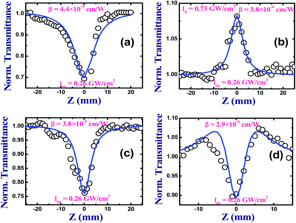 | ||
| Fig. 7 OA Z-scan results of ACuTTBPc at (a) 800 nm (b) 900 nm and AECuTTBPc at (c) 800 nm and (d) 900 nm. | ||
For pure RSA type NLA, Isat will be zero while pure SA does not hold RSA coefficient. The first and second term of the above relation respectively represents the negative and positive NLA. NLA coefficients can be extracted by fitting the experimental Z-scan data to theoretical relation given below,29

 , Rayleigh range (= πwo2/λ).
Since the present NLO study employs ultrashort pulses as well as the studied material is an organic moeity (phthalocyanine), we expect RSA type NLA in all our measurements.11,30 With fs laser pulses the RSA of Pc films could be of TPA origin. OA scan data with 800 nm wavelength shows a good theoretical fit with the TPA equation for both the ACuTTBPc and AECuTTBPc films. The study with 900 nm shows an interplay in NLA mechanism i.e., SA (ACuTTBPc) to RSA (AECuTTBPc). All the NLA studies were performed with laser peak intensity of 0.26 GW cm−2 as shown in Fig. 7(a) to (d) and the Is of SA, 0.73 GW cm−2 at 900 nm. The respective NLA coefficients of Fig. 7(a–d) are 4.4 × 10⁻⁴ cm W−1, −3.8 × 10⁻⁴ cm W−1, 3.8 × 10⁻⁴ cm W−1 and 2.9 × 10⁻⁴ cm W−1. The observed flip in NLA mechanism may be ascribed to the spectral dependence of the film on optical band gap and can be explained on the basis of imposed TPA restriction on a semiconductor material. For a semiconductor the criteria for TPA is governed by incident photon energy (ħω) – direct band gap (Eg) condition i.e., 2ħω >Eg > ħω.31,32 The incident laser photon energy equivalent of 800 and 900 nm are 1.55 eV and 1.38 eV. Calculated direct band gap of ACuTTBPc and AECuTTBPc are 3.09 eV and 2.90 eV (Fig. 3) respectively.
In ACuTTBPc, 800 nm photons satisfy the condition and shows RSA type NLA whereas the 900 nm photons could not since 2ħω = 2.75 eV. Thus the incident 900 nm photons cannot make easy transition to the exited state due to the large band gap of the material. This may leads to increase in absorption cross section of the ground state and is followed by increased transmittance as the sample approaches the focus, resulting in SA. In AECuTTBPc, the electron irradiation manifests defects, which in turn will reduce the band gap and hence the TPA condition (3.1 eV > 2.90 eV > 1.55 eV), is satisfied at 800 nm. At 900 nm excitation, AECuTTBPc film failed to fulfill TPA requirements and initially started to show SA for energetic reasons, but later behave as a RSA material. This switch over mechanism is explained with the aid of schematic diagram (Fig. 8).33,34
 | ||
| Fig. 8 Schematic diagram of electron irradiation induced localized states between the band gap states of AECuTTBPc film. | ||
Despite of the reduced band gap, the incident photon restriction at 900 nm does not allow breaking the TPA condition in AECuTTBPc. Nonetheless, electron irradiation created defects form localized states in the band gap region, resulting in an intermediate state as shown in Fig. 8. Unlike direct TPA of ACuTTBPc and AECuTTBPc at 800 nm, here we predict sequential TPA for AECuTTBPc at 900 nm with the help of intermediate localized states and these states can act as a platform for absorbing two photons in cascading way thereby increasing the exited state absorption cross section, enabling RSA. Compared to direct TPA, sequential TPA may be a bit slow process since it involves an intermediate state and this may be the reason for slightly lower NLA coefficient of AECuTTBPc at 900 nm as observed from Table 1.
Fig. 9(a–d) illustrate the CA Z-scan data of ACuTTBPc and AECuTTBPc films at 800 nm and 900 nm, respectively. Open circles and solid lines represents the corresponding data and theoretical fits. The NLR coefficients are calculated from theoretical closed aperture fitting.32 In all the cases, valley-peak nature is observed, implying self-focussing nature of the samples and positive n2. We obtained the best fit for n2 values in the order of 10−8 cm2 W−1 and the values are 0.7, 0.8, 4 and 1.8 respectively for 800 nm, 900 nm of ACuTTBPc and AECuTTBPc. The observed higher value of n2 is attributed to higher repetition rate of the fs laser pulses. Though in general, higher repetition rate of the laser can damage the samples, the chemical and thermal stability of Pc is an advantage in present case. No such damage in the films is observed after performing the experiment. Compared to ACuTTBPc films, the AECuTTBPc film shows improved n2 and the trend is independent of wavelength.
 | ||
| Fig. 9 CA Z-scan results of ACuTTBPc at (a) 800 nm (b) 900 nm and AECuTTBPc at (c) 800 nm and (d) 900 nm. | ||
At 800 nm, n2 of AECuTTBPc is more than 5 times compared to ACuTTBPc. Similar trend was observed for 900 nm also (2 times increase in this case). This may be due to the fact that the localized defect states of irradiated films slows down the direct TPA and favours the sequential or cascading TPA in AECuTTBPc which will enhance the pure NLR effects. Our results show that the electron irradiation can slightly improve the n2 values of Pc thin films and may find application in fast optical switching devices. Furthermore the magnitude of NLO coefficients obtained for these thin films are superior to the solution values of similar compounds,35–38 suggesting the utility of preparing thin films using these molecules.
4. Conclusions
In summary, we have investigated the linear optical, morphological and nonlinear optical properties of thermally evaporated stable polymorphic phase of CuTTBPc thin films before and after electron irradiation. The study successfully demonstrated defects formation after irradiation and the linear dependence of irradiation dose on optical band gap of the ACuTTBPc films. In NLO investigations, we probed the profound consequences of electron irradiation on the third order NLO properties of ACuTTBPc thin films at 800 nm and 900 nm. The comprehensive results show that electron irradiation has no significant role on NLA mechanism at 800 nm laser wavelength other than inducing a small reduction in NLA values. However at 900 nm the NLA mechanism has been switched to RSA from SA due to the band gap changes introduced through the irradiation and such a switch over NLA mechanism of irradiated Pc film is not reported elsewhere. In CA scan, NLR coefficient increases up on electron irradiation. Both samples show self-focussing type of NLR due to the thermal lensing phenomena associated with the higher repetition rates of the laser. Thus, after optimizing the desired NLO properties and suitably choosing the laser excitation wavelength (900 nm) the material can be used for applications like passive Q-switching, mode locking in manufacturing of pulsed lasers, to protect the material from damage of the various sensors operating in the laser environment or in the design of fast optical switching devices.Acknowledgements
The authors greatly acknowledge the financial support from the DAE-BRNS during the period of actual work and the Co-coordinator DST-FIST, Department of Physics, Mangalore University for providing experimental facility. S. V. Rao acknowledges the financial support from DRDO, India.References
- D. Stievenard, X. Boddaert, J. C. Bourgoin and H. J. Von Bardeleben, Phys. Rev. B: Condens. Matter Mater. Phys., 1990, 41, 5271 CrossRef CAS
.
- M. Zenkiewicz, Radiat. Phys. Chem., 2004, 69, 373–378 CrossRef CAS
- M. A. Ahlam, M. N. Ravishankar, N. Vijayan, G. Govindaraj, V. Upadhyaya and A. P. G. Prakash, J. Opt., 2012, 41, 158–166 CrossRef
- K. Jeon, S. W. Shin, J. Jo, M. S. Kim, J. C. Shin, C. Jeong, J. H. Lim, J. Song, J. Heo and J. H. Kim, Curr. Appl. Phys., 2014, 14, 1591–1595 CrossRef
- E. M. Garcı, S. M. O. Flaherty, E. M. Maya, D. Torre and W. Blau, J. Mater. Chem., 2003, 13, 749–753 RSC
- H. Yamochi, G. Saito and R. N. Lyubovskaya, Cryst. Growth Des., 2013, 13, 4930–4939 Search PubMed
- S. Roy and C. Yadav, Opt. Commun., 2011, 284, 4435–4440 CrossRef CAS
- T. Niu and A. Li, J. Phys. Chem. Lett., 2013, 4, 4095–4102 CrossRef CAS
- C. He, Y. Wu, G. Shi, W. Duan, W. Song and Y. Song, Org. Electron., 2007, 8, 198–205 CrossRef CAS
- M. G. Vivas, E. G. R. Fernandes, M. L. Rodríguez-Méndez and C. R. Mendonca, Chem. Phys. Lett., 2012, 531, 173–176 CrossRef CAS
- F. Li, Z. He, M. Li and P. Lu, Mater. Lett., 2013, 111, 81–84 CrossRef CAS
- S. J. Mathews, S. C. Kumar, L. Giribabu and S. V. Rao, Mater. Lett., 2007, 61, 4426–4431 CrossRef CAS
- R. S. S. Kumar, S. V. Rao, L. Giribabu and D. N. Rao, Chem. Phys. Lett., 2007, 447, 274–278 CrossRef CAS
- K. V. A. Kumar, S. Raghavendra, S. V. Rao, S. Hamad and S. M. Dharmaprakash, Optik, 2015, 126, 5918–5922 CrossRef CAS
- D. S. Dhawale, D. P. Dubal, R. R. Salunkhe, T. P. Gujar, M. C. Rath and C. D. Lokhande, J. Alloys Compd., 2010, 499, 63–67 CrossRef CAS
- X. Li, F. Li and Z. He, Mater. Lett., 2013, 93, 366–369 CrossRef CAS
- N. K. M. N. Srinivas, S. V. Rao and D. N. Rao, J. Opt. Soc. Am. B, 2003, 20, 2470 CrossRef CAS
- L. Xu, H. Zhu, G. Long, J. Zhao, D. Li, R. Ganguly, Y. Li, Q.-H. Xu and Q. Zhang, J. Mater. Chem. C, 2015, 3, 9191–9196 RSC
- F. Li, P. Lu, H. Long, G. Yang, Y. Li and Q. Zheng, Opt. Express, 2008, 16, 14571–14581 CrossRef CAS PubMed
- M. G. Vivas, L. De Boni, L. Gaffo and C. R. Mendonca, Dyes Pigm., 2014, 101, 338–343 CrossRef CAS
- A. Santhi, V. V. Namboodiri, P. Radhakrishnan and V. P. N. Nampoori, J. Appl. Phys., 2006, 100, 053109 CrossRef
- C. P. Singh and K. S. Bindra, Opt. Quantum Electron., 2015, 47, 3313–3321 CrossRef CAS
- A. Chowdhury, B. Biswas, M. Majumder, M. K. Sanyal and B. Mallik, Thin Solid Films, 2012, 520, 6695–6704 CrossRef CAS
- A. K. Hassan and R. D. Gould, Phys. Status Solidi, 1992, 132, 91–101 CrossRef CAS
- M. Kumar, F. Singh, S. A. Khan, V. Baranwal, S. Kumar, D. C. Agarwal, A. M. Siddiqui, A. Tripathi, A. Gupta, D. K. Avasthi and A. C. Pandey, J. Phys. D: Appl. Phys., 2005, 38, 637–641 CrossRef CAS
- S. Y. Hu, Y. C. Lee, J. W. Lee, J. C. Huang, J. L. Shen and W. Water, Appl. Surf. Sci., 2008, 254, 1578–1582 CrossRef CAS
- J. P. Singh, Adv. Mater. Lett., 2012, 3, 112–117 CrossRef
- J. Wang, B. Gu, H. T. Wang and X. W. Ni, Opt. Commun., 2010, 283, 3525–3528 CrossRef CAS
- Y. Gao, X. Zhang, Y. Li, H. Liu, Y. Wang, Q. Chang, W. Jiao and Y. Song, Opt. Commun., 2005, 251, 429–433 CrossRef CAS
- Y.-D. Zhang, Z.-Y. Zhao, C.-B. Yao, L. Yang, J. Li and P. Yuan, Opt. Laser Technol., 2014, 58, 207–214 CrossRef CAS
- W. Leng, C. Yang, H. Ji, J. Zhang, J. Tang, H. Chen and L. Gao, Ferroelectr.: Phys. Eff., 2007, 18, 887–892 CAS
- M. Sheik-Bahae, A. A. Said, T.-H. Wei, D. J. Hagan and E. W. Van Stryland, IEEE J. Quantum Electron., 1990, 26, 760–769 CrossRef CAS
- R. Sivakumar, C. Sanjeeviraja, M. Jayachandran, R. Gopalakrishnan, S. N. Sarangi, D. Paramanik and T. Som, J. Appl. Phys., 2007, 101, 034913 CrossRef
- I. Sebastian, S. Divya, V. P. N. Nampoori, P. Radhakrishnan and S. Thomas, Appl. Phys. Lett., 2013, 102, 031115 CrossRef
- D. Swain, V. K. Singh, N. V. Krishna, L. Giribabu and S. Venugopal Rao, J. Mater. Chem. C, 2014, 2, 1711 RSC
- D. Swain, V. K. Singh, N. V. Krishna, L. Giribabu and S. Venugopal Rao, J. Porphyrins Phthalocyanines, 2014, 18, 305 CrossRef CAS
- D. Swain, A. Rana, P. K. Panda and S. Venugopal Rao, Chem. Phys. Lett., 2014, 610–611, 310 CrossRef CAS
- D. Swain, T. Sarma, P. K. Panda and S. Venugopal Rao, Chem. Phys. Lett., 2013, 580, 73 CrossRef CAS
| This journal is © The Royal Society of Chemistry 2016 |