
Low-temperature sol–gel processed AlOx gate dielectric buffer layer for improved performance in pentacene-based OFETs†
Femi Igbari,
Qi-Xun Shang,
Yue-Min Xie,
Xiu-Juan Zhang,
Zhao-Kui Wang* and
Liang-Sheng Liao*
Institute of Functional Nano & Soft Materials (FUNSOM), Collaborative Innovation Center of Suzhou Nano Science and Technology, Soochow University, Suzhou, Jiangsu 215123, China. E-mail: lsliao@suda.edu.cn; zkwang@suda.edu.cn
First published on 14th March 2016
Abstract
An approach to achieve improved performance in pentacene-based organic field effect transistors (OFETs) using high-k AlOx prepared by a low temperature sol–gel technique as a thin buffer layer on a SiO2 gate dielectric was demonstrated. The maximum processing temperature for the AlOx thin layer was 150 °C. The resulting all-inorganic SiO2/AlOx bilayer gate dielectric system exhibited a low leakage current density <1 × 10⁻⁸ A cm−2 under an applied electric field strength of 1.8 MV cm−1, a smooth surface with an rms of 0.11 nm and an equivalent dielectric constant (k) of 4.13. The OFET fabricated as a result of this surface modification exhibited a significantly improved field effect mobility of 0.81 cm2 V−1 s−1 when compared with a reference device with a SiO2 single layer gate dielectric, which had a lower mobility of 0.28 cm2 V−1 s−1.
Introduction
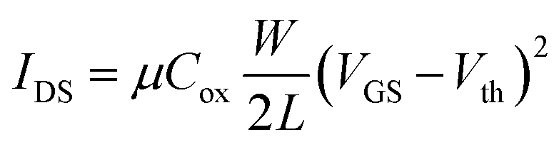
The unique role played by OFETs has for many years attracted enormous research interest. This is due to the possibility of achieving a low cost, easily processible, flexible and light-weight device with high performance at low temperatures by a solution method.1–4 In order to have an OFET with improved performance, it is important to prepare a high surface quality and uniform thin film gate dielectric that possesses a high-k value.5,6 This type of gate dielectric affords the fabrication of OFET with high field effect mobility (μ), a threshold voltage (Vth) which is close to zero and subthreshold slope (SS) that is as low as possible.Traditionally, 200 nm to 300 nm thick commercially available or home made silicon oxide (SiO2) film, thermally grown on a heavily doped n or p type silicon (Si) substrate is used as gate dielectric in OFETs.7–9 The k value for SiO2 is <4.0. This presents SiO2 as a low capacitance gate dielectric material which yields an OFET with low performance. The capacitance density of such a material can be improved by either reducing its thickness or increasing its k value as denoted in eqn (1)
 | (1) |
ZrO2,15,16 HfO2,17,18 Al2O3 (ref. 19) and TiO2 (ref. 20) are examples of inorganic high-k dielectric materials. However, for reasons such as interfacial mismatch and large leakage current exhibited by TiO2 due to its high permittivity value and small band gap14 and the formation of grain boundaries due to the low temperature crystallization of HfO2 and ZrO2,21 Al2O3 stands out as the most suitable inorganic metal oxide. Though Al2O3 has a moderate k value compared to the others, it has advantages such as large band gap and excellent thermal stability.22 Bilayer gate dielectric systems based on Al2O3 and their applications in OFETs have been widely reported over the years.23–25 However, an improvement in the performance of pentacene based OFETs due to the formation of SiO2/Al2O3 bilayer gate dielectric system resulting from the introduction of high-k Al2O3 buffer layer with decent surface properties on SiO2 has not been reported. The materials usually employed for this purpose are self-assemble monolayers (SAMs) and polymers26–28 which are organic and generally possess low k-values.
Preparation methods such as radio frequency (r.f.) magnetron sputtering,29,30 atomic layer deposition (ALD),31–33 chemical vapour deposition (CVD)34,35 and solution processing36–39 have been reported for Al2O3 gate dielectric. However, considering the tasking requirements such as high vacuum, high temperature and high cost needed for the sputtering, ALD and CVD methods, the solution processing route stands out as the most desirable as it does not require these conditions.
Though a few reports have been given on the solution processing of Al2O3 as gate dielectric in OFETs, a relatively high processing temperature especially at the annealing stage has so far been a limiting factor. Han et al.37 reported an annealing temperature of 400 °C as the requirement for the decomposition of the organic components in the Al2O3 precursors. 300 °C was also reported by Avis et al.36 has the required annealing temperature for the preparation of Al2O3. Peng et al.39 studied the application of amorphous alumina as gate dielectric in OFETs by demonstrating a facile low temperature solution method for the preparation of this material. They reported a maximum processing temperature of 180 °C. Polymeric nature of precursor materials could enhance the preparation of highly uniform thin buffer layer of Al2O3 on SiO2 by spin coating, thereby forming a bilayer gate dielectric system. This yields an improved equivalent k value for the resulting bilayer gate dielectric. It is known that improvements in the k value and surface properties of a gate dielectric enhance the mobility of the charge carriers in the active layer of an OFET.19,39–42
Solution–gelation (sol–gel) chemistry offers a mild route to the preparation of metal oxides.45 In this report, sol–gel chemistry which is based on low temperature polymerization of molecular precursors such as metal alkoxides M(OR)n43–45 via hydrolysis and condensation steps was adopted for the preparation of AlOx. Hydrolysis and condensation of alkoxides usually lead to the formation of metal oxo-polymers.46,47 The resulting polymeric gel was deposited by spin-coating and annealed at a maximum temperature of 150 °C to obtain an off-stoichiometric alumina (AlOx) thin film. Gradual decomposition of the organic components of the polymeric gel was measured as the annealing temperature increased using Fourier transform-infrared spectroscopy (FT-IR). The effect of surface modification on the performance of a pentacene based OFET was then studied by applying a thin film (20 nm) of the prepared AlOx as a top buffer layer on a 200 nm thick SiO2 which served as the bottom layer.
Results and discussion
Material preparation and characterization
The low temperature sol–gel process used in the preparation of our material followed the hydrolysis and condensation reaction pathway as shown in Scheme 1 below: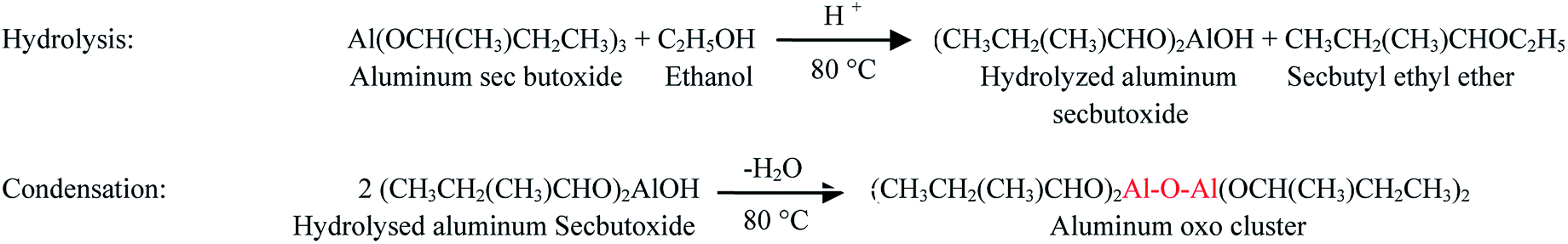 | ||
| Scheme 1 | ||
In Fig. 1(a), an FT-IR spectra showing the gradual decomposition of the organic components in the AlOx thin film is presented. It can be seen that the as-prepared material exhibits a broad peak around 3450 cm−1, a strong peak around 1467 cm−1 and a weak peak at 696 cm−1 for OH stretch and OH bend vibrations. This indicates the presence of OH group in large proportions majorly as a result of the solvent used. Weak peaks around 2935 cm−1 and a strong peak at 1573 cm−1 indicate the presence of C–H bonds as a result of the organic and metal–organic starting materials. C–O bonds in the precursor gel are also indicated by the peaks seen around 1058 cm−1. The stable peak observed at 578 cm−1 is attributed to the Al–O–Al bonds. A reduction in the peak intensities of the organic components can be observed as the annealing temperature increases while the AlOx peak shows a negligible variation in intensity. At 150 °C, there is a complete disappearance of the peaks attributed to the material's organic components leaving only the peak attributed to Al–O–Al.
 | ||
| Fig. 1 (a) FT-IR spectra showing the gradual decomposition of the organic components in the low temperature sol–gel processed AlOx thin film during annealing, (b) wide scan XPS analysis showing the chemical composition of the material annealed at 150 °C, (c) the peak for Al 2p core level observed at 74.6 eV binding energy and (d) the annealing temperature dependent peaks for O 1s core level observed at 531.2 eV and 532.2 eV binding energies. | ||
The chemical composition of the material was further analysed by X-ray photoelectron spectroscopy (XPS). The wide-scan XPS spectrum of the thin film annealed at 150 °C (Fig. 1(b)) reveals that the material consists of only Al and O without other hetero elements. The detailed Al spectrum of the thin film annealed at 150 °C (Fig. 1(c)) reveals a peak at 74.6 eV which is attributed to Al 2p core level. Though a peak for Al 2s core level is also observed at 120.1 eV on the wide scan (Fig. 1(b)), it is a common practice to use the Al 2p peak to analyse samples containing aluminum39,48–50 because plasmon loss peaks from the Al 2p transition usually interfere with the Al 2s peak making the quantification of such peak complicated.51 Fig. 1(d) shows the detailed XPS spectra of O 1s core level for AlOx thin film at ambient and at different annealing temperatures. The peaks were further deconvoluted to show the different environments of the O 1s core level at 531.2 eV (Al–O–Al)52 and about 532.2 eV (Al–OH and Al–OR).52,53 These results show that the formation of Al–O–Al bridge is effectively enhanced as the annealing temperature rises from ambient to 150 °C. This is attributed to the formation of more pure Al–O–Al bridge due to the decomposition of the Al–OH and Al–OR components as the anneal temperature increases. This agrees well with the FT-IR results (Fig. 1(a)) as it indicates that the hydroxy and alkoxy groups become unstable at higher temperature and are decomposed. We determined the stoichiometry of the material annealed at 150 °C by investigating the Al![[thin space (1/6-em)]](https://www.rsc.org/images/entities/char_2009.gif) :O ratio. This was done by processing the data with the Casa XPS program (Casa Software Ltd, UK). Peak areas for Al 2p and O 1s core levels were determined by employing a Shirley-type background. The relative sensitivity factors (RSF) provided in the software library were used for quantifying elements.
:O ratio. This was done by processing the data with the Casa XPS program (Casa Software Ltd, UK). Peak areas for Al 2p and O 1s core levels were determined by employing a Shirley-type background. The relative sensitivity factors (RSF) provided in the software library were used for quantifying elements.
As shown in Table S1,† we obtained an Al:O ratio of 1:1.65 which is similar to values earlier reported by Peng et al.39 Although the expected atomic ratio is 1:1.5 for a pure Al2O3, the excess oxygen may be as a result of the flexibility in the variation of chemical compositions of amorphous materials without a significant change in phase.
No obvious diffraction peak can be observed in the XRD pattern of the film annealed at 150 °C (Fig. S2†). This confirms the amorphous nature of the material. The FT-IR, XPS and XRD analyses show that a pure off-stoichiometric amorphous AlOx thin film which is suitable for device applications such as gate dielectric in OFETs can be successfully prepared by our method.
It is important that the surface of the material serving as gate dielectric in OFETs be as smooth as possible as the surface properties determine the morphology and the charge carrier mobility of the active layer and the general performance of the device. We therefore conducted a comparative surface scan on the SiO2 layer and the 20 nm AlOx thin film deposited on SiO2 layer and annealed at 150 °C to form a SiO2/AlOx bilayer system. This was done by using AFM in the tapping mode. Fig. 2 shows the AFM images of the two forms of gate dielectric. As seen in Fig. 2(a) the thermally grown SiO2 layer exhibits a greater roughness (rms 0.23 nm) while in Fig. 2(b) the SiO2/AlOx bilayer system exhibits a much lower roughness (rms 0.11 nm). Hence, due to its polymeric nature, the AlOx gel obtained from the low temperature sol–gel process can easily form a uniform and homogenous thin film on the thermally grown SiO2 layer using the spin coating technique. This therefore makes the material suitable for applications as gate dielectric and dielectric buffer layer in OFETs.
 | ||
| Fig. 2 Tapping mode AFM surface scan of (a) the SiO2 single layer with a root-mean-square (rms) roughness of 0.23 nm and (b) the 20 nm AlOx thin film deposited on SiO2 layer and annealed at 150 °C with an rms roughness of 0.11 nm. | ||
Material's dielectric properties
To characterize the changes in dielectric properties such as leakage current density and k value of thermally grown SiO2 gate dielectric as a result of the deposition of a top buffer layer of AlOx, simple capacitors having a SiO2 single layer and a SiO2/AlOx bilayer with MIM device structures Si/SiO2/Au and Si/SiO2/AlOx/Au respectively were fabricated. Their current–voltage characteristics and frequency dependent capacitance (C–F) curves where obtained. Fig. 3(a) shows the leakage current density as a result of the applied bias voltage for both the SiO2 single layer and the SiO2/AlOx bilayer gate dielectric materials. It can be seen that the SiO2/AlOx bilayer with a field strength of 1.8 MV cm−1 shows better insulating properties with a low leakage current density (<1 × 10⁻⁸ A cm−2) while the SiO2 single layer with a field strength of 2 MV cm−1 shows a relatively higher leakage current density (<1 × 10⁻⁶ A cm−2). Both measurements were taken by applying a bias voltage of 40 V over a contact area of 0.09 cm2. | ||
| Fig. 3 (a) The leakage current density as a result of the applied bias voltage for both the SiO2 single layer and the SiO2/AlOx bilayer gate dielectric materials and (b) the frequency dependent capacitance density measured for the device made with SiO2 single layer and SiO2/AlOx bilayer showing standard deviation based on five rounds of measurements in each case. | ||
To prevent the injection of charge carriers into an oxide gate dielectric the band potential barrier must be greater than 1 eV.22 SiO2 which has a band gap of 9 eV could therefore be said to be a suitable gate dielectric material as it has high barriers for electrons and holes. However its k value is considerably low to effectively perform this function. The reduction in leakage current observed for SiO2/AlOx bilayer is due to the increase in thickness of the double layer system and the increase in the equivalent dielectric constant due to the addition of a high-k top layer (in this case AlOx). The tunnelling current in a gate dielectric material decreases exponentially as the thickness and the k value of the dielectric layer increase. Fig. 3(b) shows the standard deviation curves of frequency dependent capacitance of the device made with SiO2 single layer and SiO2/AlOx bilayer. The measurements were repeated five times in each case by applying a zero bias voltage on the Au top electrode while we ground the Si substrate. The capacitance density for both devices were observed to be stable over a wide range of frequencies. Lower capacitance density values were obtained for the bilayer gate dielectric compared to the single layer dielectric. As depicted in eqn (2), this is as a result of the series connection between the SiO2 and AlOx layers.
 | (2) |
Using eqn (1) and averaged Ci of 17.30 nF cm−2 (SiO2) and 16.62 nF cm−2 (SiO2/AlOx) obtained from Fig. 3(b) over a frequency range of 20 Hz to 106 Hz, the extracted k values for the SiO2 (200 nm) single layer and SiO2/AlOx bilayer (220 nm) dielectric are 3.9 and 4.13 respectively. This increased k value in the bilayer alleviates the problem of tunnelling current.
Device properties
To explore the effect of this surface modification of SiO2 gate dielectric, pentacene based OFET was fabricated using the SiO2/AlOx bilayer as gate dielectric (Fig. S1†). OFET having SiO2 single layer gate dielectric was also fabricated as a reference device. Characterization was done by using the standard MOSFET model in the saturation region. The devices have a pentacene active layer channel length (L) of 70 μm and a channel width (W) of 1500 μm. 20 devices were fabricated each for the OFETs with and without AlOx buffer layer. The results obtained were averaged and presented in Table 1. Fig. 4(a) and (c) show the room temperature (300 K) transfer characteristics of devices without and with AlOx buffer layer respectively. The transfer characteristics are logarithmic plots of −IDS vs. VGS and plots of (−IDS)1/2 vs. VGS taken at VDS = −30 V. The devices' transfer characteristics were also taken at other temperatures (280 K, 260 K, 240 K, 220 K and 200 K) as shown in (Fig. S3a and b†). The room temperature output characteristics of the devices are also presented in Fig. 4(b) and (d). From the parameters obtained we extracted the field effect mobility in pentacene active layer of the devices using eqn (3).
 | (3) |
| Device | μ (cm2 V−1 s−1) | Vth (V) | SS (V per decade) | On/off current | Vto (V) |
|---|---|---|---|---|---|
| With AlOx buffer layer | 0.81 ± 0.02 | −0.69 ± 0.03 | 0.10 ± 0.03 | 1.00 ± 0.1 (×103) | 0.20 ± 0.02 |
| Without AlOx buffer layer | 0.28 ± 0.04 | −2.10 ± 0.06 | 0.40 ± 0.08 | 4.00 ± 0.2 (×102) | 1.90 ± 0.05 |
 | ||
| Fig. 4 (a & b) The transfer curve and output characteristics of OFET without AlOx buffer layer. (c & d) The transfer curve and output characteristics of OFET with AlOx buffer layer. The transfer curves are logarithmic plots of −IDS vs. VGS and a plot of (−IDS)1/2 vs. VGS taken at VDS = −30 V and the output characteristics represent the drain–source current (IDS) vs. drain–source voltage (VDS) of the devices for each value of gate–source voltage (VGS) which is increased steadily from 0 V to −30 V at an interval of 6 V. | ||
In eqn (3), μ denotes the field effect mobility, Vth, threshold voltage, Cox, capacitance of oxide gate dielectric per unit area, W and L denote the channel width and channel length respectively. Arrhenius plots of the corresponding mobilities as a function of temperature (T) is given in Fig. 5. Therefore, using eqn (4), parameters such as trap free mobilities (μ0) and their corresponding activation energies Ea can be extracted from the plots.
|
μFET = μ0exp(−Ea/KT)
| (4) |
 | ||
| Fig. 5 Arrhenius plots of mobilities as a function of temperature for devices fabricated with and without AlOx buffer layer. | ||
K, in eqn (4) is the Boltzmann constant and T is the temperature. It can be seen from Table 1 that the device with AlOx exhibits an averaged mobility value of 0.81 cm2 V−1 s−1 which is almost four times higher than that of the reference device (0.28 cm2 V−1 s−1). It can also be observed that the other parameters show improvements for the device with AlOx relative to the reference device.
The growth of pentacene is known to be sensitive to the gate dielectric surface.54 Since the oxide gate dielectric is in direct contact with the active layer, the charge carrier induction produced by the gate occurs at the active layer/oxide gate dielectric interface. Unlike the polycrystalline SiO2 which could be associated with defects such as oxide grain boundaries, the AlOx prepared and used in this work does not possess grain boundaries as it is amorphous (Fig. S2†). This amorphous material has advantages over the polycrystalline SiO2. Such material might be able to configure its interface bonding to minimize the number of interface defects. It is possible to gradually vary the composition of an amorphous oxide without creating a new phase. Amorphous oxides and their dielectric constants are also isotropic, thus fluctuations in polarization from differently oriented oxide grains which could scatter charge carriers does not occur.
Fig. 6 show the morphologies (XRD patterns and AFM images (insets)) of pentacene layer grown on both SiO2/AlOx bilayer and SiO2 single layer gate dielectrics. The same peak pattern was observed for the pentacene layer with and without AlOx underlayer. However, a closer look at the XRD patterns reveals a slight increase in peak intensities for the pentacene layer grown on the SiO2/AlOx bilayer indicating that the AlOx underlayer is favourable for enhanced crystallization of the pentacene layer. Furthermore, it can be seen in the insets of Fig. 6(a) and (b) that the pentacene film has significantly larger grain size on SiO2/AlOx bilayer surface when compared to the film on the SiO2 single layer surface.
 | ||
| Fig. 6 XRD spectra of pentacene films grown on: (a) SiO2/AlOx bilayer and (b) SiO2 single layer gate dielectric surfaces. Insets are the corresponding AFM images. | ||
The origin of this variation in pentacene morphology which is a vital factor for charge carrier transport along the pentacene structure can be traced to the surface energies (γs) of the single layer and bilayer gate dielectrics. To obtain γs for SiO2/AlOx bilayer and SiO2 single layer, the contact angles of two test liquids (water and diiodomethane) on the surfaces of the two dielectrics were measured by using a goniometer (G 10, Krüss) equipped with an image capture software (Drop Shape Analysis 1.0 software). As shown in Fig. S4a and b,† water contact angles for SiO2/AlOx bilayer and SiO2 single layer were 42.6° and 64.6° respectively.
Diiodomethane also made contact angles of 24.6° and 34.3° on the bilayer and single layer dielectrics respectively. γs for each dielectric was extracted from the Owen, Wendt, Rabel and Kaelble (OWRK) model which is based on Young's equation (eqn (5)) by fitting the measured values of contact angles.54
|
γs = γsl + γlcosθ
| (5) |
| γsl = γs + γl − 2[(γds)1/2(γdl)1/2 + (γps)1/2(γpl)1/2] | (6) |
In the above equations, γsl denotes the interfacial energy between the solid phase (dielectric surface) and the liquid phase (test liquid), γl is the surface energy of each test liquid and the superscripts d and p in eqn (6) are their dispersive and polar components respectively. The γs value obtained for our prepared SiO2/AlOx bilayer (41.3 mJ m−2) is lower than γs value (48.0 mJ m−2)54,55 reported for pentacene. As a result, the pentacene molecules showed better attraction to the bilayer dielectric surface than they do to each other.
This induced a wider coverage of the resulting large pentacene crystallites on the bilayer gate dielectric as shown in the inset of Fig. 6(a). Conversely, the obtained surface energy for SiO2 single layer (55.8 mJ m−2) is higher than that of pentacene. Consequently, the pentacene molecules exhibited better attraction for each other than for the SiO2 single layer gate dielectric. The pentacene molecules therefore tend to self-assemble as they are deposited on the SiO2 single layer dielectric. This resulted in the formation of small pentacene crystallites (inset of Fig. 6(b)) with enormous volume of grain boundaries which act as traps for charge carriers and contribute to the lower mobility observed in the OFET fabricated without the AlOx buffer layer.
The surface of the underlying gate dielectric layer also has influences on the structural properties of the pentacene crystallites. An induction of structural inhomogeneities in the pentacene crystal structure could lead to limited charge transport.56 Previous studies have shown that hole transport in pentacene crystallites is based on conducting paths formed by π-orbital overlap.57 Such overlap was found to be negligible along the c-axis of the molecule. It was however found to be very effective along the in-plane, ab direction. In addition, herringbone molecular packing have been found to be responsible for different charge transport efficiencies along the face-to-face and face-to-edge orientations of the π-stacking.58
As shown in Fig. 5, it is seen that the mobilities of pentacene-OFETs fabricated on both SiO2/AlOx bilayer and SiO2 single layer exhibited linear Arrhenius relationship with the inverse of temperature (T). This is in accord with previous reports that charge carrier transport in organic semiconductors increases with T.59 This is because charge transport is generally limited by localized trap states which produce a “multiple trapping and thermal release” mode of transport.56 It involves the instantaneous capture of free carriers arriving at traps with a probability close to unity and a thermally-activated release of such trapped carriers.
Therefore, we investigated the origin of improved mobility in the OFET with AlOx buffer layer. This was done by studying the linear relationship between lnμ and 1/T for the pentacene-OFETs formed on SiO2/AlOx bilayer and SiO2 single layer in Fig. 5. The higher Ea (72 meV) observed for the device without AlOx buffer layer corresponds to a broader and deeper trap distribution with respect to the localized energy levels. It shows that there exist numerous grain boundaries (inset of Fig. 6(b)) which lead to more defects in the pentacene layer of the device without AlOx buffer layer, unlike in the device with AlOx buffer layer which exhibited wider coverage and less grain boundary. As a result, there is a reduction of charge carrier transport in the OFET without AlOx buffer layer. This agrees well with previous reports.54,56
The superior surface properties of the amorphous AlOx buffer layer ensures that negligible trapped charges exist in the active layer/gate dielectric interface. This is confirmed by the near zero turn-on voltage (Vto) obtained for the device with AlOx buffer layer (Fig. 4(c)). The improved equivalent dielectric constant of the SiO2/AlOx bilayer gate dielectric allows higher concentration of charge carriers to accumulate in the pentacene active layer for the same applied voltage when compared with the device with single SiO2 layer exhibiting lower k value. This accumulation of the charge carriers causes the Fermi level of the electrodes to move towards the band edge of the active layer. This causes the injection of high density of carriers which are free to move with high mobility into the active layer. Therefore, the SiO2/AlOx bilayer gate dielectric with decent surface properties and improved k value is capable of improving carrier mobility in the pentacene active layer of OFETs.
Conclusion
In conclusion, we have achieved the preparation of an OFET with improved device parameters by carrying out a surface modification of SiO2 gate dielectric. This was made possible by the introduction a low temperature sol–gel processed thin film of amorphous AlOx prepared in this work. The surface modification produced a SiO2/AlOx bilayer system as the gate dielectric. The bilayer dielectric system exhibits a smooth surface with rms of 0.11 nm, an equivalent k value of 4.13, a capacitance density of 16.62 nF cm−2 and a low leakage current density <1 × 10⁻⁸ A cm−2. Using the SiO2/AlOx bilayer system as the gate dielectric, the fabricated pentacene-based OFET exhibited a field effect mobility of 0.81 cm2 V−1 s−1. This device performance is improved compared to that of the SiO2 single layer gate dielectric which gave a mobility of 0.28 cm2 V−1 s−1. The surface modification of SiO2 gate dielectric using a low-temperature sol–gel processed amorphous AlOx provides a feasible approach for improving the properties of the gate dielectric and the overall device performance of OFETs.Acknowledgements
We acknowledge financial support from the Natural Science Foundation of China (No. 61307036 and 61177016) and from the Natural Science Foundation of Jiangsu Province (No. BK20130288). This project is also funded by the Collaborative Innovation Center of Suzhou Nano Science and Technology, the Priority Academic Program Development of Jiangsu Higher Education Institutions (PAPD) and China Scholarship Council (CSC).Notes and references
- B. Shaik, J.-H. Han, D. J. Song, H.-M. Kang, Y. B. Kim, C. E. Park and S.-G. Lee, RSC Adv., 2016, 6, 4070 RSC.
- M. Devynck, P. Tardy, G. Wantz, Y. Nicolas, L. Vellutini, C. Labrugere and L. Hirsch, Appl. Phys. Lett., 2012, 100, 053308 CrossRef.
- S. Faraji, T. Hashimoto, M. L. Turner and L. A. Majewski, Org. Electron., 2015, 17, 178 CrossRef CAS.
- M. W. Alam, Z. Wang, S. Naka and H. Okada, Appl. Phys. Lett., 2013, 102, 061105 CrossRef.
- L. Miozzo, A. Yassar and G. Horowitz, J. Mater. Chem., 2010, 20, 2513 RSC.
- D. Q. Wu, H.-S. Zhao, J.-C. Yao, D.-Y. Zhang and A.-M. Chang, J. Inorg. Mater., 2008, 23, 865 CrossRef CAS.
- F. Zhou, H. P. Lin, J. Li, L. Zhang, X. W. Zhang, D. B. Yu, X. Y. Jiang, Z. L. Zhang and J. H. Zhang, J. Optoelectron. Adv. Mater., 2011, 13, 791 Search PubMed.
- A. N. Aleshin, I. P. Shcherbakov, A. S. Komolov, V. N. Petrov and I. N. Trapeznikova, Org. Electron., 2015, 16, 186 CrossRef CAS.
- J. Chang, J. Li, K. L. Chang, J. Zhang and J. Wu, RSC Adv., 2013, 3, 8721 RSC.
- H. S. Tan, T. Cahyadi, Z. B. Wang, A. Lohani, Z. Tsakadze, S. Zhang, F. R. Zhu and S. G. Mhaisalkar, IEEE Electron Device Lett., 2008, 29, 698 CrossRef CAS.
- S. Bang, S. Lee, S. Jeon, S. Kwon, W. Jeong, H. Kim, I. Shin, H. J. Chang, H.-H. Park and H. Jeon, Semicond. Sci. Technol., 2009, 24, 025008 CrossRef.
- Y.-H. Chou, Y.-C. Chiu and W.-C. Chen, Chem. Commun., 2014, 50, 3217 RSC.
- A. L. Deman and J. Tardy, Mater. Sci. Eng., C, 2006, 26, 421 CrossRef CAS.
- Y. Su, C. Wang, W. Xie, F. Xie, J. Chin, N. Zhao and J. Xu, ACS Appl. Mater. Interfaces, 2011, 3, 4662 CAS.
- Y. Wang and H. Kim, Org. Electron., 2012, 12, 2997 CrossRef.
- J.-W. Lee, B.-K. Ju, J. Jang, Y.-S. Yoon and J.-K. Kim, J. Mater. Sci., 2007, 42, 1026 CrossRef CAS.
- M. R. Yisokay, J. J. Chambers, A. L. P. Rotondaro, A. Shanware and L. Colombo, Appl. Phys. Lett., 2002, 80, 3183 CrossRef.
- Y. B. Yoo, J. H. Park, K. H. Lee, H. W. Lee, K. M. Song, S. J. Lee and H. K. Baik, J. Mater. Chem. C, 2013, 1, 1651 RSC.
- X.-H. Zhang, B. Domercq, X. Wang, S. Yoo, T. Kondo, Z. L. Wang and B. Kippelen, Org. Electron., 2007, 8, 718 CrossRef CAS.
- Q. Xie, D. Deduytsche, M. Schaekers, M. Caymax, A. Delabie, X.-P. Qu and C. Detavernier, Appl. Phys. Lett., 2010, 97, 112905 CrossRef.
- C. L. Dezelah, J. Niinisto, K. Kukli, F. Munnik, J. Lu, M. Ritata, M. Leskela and L. Niinisto, Chem. Vap. Deposition, 2008, 14, 358 CrossRef CAS.
- J. Robertson, Eur. Phys. J.: Appl. Phys., 2004, 28, 265 CrossRef CAS.
- X. Ye, H. Lin, X. Yu, S. Han, M. Shang, L. Zhang, Q. Jiang and J. Zhong, Synth. Met., 2015, 209, 337 CrossRef CAS.
- Y. Baek, S. Lim, L. H. Kim, S. Park, S. W. Lee, T. H. Oh, S. H. Kim and C. E. Park, Org. Electron., 2016, 28, 139 CrossRef CAS.
- J. Jang, S. Nam, W. M. Yun, C. Yang, J. Hwang, T. K. An, D. S. Chung and C. E. Park, J. Mater. Chem., 2011, 21, 12542 RSC.
- S. A. DiBenedetto, A. Facchetti, M. A. Ratner and T. J. Marks, Adv. Mater., 2009, 21, 1407 CrossRef CAS.
- S. H. Noh, W. Choi, M. S. Oh, D. K. Hwang, K. Lee, S. Im, S. Jang and E. Kim, Appl. Phys. Lett., 2007, 90, 253504 CrossRef.
- J. Roh, C. Kang, J. Kwak, C. Lee and B. J. Jung, Appl. Phys. Lett., 2014, 104, 173301 CrossRef.
- M. S. Oh, D. K. Hwang, K. Lee, S. Im and S. Yi, Appl. Phys. Lett., 2007, 90, 173511 CrossRef.
- C. Lin, J. Kang, D. Han, D. Tian, W. Wang, J. Zhang, M. Liu, X. Liu and R. Han, Microelectron. Eng., 2003, 66, 830 CrossRef CAS.
- B.-U. Hwang, D.-L. Kim, S.-W. Cho, M.-G. Yun, H.-J. Kim, Y.-J. Kim, H.-K. Cho and N. E. Lee, Org. Electron., 2014, 15, 1458 CrossRef CAS.
- Z. Chai, Y. Liu, J. Li, X. Lu and D. He, RSC Adv., 2014, 4, 50503 RSC.
- X. Ding, H. Zhang, H. Ding, J. Zhang, C. Huang, W. Shi, J. Li, X. Jiang and Z. Zhang, Superlattices Microstruct., 2014, 76, 156 CrossRef CAS.
- Q. Y. Shao, A.-D. Li, H.-Q. Ling, D. Wu, Y. Wang, Y. Feng, S.-Z. Yang, Z.-G. Liu, M. Wang and N.-B. Ming, Microelectron. Eng., 2003, 66, 842 CrossRef CAS.
- Y.-I. Ogita, S. Ohsone, T. Kudoh and F. Sakamoto, Thin Solid Films, 2008, 516, 836 CrossRef CAS.
- C. Avis and J. Jang, J. Mater. Chem., 2011, 21, 10649 RSC.
- K.-K. Han and S. Seo, Jpn. J. Appl. Phys., 2011, 50, 04DK17 CrossRef.
- D. X. Xia and J. B. Xu, J. Phys. D: Appl. Phys., 2010, 43, 442001 CrossRef.
- J. Peng, Q. Sun, S. Wang, H.-Q. Wang and W. Ma, Appl. Phys. Lett., 2013, 103, 061603 CrossRef.
- Z. Wang, M. W. Alam, Y. Lou, S. Naka and H. Okada, Appl. Phys. Lett., 2012, 100, 043302 CrossRef.
- L.-K. Mao, J.-C. Hwang and Y.-L. Chueh, Org. Electron., 2014, 15, 2400 CrossRef CAS.
- Y. Lou, M. F. Xu, Z. Wang, S. Naka, H. Okada and L. S. Liao, Appl. Phys. Lett., 2013, 102, 113305 CrossRef.
- C. J. Brinker, B. C. Bunker, D. R. Tallant, K. J. Ward and R. J. Kirkpatrick, ACS Symp. Ser., 2009, 360, 314 CrossRef.
- S. Park, K.-H. Kim, J.-W. Jo, S. Sung, K.-T. Kim, W.-J. Lee, J. Kim, H. J. Kim, G.-R. Yi, Y.-H. Kim, M.-H. Yoon and K. P. Sung, Adv. Funct. Mater., 2015, 25, 2807 CrossRef CAS.
- G. J. Owens, R. K. Singh, F. Foroutan, M. Alqaysi, C.-M. Han, C. Mahapatra, H.-W. Kim and J. C. Knowles, Prog. Mater. Sci., 2016, 77, 1 CrossRef CAS.
- F. Babonneau, S. Dire, L. Bonhomme-Coury and J. Livage, ACS Symp. Ser., 2009, 572, 134 CrossRef.
- T. Cottineau, M. Richard-Plouet, A. Rouet, E. Puzenat, H. Sutrisno, Y. Piffard, P.-E. Petit and L. Brohan, Chem. Mater., 2008, 20, 1421 CrossRef CAS.
- P. K. Nayak, J. A. Caraveo-Frescas, Z. Wang, M. N. Hedhili, Q. X. Wang and H. N. Alshareef, Sci. Rep., 2014, 4, 4672 Search PubMed.
- J. Peng, Q. Sun, Z. Zhai, J. Yuan, X. Huang, Z. Jin, K. Li, S. Wang, H. Wang and W. Ma, Nanotechnology, 2013, 24, 484010 CrossRef PubMed.
- S. H. Baek, G.-H. Nam and I. K. Park, RSC Adv., 2015, 5, 59823 RSC.
- CasaXPS Manual 2.3.15 Introduction to XPS and AES, http://www.casaxps.com/ebooks/ebooks.htm, accessed March 2016.
- K. Lee, J. S. Jur, D. H. Kim and G. N. Parsons, J. Vac. Sci. Technol., A, 2012, 30, 01A163 Search PubMed.
- Y.-W. Wang, G.-Y. Tseng, L.-Y. Chiu, B.-R. Lin, Y.-Y. Lin, T. W. Haung, W.-Y. Chou, L. Horng and H.-L. Cheng, J. Mater. Chem. C, 2014, 2, 7752 RSC.
- S. H. Kim, M. Jang, H. Yang and C. E. Park, J. Mater. Chem., 2010, 20, 5612 RSC.
- J. E. Northrup, M. L. Tiago and S. G. Louie, Phys. Rev. B: Condens. Matter Mater. Phys., 2002, 66, 121404 CrossRef.
- D. Braga and G. Horowitz, Adv. Mater., 2009, 21, 1473 CrossRef CAS.
- A. Troisi and G. Orlandi, J. Phys. Chem. B, 2005, 109, 1849 CrossRef CAS PubMed.
- S. M. Ryno, C. Risko and J.-L. Bredas, J. Am. Chem. Soc., 2014, 136, 6421 CrossRef CAS PubMed.
- M. Gruber, S.-H. Jung, S. Schott, D. Venkateshvaran, A. J. Kronemeijer, J. W. Andreasen, C. R. McNeill, W. W. H. Wong, M. Shahid, M. Heeney, J.-K. Lee and H. Sirringhaus, Chem. Sci., 2015, 6, 6949 RSC.
Footnote |
| † Electronic supplementary information (ESI) available: It includes; experimental section, device structure of the pentacene based OFET with AlOx as gate dielectric buffer layer, Table of peak parameters of Al 2p and O 1s core levels and the quantified Al:O ratio in AlOx thin film annealed at 150 °C, XRD pattern of the AlOx thin film annealed at 150 °C confirming the amorphous nature of the material, temperature dependent transfer curves of OFETs with and without AlOx buffer layer and images of contact angle values of water on SiO2/AlOx bilayer, water on SiO2 single layer, diiodomethane on SiO2/AlOx bilayer and diiodomethane on SiO2 single layer. See DOI: 10.1039/c6ra02700h |
| This journal is © The Royal Society of Chemistry 2016 |