
All electrochemical fabrication of MoS2/graphene counter electrodes for efficient dye-sensitized solar cells†
Shengli Li‡
a,
Huihua Min‡b,
Feng Xu*ac,
Ling Tongd,
Jing Chene,
Chongyang Zhua and
Litao Sun*ac
aSEU-FEI Nano-Pico Center, Key Laboratory of MEMS of the Ministry of Education, Southeast University, Nanjing 210096, China. E-mail: fxu@seu.edu.cn; slt@seu.edu.cn; Fax: +86-25-83792939; Tel: +86-25-83792632
bElectron Microscope Laboratory, Nanjing Forestry University, Nanjing 210037, China
cCenter for Advanced Materials and Manufacture, Joint Research Institute of Southeast University and Monash University, Suzhou 215123, China
dJiangnan Graphene Research Institute, Changzhou 213149, China
eSchool of Electronic Science & Engineering, Southeast University, Nanjing 210096, China
First published on 31st March 2016
Abstract
Exploring inexpensive, high-efficiency counter electrodes (CEs) that rival the traditional platinum (Pt) CEs for dye-sensitized solar cells (DSSCs) is a great challenge. Here we report an all electrochemical strategy to facilely prepare MoS2/graphene composite films that directly act as CEs of DSSCs without needing additional post-treatment. This strategy consists of electrodeposition and electroreduction of graphene oxide (GO) and subsequent electrodeposition of MoS2 on reduced GO layers. The as-prepared composite CEs are characterized by Raman spectroscopy, scanning electron microscopy (SEM), and transmission electron microscopy (TEM). The DSSCs based on optimized MoS2/graphene CEs exhibit a high power conversion efficiency (PCE) of 8.01%, which is comparable to 8.21% of the Pt CE. The superior PCE is indubitably attributed to the superior electrocatalytic activity of the composite CEs, as corroborated by their cyclic voltammetry (CV), Tafel polarization curves and electrochemical impedance spectra (EIS). Our all electrochemical strategy also holds promise in preparing graphene-enhanced chalcogenide functional composite films.
Introduction
Dye-sensitized solar cells (DSSCs) have been extensively studied in the past few decades because of their low cost, simple fabrication process, and high power conversion efficiency (PCE).1–3 As one of the important components in DSSCs, counter electrodes function as the catalyst to collect electrons from an external circuit and catalyze the reduction of the redox couple (I−/I3−) in the electrolyte. Platinum (Pt) is the most commonly used CE material due to its high electrocatalytic activity to the reduction of I3− to I−.4,5 However, Pt is expensive and rare, paving the way for exploring alternative inexpensive CE materials.6–8 To date, carbon materials,9–11 inorganic compounds,12–14 conductive polymers15–17 and composite materials18–20 have been successfully developed for applications as CEs of DSSCs.Recently, molybdenum disulfide (MoS2) has demonstrated its electrocatalytic activity for I3− reduction when used as the CEs.21,22 However, in addition to the electrocatalytic activity, electrical conductivity is another important issue researchers have to consider. In this regard, graphene is frequently incorporated into the MoS2 material to enhance its electrical conductivity as well as electrocatalytic activity owing to its superior electron transport property and large specific surface area.23–26 For instance, Liu et al.27 first reported the synthesis of MoS2/grapheme nanocomposite by mixing graphene oxide (GO) nanosheets with a solution of ammonium tetrathiomolybdate and then converting the as-obtained intermediate precipitate into MoS2/rGO in a H2 flow at 650 °C for 1 h. Lin et al.28 reported a transparent MoS2 and graphene nanosheet composite by thermal hydrolysis/dissociation of thiourea in the presence of GO and sodium molybdate. Yue et al.29 used a ball milling method to mix MoS2 powder and multi-layer graphene nanopowder. However, all these cases need additional fabrication procedures of the CEs such as electrophoresis deposition, drop-casting, and doctor blade method, which inevitably introduces undesired high-temperature annealing and results in time-consuming.
Here, we report an all electrochemical strategy to facilely prepare MoS2/graphene composite films that directly act as CEs of the DSSCs without needing additional post-treatment. This approach includes two main steps, as illustrated in Scheme 1. First, conductive graphene layer was deposited on the FTO substrate by electrochemical reduction of GO in aqueous dispersion. Secondly, MoS2 nanoparticles were subsequently deposited on the conductive surface of graphene layer through electrochemical deposition of ammonium thiomolybdate. The proposed all electrochemical strategy is very facile and quick, which just needs a few minutes to synthesize MoS2/graphene composite. Moreover, the resultant MoS2/graphene composite CE was demonstrated to have an improved electrocatalytic activity with the cell efficiency of 8.01%. To the best of our knowledge, it is the first time that this all electrochemical strategy was used in fabricating MoS2/graphene composite CE. It also provides an idea when synthesizing graphene-enhanced chalcogenide functional composite films.
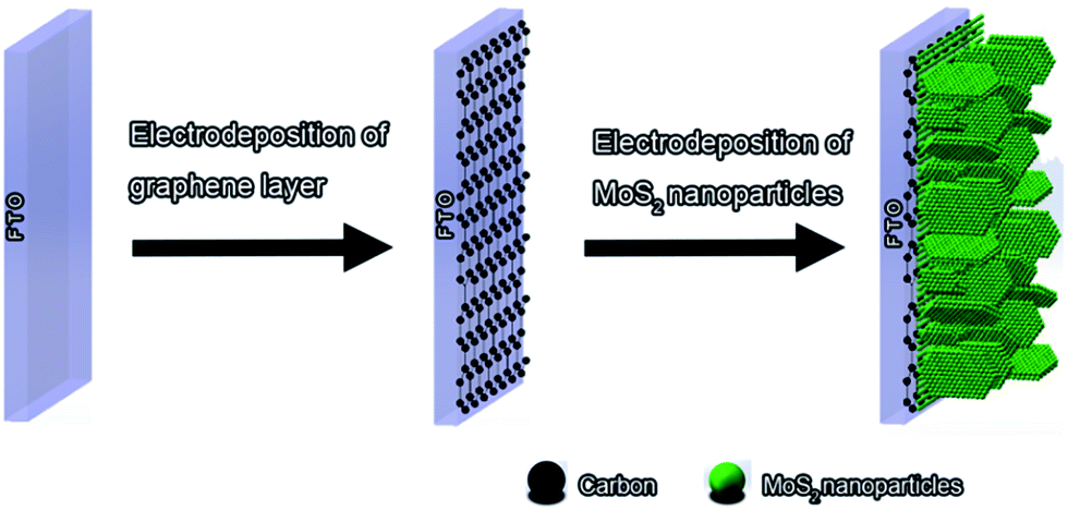 | ||
| Scheme 1 Schematic of the all electrochemical fabrication approach. This strategy consists of electrodeposition and electroreduction of graphene oxide (GO) and subsequent electrodeposition of MoS2 on reduced GO layers. | ||
Experimental
Preparation of counter electrodes
As illustrated in Scheme 1, all of our CEs were prepared by electrochemical deposition except Pt CE, which was purchased from Dalian HepatChroma Solartech Co. Ltd. To obtain MoS2/graphene CE, first, 80 mg GO, which was synthesized through a modified Hummers' method,30 and 1 g lithium perchlorate (LiClO4) were added to 40 ml deionized water, and ultrasonically dispersed for 60 min. Then graphene layer was obtained through electrochemical reduction of GO at a constant potential of −1.2 V in the solution for certain time (20–160 seconds). After that, MoS2 nanoparticles were further electrodeposited on the surface of graphene layer at a constant potential of −1 V for 5 min in a mixed solution of 0.005 M (NH4)2MoS4 and 0.1 M KCl. The deposition time of MoS2 was chosen to be 5 min because we got the highest cell efficiency of DSSCs with that MoS2 CEs. These steps were conducted on a CHI660D Electrochemical Workstation (CH instrument, Inc, USA) which consists of a FTO as the working electrode, Pt as the counter electrode, and SCE as the reference electrode. Besides, the pure MoS2 CE was directly obtained by electrodepositing MoS2 on FTO substrate at a constant potential of −1 V for 5 min in a mixed solution of 0.005 M (NH4)2MoS4 and 0.1 M KCl.Fabrication of DSSCs
TiO2 photoanodes were prepared by the screen-printing technique. Then they were immersed into 0.3 mM ethanol solution of ruthenium dye N719 at 45 °C for 6 h. After that, a sandwich-type cell was obtained by fabricating the dye-sensitized TiO2 photoanode with a CE, which were separated by a hot-melt Surlyn film (60 μm thick) and sealed through hot-pressing. Finally, the redox electrolyte which contains 0.1 M LiI, 0.05 M I2, 0.3 M 1,2-dimethyl-3-propylimidazolium iodine, and 0.5 M tert-butylpyridine in 3-methoxypropionitrile was injected into the space between the two electrodes.Characterization
Phase identification of the products was characterized by X-ray diffractometer (XRD, ARL XTRA, Thermo Electron Co., USA) with Cu Kα radiation as the X-ray source. Raman spectroscopy was conducted on Renishaw laser Raman spectrometer, using a laser source of 488 nm. During X-ray photoelectron spectroscopy (XPS) measurement, Mg Kα radiation (1253.6 eV) with power of 200 W and pass energy of 50.0 eV was used. The surface morphology and microstructure of the CEs were examined by a scanning electron microscope (SEM, JSM-7600F, JEOL, Japan) and a transmission electron microscope (TEM, FEI Titan 80–300 at 300 kV). Cyclic voltammetry (CV) was carried out on the CHI-660D electrochemical workstation mentioned above in a three-electrode system with an anhydrous acetonitrile (ACN) solution of 0.1 M LiClO4, 10 mM LiI, and 1 mM I2 at a scan rate of 50 mV s−1, using Pt as the counter electrode, a SCE as the reference electrode, and the as-prepared CEs as the working electrode. To exam Tafel polarization curves and electrochemical impedance spectra (EIS) of the CEs, the symmetric dummy cells were used. Tafel polarization curves were conducted at a scan rate of 10 mV s−1 and the EIS was carried out at zero bias in a frequency range from 0.05 Hz to 100 kHz which used an AC amplitude of 10 mV. The impedance spectra were fitted with Z-view software. The photocurrent density–voltage curves of DSSCs were measured with a Newport solar simulator (300 W Xe lamp source), and a Keithley 2400 source meter under one sun illumination (AM 1.5 G, 100 mW cm−2).Results and discussion
Fig. 1a shows XRD patterns of MoS2 and MoS2/graphene composite. The MoS2/graphene composite displays a nearly same diffraction peaks to that of MoS2 located at 30°, 35°, 39°, 45°, 50°, 60°, which can be indexed to the (004), (102), (103), (104), (105), (008) planes of the hexagonal phase MoS2 (JCPDS, PDF no. 77-1716). This indicates that the obtained MoS2 by electrochemical strategy is well crystallized both for pure MoS2 and MoS2/graphene composite CE. The diffraction peak of graphene is not prominent, which may be due to the small quantity of graphene layer.31 The presence of graphene was confirmed by the Raman spectrum in Fig. 1b. Two main prominent peaks at 1354 cm−1 and 1592 cm−1 in both graphene and MoS2/graphene can be ascribed to the D and G bands of graphene, respectively. It demonstrates that graphene was successfully grown on FTO substrate by electroreduction of GO. Besides, another two characteristic bands in MoS2/graphene composite can be observed at 380 cm−1 and 406 cm−1, which correspond to the E12g and A1g modes of MoS2, respectively.32 Raman spectrum implies that the MoS2/graphene CE was successfully produced.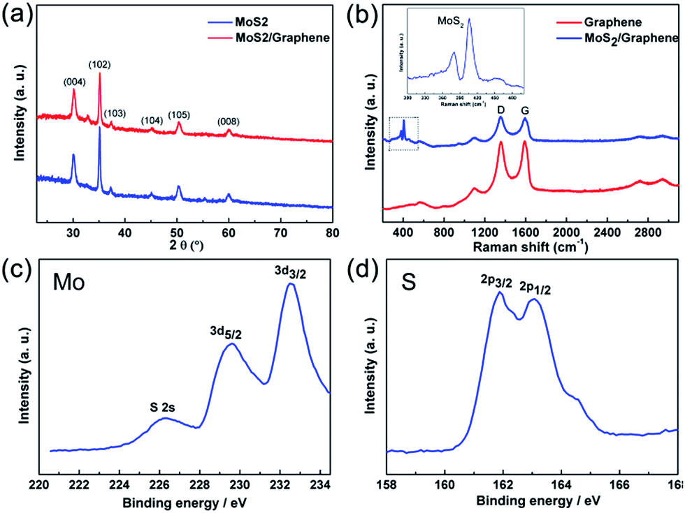 | ||
| Fig. 1 (a) XRD patterns of MoS2 film and MoS2/graphene composite film. (b) Raman spectrum of graphene film and MoS2/graphene composite film. Inset in (b) shows the enlarged MoS2 peaks in the dashed box. (c) and (d) XPS spectra of the MoS2/graphene composite. | ||
In addition, the composite sample was also characterized by X-ray photoelectron spectroscopy (XPS) to verify its chemical composition. Two prominent peaks at 229.6 and 232.6 eV were observed in the Mo3d spectrum in Fig. 1c, which can be attributed to the Mo3d5/2 and Mo3d3/2. Besides, as shown in Fig. 1d, the peaks at 161.9 and 163.1 eV can be ascribed to the spin–orbit couple S2p3/2 and S2p1/2, respectively. These binding energies are all consistent with the reported values for MoS2 crystal.27
Fig. 2 displays the SEM images of the MoS2 and MoS2/graphene composite deposited on FTO substrates at different magnifications. The morphology of pure MoS2 CE shows great difference with that of MoS2/graphene CE. As it can be seen from Fig. 2a and b, the pure MoS2 CE is composed of dense MoS2 nanoparticles and presents relatively smooth surface. This morphology will restrict the reaction area of MoS2 CEs. In contrast, as shown in Fig. 2c, the surface of the MoS2/graphene CE is uneven and exhibits a 3D structure. According to the high-magnification SEM image in Fig. 2d, some MoS2 grown on graphene film shows flake-like structure and this flake-like structure is composed of MoS2 nanoparticles. In addition, we can see that the thickness of graphene is about 180 nm from its cross-section SEM image in Fig. S1.† From Fig. 2e and f, the thickness of pristine MoS2 film and MoS2/graphene composite film also can be estimated to be about 110 nm and 670 nm, respectively. Because graphene thickness remain unchanged (about 180 nm), the grown MoS2 film on graphene is calculated to be 490 nm in thickness, which is much higher than 110 nm of MoS2 film directly grown on FTO. This means that pre-prepared graphene film can promote the growth of MoS2. The as-prepared MoS2/graphene composite shows a 3D morphology, which can obtain a larger surface area as proved in the Fig. S2† and enhance the electrocatalytic activities of the composite when it is used as CE in DSSC. This enlarged surface area of the composite materials was also reported in other articles.33
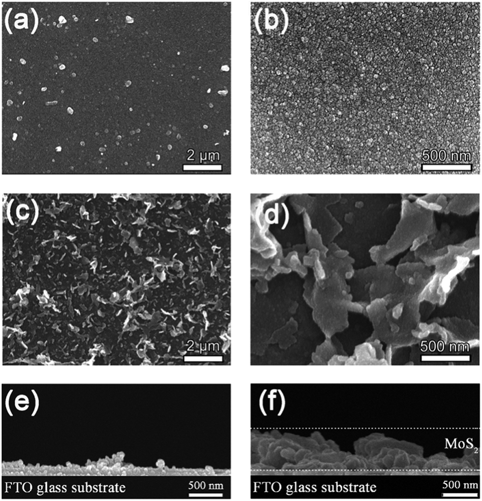 | ||
| Fig. 2 SEM images of (a and b) MoS2 film and (c and d) MoS2/graphene composite film grown on the FTO substrates at different magnifications. (e) and (f) are the cross-section SEM images of MoS2 film and MoS2/graphene composite film, respectively. | ||
The morphology of the MoS2/graphene was further investigated through TEM, as depicted in Fig. 3. Low-magnification TEM image (Fig. 3a) of the as-deposited MoS2/graphene shows uniform MoS2 nanoparticles supported on the surface of graphene films, which agrees with SEM images in Fig. 2d that the flake-like structure is composed of nanoparticles. The inset in Fig. 3a represents SAED pattern of MoS2/graphene and shows the (008), (102), and (107) planes of hexagonal phase MoS2 (JCPDS, PDF no. 77-1716). The result is in coincidence with that of the XRD test. High-resolution TEM image of an individual MoS2 nanoparticle in Fig. 3b shows a lattice spacing of 0.25 nm, which can be ascribed to the (102) planar spacing of MoS2.
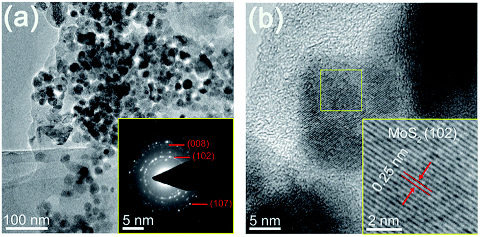 | ||
| Fig. 3 (a) Low-magnification TEM image of as-deposited MoS2/graphene with uniform MoS2 nanoparticles supported on the surface of graphene. The inset in (a) represents SAED pattern of MoS2/graphene and shows the (008), (102), and (107) planes of hexagonal phase MoS2 (JCPDS, PDF no. 77-1716). (b) High-resolution TEM image of an individual MoS2 nanoparticle with the lattice spacing of 0.25 nm in the selected zones marked with yellow frame. | ||
Cyclic voltammetry (CV) was performed to analyze the electrocatalytic abilities of the MoS2, MoS2/graphene (deposition time of graphene is 80 s), and Pt CEs toward the reduction of I3−, which was shown in Fig. 4a. The CV curves of different CEs were scanned from −0.4 V to 1.2 V in ACN solution of 10.0 mM LiI, 1.0 mM I2 and 0.1 M LiClO4, at a scan rate of 50 mV s−1. MoS2/graphene-80 s in the image represents that the deposition time of graphene is 80 s. As shown in Fig. 4a, the CVs of all the three electrodes show two similar pairs of redox peaks (Ox-1/Red-1, Ox-2/Red-2), which indicates that they all have catalytic activities to the reduction of I3−. The Ox-1/Red-1 peaks correspond to the reaction of eqn (1), while the Ox-2/Red-2 peaks correspond to eqn (2).34
| I3− + 2e− ↔ 3I− | (1) |
| 3I2 + 2e− ↔ 2I3− | (2) |
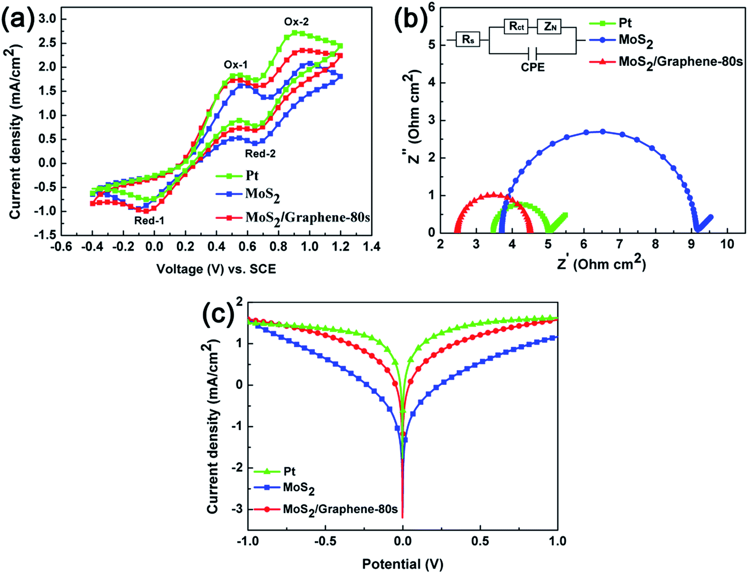 | ||
| Fig. 4 (a) CV curves of the CEs with the films of MoS2, MoS2/graphene (deposition time of graphene is 80 s) and Pt, obtained in ACN solution of 10.0 mM LiI, 1.0 mM I2 and 0.1 M LiClO4, at a scan rate of 50 mV s−1. (b) Nyquist plot and (c) Tafel polarization curves of MoS2, MoS2/graphene and Pt CEs. They were obtained by the use of symmetrical cells and the electrolytes were the same as that used in DSSCs. Inset in (b) shows the equivalent circuit. “MoS2/graphene-80 s” means that the deposition time of graphene is 80 s. | ||
Since the effect of CE in a DSSC is to catalyze the reduction of I3− to I−, the Ox-1/Red-1 peaks should be the main concern of our analysis. The catalytic activities of different CEs can be evaluated from peak current density and the peak-to-peak separation (Epp).35 As displayed in Fig. 4a and Table 1, the Epp of MoS2, MoS2/graphene, and Pt CE is 691 mV, 584 mV, and 572 mV, respectively. It means that the Epp of MoS2/graphene CE is similar to Pt CE and smaller than MoS2 CE, demonstrating that the MoS2/graphene CE has a better reversibility than MoS2 CE. Besides, cathodic peak potential of MoS2 CE (−0.12 V) is smaller than MoS2/graphene CE (−0.05 V), implying I3− is able to be reduced more easily at the interface of MoS2/graphene CEs. Moreover, higher peak current density was achieved for MoS2/graphene CE, further confirming the superior catalytic activities of MoS2/graphene to MoS2 CE. The better electrocatalytic activity of the composite material indicates that this facile all electrochemical strategy is very effective.
| CEs | Voc (V) | Jsc (mA cm−2) | FF (%) | η (%) | Rs (Ω cm2) | Rct (Ω cm2) | Epp (mV) |
|---|---|---|---|---|---|---|---|
| MoS2 | 0.72 | 15.95 | 59.90 | 6.89 | 3.71 | 5.44 | 691 |
| MoS2/graphene-80 s | 0.72 | 16.96 | 65.74 | 8.01 | 2.50 | 1.99 | 584 |
| Pt | 0.73 | 16.86 | 66.72 | 8.21 | 3.45 | 1.56 | 572 |
To further verify the electrocatalytic abilities of different CEs, EIS experiment was studied using symmetric cells, which were fabricated with two identical electrodes and separated by 60 μm thick Surlyn film. Fig. 4b shows the resultant Nyquist plot with the equivalent circuit model in the inset. According to the equivalent circuit, the intercept in high-frequency on the real axis represents the series resistance (Rs) and the left semicircle stands for the charge-transfer resistance (Rct) at the CE/electrolyte interface. The charge-transfer resistance (Rct) can reflect the catalytic activity of different CEs. Z-view software was used to fit the impedance spectra to obtain these parameters, which are shown in Table 1.36
It can be seen in Fig. 4b that the Rs of MoS2/graphene (2.50 Ω cm2) is smaller than that of MoS2 (3.71 Ω cm2), which can be attributed to the superior electrical conductivity of graphene. In addition, the Rct with different CEs is in the order of MoS2 (5.44 Ω cm2) > MoS2/graphene (1.99 Ω cm2) > Pt (1.56 Ω cm2), revealing the facile charge transfer between I3− and MoS2/graphene CE surfaces. Fig. 4c shows the Tafel polarization curves of different CEs carried out using symmetric cells similar to the ones used in EIS. The electrocatalytic activity of CEs is connected with the exchange current density (J0), which can be estimated from the slopes of the anodic or cathodic branches.37 From Fig. 4c, it can be seen that both CEs with Pt and MoS2/graphene have a large J0, while the J0 of MoS2 is smaller than them. It demonstrates that the catalytic activity of MoS2/graphene CE is better than MoS2 CE. This result is in accordance with that of the EIS test. The higher J0 may as a result of the considerable active surface area of the MoS2/graphene CE.
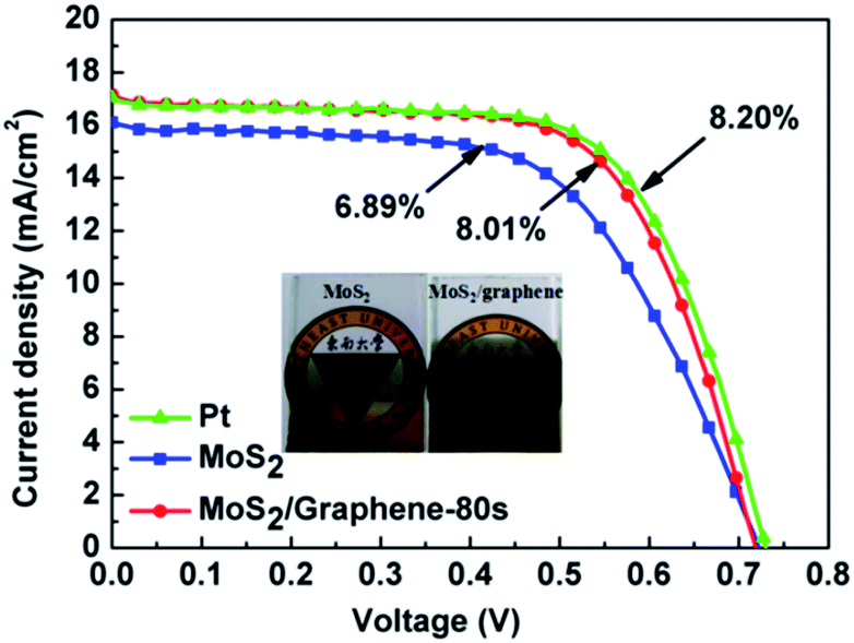
Photocurrent density–voltage (J–V) curves of DSSCs with different CEs were conducted under a simulated solar illumination with a light intensity of 100 mW cm−2, which are shown in Fig. 5. The inset shows the optical photos of MoS2 and MoS2/graphene CEs. The corresponding photovoltaic performance parameters, including the short-circuit photocurrent density (Jsc), open-circuit photovoltage (Voc), fill factor (FF) and cell efficiency of DSSCs are listed in Table 1. It can be seen that the DSSC with graphene/MoS2 CE (deposition time of graphene is 80 s) shows a remarkable cell efficiency of 8.01% (Jsc = 16.96 mA cm−2, Voc = 718 mV, FF = 0.66), while the MoS2 CE-based DSSC exhibits a cell efficiency of 6.89% (Jsc = 15.95 mA cm−2, Voc = 721 mV, FF = 0.59). For comparison, the DSSC with Pt was also measured under the same condition and the cell efficiency of it is about 8.21% (Jsc = 16.86 mA cm−2, Voc = 729 mV, FF = 0.67). Compared to cell with MoS2, the conversion efficiency of the cell with MoS2/graphene was increased by 16.3%, up to 97.6% of the level obtained by using conventional Pt CE. It indicates that the MoS2/graphene CE synthesized by this all electrochemical strategy possesses a good structure, which can improve the cell performance effectively. Both the Jsc and FF are found to increase for the cell with MoS2/graphene, compared to those of the cell with MoS2. The increased Jsc and FF here may be attributed to the good conductivity and the enlarged surface area of the MoS2/graphene CE, which led to a higher cell efficiency.
 | ||
| Fig. 5 Photocurrent density–voltage curves of DSSCs with MoS2 CE, MoS2/graphene CE (deposition time of graphene is 80 s) and Pt CE under a simulated solar illumination with a light intensity of 100 mW cm−2. The inset shows the optical photos of MoS2 and MoS2/graphene CEs. | ||
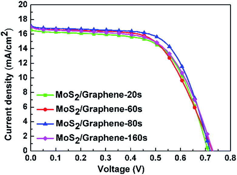
Since the electrochemical deposition of graphene in the CEs can enhance the cell efficiency of DSSCs, the deposition time of the graphene should be a factor that influences the cell performance. So we changed the deposition time of graphene from 20 s to 160 s to analyze the influence of it. The photocurrent density–voltage (J–V) characteristics of MoS2/graphene-based DSSCs with different deposition time of graphene are displayed in Fig. 6 and the corresponding parameters are listed in Table 2. It can be seen that the cell efficiency would not be always enhanced with the increasing deposition time of graphene. When the deposition time of graphene is about 80 s, it would reach an optimal performance of 8.01%. Since the function of graphene is to enhance the conductivity and promote the growth of MoS2 nanoparticles, so the cell performance would be better when graphene is deposited. However, if too much graphene was deposited, the conductivity would be decreased.
 | ||
| Fig. 6 Photocurrent density–voltage curves of the DSSCs based on MoS2/graphene composite CE with different deposition time of graphene. | ||
| CEs | Voc (V) | Jsc (mA cm−2) | FF (%) | η (%) |
|---|---|---|---|---|
| MoS2/graphene-20 s | 0.71 | 16.45 | 63.36 | 7.39 |
| MoS2/graphene-60 s | 0.72 | 16.78 | 61.15 | 7.46 |
| MoS2/graphene-80 s | 0.72 | 16.96 | 65.74 | 8.01 |
| MoS2/graphene-160 s | 0.73 | 16.79 | 61.47 | 7.52 |
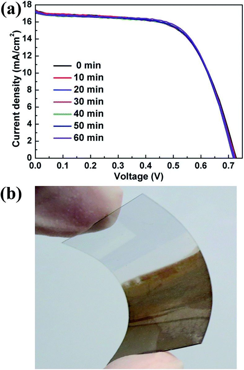
The device stability of the MoS2/graphene based DSSC was examined by repeated J–V measurements at intervals of 10 minutes. As shown in Fig. 7a, there is no obvious change of the curves before and after 1 h illumination. The cell efficiency of the DSSC was 7.82%, 7.84%, 7.85%, 8.00%, 7.91%, 7.98% and 7.99%, respectively. It indicates that the MoS2/graphene CE-based DSSCs have a good stability.
 | ||
| Fig. 7 (a) Stability of the MoS2/graphene based DSSCs. The corresponding photocurrent density–voltage curves were obtained at intervals of 10 minutes. (b) Optical photo of the MoS2/graphene composite deposited on the flexible substrate by this all electrochemical strategy. | ||
To demonstrate whether the MoS2/graphene composite synthesized by this all electrochemical strategy can be tightly adhered to FTO conducting substrate, we used adhesive tape to stick the deposited composite film from FTO. As shown in ESI Movie 1,† almost no material was observed on the adhesive tape, indicating that the proposed all electrochemical strategy can produce stable MoS2/graphene CE film. In addition, this strategy also exhibits its potential in synthesizing graphene-based composite on flexible substrate that cannot withstand high temperature, as we have successfully prepared MoS2/graphene composite on flexible polyethylene terephthalate (PET) substrate coated with ITO by this all electrochemical strategy (Fig. 7b).
Conclusions
In summary, an all electrochemical strategy was used to facilely prepare MoS2/graphene composite films that can directly act as CEs of the DSSCs without needing additional post-treatment. Compared to other strategies that are used to synthesize MoS2/graphene CEs, the fabrication procedures are simplified and the time is markedly reduced by this all electrochemical strategy. Besides, the electrocatalytic ability of MoS2/graphene composite CE is significantly increased compared to that of pure MoS2 CE, because the as-prepared MoS2/graphene composite CE shows a 3D structure, which provides a large surface area. After the optimization, when the deposition time of graphene is 80 s, the cell with MoS2/graphene composite reached a high efficiency of 8.01%, which is comparable to 8.21% of the Pt CE. To the best of our knowledge, it is the first time that this all electrochemical strategy was used in fabricating MoS2/graphene composite CE. Moreover, this all electrochemical strategy also exhibits its potential in synthesizing graphene-based composite on flexible substrate.Acknowledgements
This work was supported by National Basic Research Program of China (973 Program, Grant No. 2015CB352106), National Natural Science Foundation of China (NSFC, Grant No. 61574034, 51372039, 91333118, 61274114, 11525415, 11327901, 11374332 and 51420105003), Jiangsu Province Science and Technology Support Program (Grant No. BK20141118 and BK20151417), and China Postdoctoral Science Foundation Funded Project (Grant No. 2014M550259 and 2015T80480).Notes and references
- B. Oregan and M. Gratzel, Nature, 1991, 353, 737–740 CrossRef CAS
.
- A. Hagfeldt, G. Boschloo, L. C. Sun, L. Kloo and H. Pettersson, Chem. Rev., 2010, 11, 6595–6663 CrossRef PubMed
- F. Xu and L. T. Sun, Energy Environ. Sci., 2011, 4, 818–841 CAS
- Z. Y. Tang, J. H. Wu, M. Zheng, Q. W. Tang, Q. Liu, J. M. Lin and J. L. Wang, RSC Adv., 2012, 2, 4062–4064 RSC
- Z. J. Ning, Y. Fu and H. Tian, Energy Environ. Sci., 2010, 9, 1170–1181 Search PubMed
- M. X. Wu, X. Lin, Y. D. Wang, L. Wang, W. Guo, D. D. Qu, X. J. Peng, A. Hagfeldt, M. Gratzel and T. L. Ma, J. Am. Chem. Soc., 2012, 7, 3419–3428 CrossRef PubMed
- F. Gong, X. Xu, Z. Q. Li, G. Zhou and Z. S. Wang, Chem. Commun., 2013, 14, 1437–1439 RSC
- Y. M. Xiao, G. Y. Han, Y. P. Li, M. Y. Li and Y. Z. Chang, J. Mater. Chem. A, 2014, 10, 3452–3460 Search PubMed
- W. Zhao, X. L. Zhu, H. Bi, H. L. Cui, S. R. Sun and F. Q. Huang, J. Power Sources, 2013, 242, 28–32 CrossRef CAS
- K. S. Lee, W. J. Lee, N. G. Park, S. O. Kim and J. H. Park, Chem. Commun., 2011, 14, 4264–4266 RSC
- C. Y. Zhu, F. Xu, J. Chen, H. H. Min, H. Dong, L. Tong, K. Qasim, S. L. Li and L. T. Sun, J. Power Sources, 2016, 303, 159–167 CrossRef CAS
- Z. Y. Zhang, S. P. Pang, H. X. Xu, Z. Z. Yang, X. Y. Zhang, Z. H. Liu, X. G. Wang, X. H. Zhou, S. M. Dong, X. Chen, L. Gu and G. L. Cui, RSC Adv., 2013, 3, 16528–16533 RSC
- J. S. Jang, D. J. Ham, E. Ramasamy, J. Lee and J. S. Lee, Chem. Commun., 2010, 45, 8600–8602 RSC
- M. Al-Mamun, H. Zhang, P. Liu, Y. Wang, J. Caoac and H. J. Zhao, RSC Adv., 2014, 4, 21277–21283 RSC
- S. J. Peng, P. N. Zhu, Y. Z. Wu, S. G. Mhaisalkara and S. Ramakrishna, RSC Adv., 2012, 2, 652–657 RSC
- Z. B. Yang, T. Chen, R. X. He, H. P. Li, H. J. Lin, L. Li, G. F. Zou, Q. X. Jia and H. S. Peng, Polym. Chem., 2013, 4, 1680–1684 RSC
- X. N. Zhang, J. Zhang, Y. Z. Cui, J. W. Feng and Y. J. Zhu, J. Appl. Polym. Sci., 2013, 1, 75–79 CrossRef
- M. H. Yeh, L. Y. Lin, C. Lee, H. Y. Wei, C. Y. Chen, C. G. Wu, R. Vittal and K. C. Ho, J. Mater. Chem., 2011, 47, 19021–19029 RSC
- H. Y. Cai, Q. W. Tang, B. L. He and P. J. Li, J. Power Sources, 2014, 258, 117–121 CrossRef CAS
- J. Y. Lin, J. H. Liao and T. Y. Hung, Electrochem. Commun., 2011, 9, 977–980 CrossRef
- S. Y. Tai, C. J. Liu, S. W. Chou, F. F. S. Chien, J. Y. Lin and T. W. Lin, J. Mater. Chem., 2012, 47, 24753–24759 RSC
- J. Zhang, S. Najmaei, H. Lin and J. Lou, Nanoscale, 2014, 10, 5279–5283 RSC
- C. X. Guo, H. B. Yang, Z. M. Sheng, Z. S. Lu, Q. L. Song and C. M. Li, Angew. Chem., Int. Ed., 2010, 49, 3014–3017 CrossRef CAS PubMed
- C. X. Guo, G. H. Guai and C. M. Li, Adv. Energy Mater., 2011, 1, 448–452 CrossRef CAS
- H. Choi, H. Kim, S. H. Wang, Y. Han and M. Jeon, J. Mater. Chem., 2011, 21, 7548–7551 RSC
- H. Wang and Y. H. Hu, Energy Environ. Sci., 2012, 8, 8182–8188 Search PubMed
- C. J. Liu, S. Y. Tai, S. W. Chou, Y. C. Yu, K. D. Chang, S. Wang, F. S. S. Chien, J. Y. Lin and T. W. Lin, J. Mater. Chem., 2012, 22, 21057–21064 RSC
- J. Y. Lin, C. Y. Chan and S. W. Chou, Chem. Commun., 2013, 49, 1440–1442 RSC
- G. Yue, J. Y. Lin, S. Y. Tai, Y. M. Xiao and J. H. Wu, Electrochim. Acta, 2012, 85, 162–168 CrossRef CAS
- H. C. Bi, K. B. Yin, X. Xie, Y. L. Zhou, N. Wan, F. Xu, F. Banhart, L. T. Sun and R. S. Ruoff, Adv. Mater., 2012, 24, 5124–5129 CrossRef CAS PubMed
- Y. G. Zhou, J. J. Chen, F. B. Wang, Z. H. Sheng and X. H. Xia, Chem. Commun., 2010, 46, 5951–5953 RSC
- G. L. Frey, R. Tenne, M. J. Matthews, M. S. Dresselhaus and G. Dresselhaus, Phys. Rev. B: Condens. Matter Mater. Phys., 1999, 4, 2883–2892 CrossRef
- S. L. Yang, Y. W. Huang, W. Zhu, B. C. Deng, H. Wang, Z. H. Zhang, P. F. Bao and G. Z. Wang, Int. J. Hydrogen Energy, 2014, 39, 15063–15071 CrossRef CAS
- P. P. Sun, F. Yao, X. Y. Ban, N. Huang and X. H. Sun, Electrochim. Acta, 2015, 174, 127–132 CrossRef CAS
- F. Gong, H. Wang, X. Xu, G. Zhou and Z. S. Wang, J. Am. Chem. Soc., 2012, 26, 10953–10958 CrossRef PubMed
- C. Y. Zhu, H. H. Min, F. Xu, J. Chen, H. Dong, L. Tong, Y. M. Zhu and L. T. Sun, RSC Adv., 2015, 5, 85822–85830 RSC
- C. W. Kung, H. W. Chen, C. Y. Lin, K. C. Huang, R. Vittal and K. C. Ho, ACS Nano, 2012, 8, 7016–7025 CrossRef PubMed
Footnotes |
| † Electronic supplementary information (ESI) available. See DOI: 10.1039/c6ra02494g |
| ‡ These authors contributed equally. |
| This journal is © The Royal Society of Chemistry 2016 |