
Ge-alloyed CZTSe thin film solar cell using molecular precursor adopting spray pyrolysis approach†
Dhruba B. Khadka‡
,
SeongYeon Kim and
JunHo Kim*
Department of Physics, Incheon National University, 12-1 Songdo-dong Yeonsu-gu, 406-772 Incheon, South Korea. E-mail: jhk@inu.ac.kr; Tel: +82-32-835-8221
First published on 30th March 2016
Abstract
We report a promising fabrication approach for the synthesis of Ge-alloyed Cu2Zn(GexSn1−x)Se4 (CZGTSe) thin films using molecular precursors by spray pyrolysis to obtain band gap tuned kesterite solar cells. A stable and well dissolved precursor solution of CZTS/CZGTS with the desired elemental composition is prepared in DMSO solvent, sprayed on a Mo substrate and subsequently selenized under ambient selenium at high temperature to obtain well-crystallized absorber layers. The Ge-alloyed CZTSe thin films had improved surface morphology, grain size and crystal quality, which led to power conversion efficiencies as high as 4.72%. The growth properties and device analysis suggest that enhancement of the device performance can be achieved by further optimization of the absorber and interface layers with mitigation of defect activities.
1. Introduction
Kesterite material Cu2ZnSnS(Se)4 (CZTSSe) based thin film solar cells have emerged as promising candidates for scalable photovoltaic technology because of their earth-abundant, low-toxicity constituents and desirable optoelectronic properties.1–3 Device efficiencies up to 12.6% have been achieved using CZTSSe absorber layers with Se-rich stoichiometry processed from hydrazine based precursor solutions.3 This record performance is much lower than the estimated theoretical efficiency (∼31%) of CZTSSe thin film solar cells.2 A band gap tuning/grading approach using kesterite CZTSSe can be utilized to enhance the device performance, adopting a similar approach to that of high-efficiency band graded CIGSe thin film solar cells.4 Some reports on alloyed CZTSSe absorber materials have shown effective band gap tunability by substitution of Sn with Ge and substitution of Zn with Fe in the CZTSSe crystal lattice without controlling the anion (S/Se) ratio.5–10 Since Ge-alloyed CZTSSe solar cells have demonstrated improvements in device performance, the Ge substitution approach is receiving much focus to deepen the understanding of the structural and optoelectronic properties of the cells.11–14 Additionally, the incorporation of stable Ge atoms in the CZTSSe crystal lattice may minimize the formation of deep defects associated with multivalent Sn atoms and is hence beneficial to improve the quality of absorber materials.7,13,14 In recent progress, Ge alloyed CZTSSe solar cell devices have been reported with efficiencies up to 9.4% using nanocrystal ink of Cu2Zn(GexSn1−x)S4 (CZGTS) with 30% Ge content.11 Bag et al. also achieved a slight enhancement in device efficiency, as high as 9.14%, for Ge substituted CZTSe solar cells fabricated by adopting a hydrazine based precursor approach.13 Similarly, solar cells with band graded CZTS absorber layers with varying Ge content have demonstrated improvements in device efficiency from 4.6% to 6% by adopting a solution approach.12 Moreover, CZTSe solar cells fabricated from sputtered stacked CZTS introducing a superficial very thin Ge metallic layer have shown a device enhancement of 3% compared to pure CZTSe solar cells.15,16 Earlier reports on Ge alloyed CZTSe solar cell devices indicate that there is a need for systematic investigation of various aspects of the fabrication techniques, control of absorber layer quality, and interface optimization to achieve solar cell devices as efficient as band graded CIGSe technology.From a cost perspective, non-vacuum techniques are highly advantageous for the fabrication of thin film solar cells; hence, various solution process techniques, including spin coating, doctor blading, spray pyrolysis and electrodeposition, have been widely employed for the fabrication of kesterite based thin film solar cells.3,11,17–19 Many solution approaches with liquid coatings, nanocrystal/nanoparticle inks and molecular ink precursors with various solvents have been used to prepare kesterite absorber layers.18,19 Among the abovementioned techniques, the fabrication of kesterite absorber layers using molecular ink precursor prepared with nontoxic solvent, especially avoiding hydrazine and high carbon organic solvents, is the most promising due to low toxicity, safety, and easy control of the precursor concentration/cation stoichiometry of the absorber layer.20 Recently, some research groups reported CZTSSe solar cells fabricated using molecular precursor ink prepared in water and dimethyl sulfoxide (DMSO) solvent whose device efficiencies are competitive with the highest efficiencies reported to date.21–24 It is to be noted that there are few reports about Ge alloyed CZTSSe solar cells using either vacuum or non-vacuum approaches. Band graded CZTSSe absorber layers with varying ratios of Sn/Ge can be experimentally realized if the elemental loss of Sn or Ge is well controlled during crystallization under high temperature annealing. Although Ge alloyed CZTSSe solar cells using hydrazine based precursors and nanocrystal ink were successfully fabricated by adopting a solution approach, there are still few extensive studies of the fabrication of Ge alloyed CZTSSe solar cells using various fabrication techniques with different molecular precursors.
Here, we studied the fabrication of CZTSe and Ge-alloyed CZTSe (CZGTSe) thin film solar cells with a Cd-free In2S3 buffer layer, adopting a solution based approach by chemical spray pyrolysis (CSP). CSP is simple, cost effective and enables easy control of the stoichiometry by varying the precursor composition. Our group has previously reported the study of kesterite materials for photovoltaic applications fabricated by the CSP technique.5,9,19,25,26 In this work, CZTSe and CZGTSe absorber layers were fabricated by a spray pyrolysis approach using a molecular precursor solution prepared with DMSO solvent. In our experience, the precursor solution of CZGTS prepared in DMSO solvent was found to demonstrate good solubility and stability compared to aqueous precursor solution, as depicted in Fig. S1 (ESI†). Thus, we switched to precursor solution prepared in DMSO solvent, which is preferable.20,23 A power conversion efficiency as high as 4.74% was demonstrated for a thin film solar cell device with a CZGTSe absorber layer fabricated by spray pyrolysis using a molecular precursor of CZGTS prepared with DMSO solvent for the first time. We report a comparative study on the material growth properties of CZTSe and CZGTSe absorber layers as well as the characterization of the fabricated devices.
2. Experimental details
2.1. Materials
Copper(II) acetate monohydrate (Cu(CH3COO)2; ≥99%), zinc chloride (ZnCl2; ≥98%), tin(IV) chloride pentahydrate (SnCl4·5H2O; 98%), germanium chloride (GeCl4; ≥98%), germanium iodide (GeI4; ≥98%), indium chloride (InCl3; 98%), thiourea (SC(NH2)2; ≥99.0%), elemental selenium powder (99.99%, diameter: 75 μm), and dimethyl sulfoxide (DMSO) ((CH3)2SO; ≥98%) were used as received from Sigma-Aldrich.2.2. Preparation of CZTSe and CZGTSe thin films
The CZTSe and CZGTSe absorber layers were prepared by selenization of the respective as-sprayed CZTS thin films deposited on Mo-coated soda lime glass (Mo-SLG) substrate by CSP. For deposition of the thin films, the precursor solution was prepared with copper(II) acetate monohydrate, zinc chloride, tin(IV) chloride pentahydrate, germanium iodide and thiourea, which were completely dissolved in DMSO solvent by magnetic stirring and diluted by one fourth of the volume with ethanol. The precursor solutions were prepared for deposition with a molar ratio of Cu(CH3COO)2![[thin space (1/6-em)]](https://www.rsc.org/images/entities/char_2009.gif) :ZnCl2:SnCl4·5H2O:SC(NH2)2 = 1.85:1.2:1:10 for the as-sprayed CZTS thin films and prepared as Cu:Zn:Ge:Sn:S = 1.85:1.2:0.3:0.7:10 for the as-sprayed CZGTS thin films. In our earlier reports on various kesterite materials, the precursor solution was prepared with de-ionized water (DIW).5,9,25 Although we also attempted to prepare sprayed thin films with CZGTS precursor solutions using germanium chloride, germanium oxide and germanium iodide in DIW solvent, the precursor solution with germanium iodide was found to be superior due to good solubility and a lack of powdery film formation. However, we experienced difficulty in preparing a well-dissolved and stable solution of CZGTS precursor with DIW solvent. Thus, to overcome this difficulty, the precursor solution was prepared with DMSO solvent. It is notable that both precursor solutions for CZTS and CZGTS prepared in DMSO solvent were found to be well dissolved and stable for longer times. A well-dissolved precursor solution in DMSO is highly preferable to obtain better quality as-deposited thin films. The prepared precursor solution was deposited onto Mo-SLG at a substrate temperature of 450 °C using a homemade electrostatic field assisted ultrasonic spray system. The molecular mist of CZGTS (CZTS) precursor solution was transferred with a flow of N2 gas. We set the flow rate as 2 lpm and a high electrostatic field between the transfer tube and the substrate,5,9,25 which provided a precursor transfer rate of ∼0.3 ml min−1 and resulted in a deposition rate of the as-sprayed film of ∼100 nm min−1. The as-sprayed films were selenized by rapid thermal annealing with a heating rate of 50 °C min−1 under ambient selenium vapor and were maintained at ∼500 to 520 °C for 30 min inside a rectangular graphite box filled with selenium powder (99.99%) to obtain well-crystallized absorber layers. The schematics of the crystallization temperature profile and the furnace for selenization can be found in our earlier reports.9,26
:ZnCl2:SnCl4·5H2O:SC(NH2)2 = 1.85:1.2:1:10 for the as-sprayed CZTS thin films and prepared as Cu:Zn:Ge:Sn:S = 1.85:1.2:0.3:0.7:10 for the as-sprayed CZGTS thin films. In our earlier reports on various kesterite materials, the precursor solution was prepared with de-ionized water (DIW).5,9,25 Although we also attempted to prepare sprayed thin films with CZGTS precursor solutions using germanium chloride, germanium oxide and germanium iodide in DIW solvent, the precursor solution with germanium iodide was found to be superior due to good solubility and a lack of powdery film formation. However, we experienced difficulty in preparing a well-dissolved and stable solution of CZGTS precursor with DIW solvent. Thus, to overcome this difficulty, the precursor solution was prepared with DMSO solvent. It is notable that both precursor solutions for CZTS and CZGTS prepared in DMSO solvent were found to be well dissolved and stable for longer times. A well-dissolved precursor solution in DMSO is highly preferable to obtain better quality as-deposited thin films. The prepared precursor solution was deposited onto Mo-SLG at a substrate temperature of 450 °C using a homemade electrostatic field assisted ultrasonic spray system. The molecular mist of CZGTS (CZTS) precursor solution was transferred with a flow of N2 gas. We set the flow rate as 2 lpm and a high electrostatic field between the transfer tube and the substrate,5,9,25 which provided a precursor transfer rate of ∼0.3 ml min−1 and resulted in a deposition rate of the as-sprayed film of ∼100 nm min−1. The as-sprayed films were selenized by rapid thermal annealing with a heating rate of 50 °C min−1 under ambient selenium vapor and were maintained at ∼500 to 520 °C for 30 min inside a rectangular graphite box filled with selenium powder (99.99%) to obtain well-crystallized absorber layers. The schematics of the crystallization temperature profile and the furnace for selenization can be found in our earlier reports.9,26
2.3. Device fabrication
The device structures were constructed by subsequent deposition of an In2S3 buffer layer by spray pyrolysis and ZnO/ITO as the window layer by the rf-sputtering method.16 For the deposition of indium sulfide buffer, a precursor solution prepared by dissolving InCl3 and SC(NH2)2 with a molar ratio of 1:7 in water–ethanol solvent was sprayed onto a post-selenized CZGTSe (CZTSe) absorber layer, as described in earlier reports.16,19 Chemical etching in 10% of aqueous solution of potassium cyanide (KCN) proceeded on the surface of each absorber layer for 3 minutes prior to buffer deposition. Finally, the kesterite solar cell devices were completed by subsequent deposition of an intrinsic zinc oxide (i-ZnO) layer and an indium tin oxide (ITO) layer by rf magnetron sputtering.
2.4. Film and device characterization
The composition, surface morphology and cross-sectional image of the samples were studied using a field emission scanning electron microscope (FESEM, JEOL, JSM-7001F) equipped for energy dispersive X-ray spectroscopy (EDS, Oxford, INCA). The crystal structure and phase were investigated by X-ray diffraction (XRD) and Raman spectroscopy. The XRD patterns were obtained in 2θ scans at a scanning rate of 3° per min using an XRD system (Rigaku, Smart Lab) equipped with a Cu Kα source of λ = 1.5412 Å operated at 45 kV and 200 mA. The Raman spectroscopy measurements were conducted using a Spectro Raman system equipped with a spectrometer (Mmac 750) and a laser with an excitation wavelength of λ = 532 nm (irradiation power, <1 mW) and a spot size of approximately 1 μm. To investigate the electrical properties of the absorber layer, we carried out Hall effect measurements. The Hall effect measurements were performed using a Hall effect measurement system (HMS-3000, Ecopia) and the Van der Pauw method under an applied magnetic field of 0.55 T. The fabricated CZTSe solar cell device was characterized by current density–voltage (J–V) measurements, external quantum efficiency (EQE) and admittance spectroscopy (AS). The J–V measurements were performed with a source meter (Keithley 2400) and under AM 1.5G filtered illumination of a 1000 W m−2 Xe lamp (Abet Technology), which has been calibrated with a Si reference solar cell. The quantum efficiency measurements were carried out with a Xe light source, a monochromator combined with a light chopper and a lock-in amplifier system (Mc Science).3. Results and discussion
3.1. Crystal structure and electrical properties
The crystal structure and quality of the as-sprayed and post-selenized thin films were characterized by XRD and Raman spectroscopy measurements. The XRD patterns and Raman spectra of the as-sprayed films (Fig. S2, ESI†) indicate poor crystal quality. Here, the post-selenized CZTSe and CZGTSe thin film absorber layers (Fig. 1a) show well-crystallized XRD patterns with sharp, dominant diffraction peaks with (112) orientation and other small peaks of the (101), (200), (004), (220), (204), (312), (116) and (314) planes, assigned to the kesterite structure.5,6,13,14 The crystal lattice parameters calculated from the XRD patterns of the respective films (Fig. 1a) are listed in Table S1 (ESI†). The dominant XRD peak was found to be shifted to a higher 2θ angle for the CZGTSe thin film due to a decrease in unit cell volume (Table S1†) as a consequence of incorporation of Ge in the CZTSe lattice in place of the Sn atom, which has a large atomic radius; this is close agreement with previous reports.5,13,14 To obtain further confirmation of the crystal quality, the XRD results were coupled with the Raman spectra of the respective films, as exhibited in Fig. 1b. The CZTSe thin film assigns a dominant characteristic peak at 195 cm−1 with small peaks at 172 and 232 cm−1, whereas the CZGTSe film exhibits a main peak at 198 cm−1 along with other characteristic peaks at 174 and 235 cm−1 of the kesterite phase, showing the blue shifting trend observed in the XRD patterns (Fig. 1a) as a consequence of Ge alloying, which is consistent with earlier reports.5,6,11 Although there are no noticeable characteristic peaks attributable to possible secondary phase,5,27 further study of the films with resonant Raman scattering is required for precise confirmation.28,29 From the results of the XRD and Raman measurements (Fig. 1a and (b)) and crystal structure analysis, it appears that the post-selenized CZTSe and CZGTSe thin films are well crystallized, with a dominant kesterite phase. | ||
| Fig. 1 X-ray diffraction patterns (a) and Raman spectra (b) of post-selenized CZTSe and CZGTSe thin film absorber layers. The shifting of the characteristic peaks of XRD to higher 2θ degrees and the blue shifting of Raman peaks is due to unit cell contraction with the replacement of Sn by smaller atomic sized Ge. | ||
The basic electrical properties of the fabricated films obtained from Hall measurements are summarized in Table S2 (ESI†). The electrical parameters of carrier concentration, mobility, and resistivity of the CZTSe film are measured to be 5.946 × 1017 cm−3, 9.656 × 10⁻¹ cm2 V−1 s−1, and 1.087 × 101 Ω cm, respectively, whereas those for CZGTSe film are measured to be 5.242 × 1018 cm−3, 1.982 cm2 V−1 s−1, and 1.664 Ω cm, respectively. These results indicate that Ge-alloying results in a slight improvement to the electrical properties of the absorber layer.
3.2. Film composition and crystal growth
The surface morphology and elemental composition of the as-sprayed and post-selenized CZTSe and CZGTSe films were studied by SEM and EDS. The surface textures of the respective films are depicted in Fig. 2. Both of the as-sprayed films (Fig. 2(a) and (c)) show poor surface texture, whereas the respective post-selenized films (Fig. 2(b) and (d)) reveal good crystallization, with clear and enhanced grains. The grain size of the Ge alloyed CZTSe thin film was found to be larger than that of the CZTSe thin film, as others have reported.5,6,16 The EDS results of the as-sprayed films have elemental compositional ratios of Cu/(Zn + Sn) = 0.85, Zn/Sn = 1.2, S/(Cu + Zn + Sn) = 0.85 and Ge/(Sn + Ge) = 0.28 with the presence of a significant proportion of oxygen element. This oxygen content is usually observed in as-sprayed films because these films were prepared by deposition in ambient air at elevated temperature; this is believed to be a contributing factor for poor crystal quality, as revealed by the XRD patterns and Raman spectroscopy results (Fig. S2, ESI†). The elemental compositions of the post-selenized CZTSe and CZGTSe thin films estimated from the EDS results were found to be Cu/(Zn + Sn) = 0.79, Zn/Sn = 1.17, Se/(Cu + Zn + Sn) = 1.19 and S/(S + Se) = 0.06 for the CZTSe thin film (Fig. 2c) and Cu/(Zn + Sn + Ge) = 0.82, Zn/(Sn + Ge) = 1.18, Ge/(Ge + Sn) = 0.24, Se/(Cu + Zn + Sn) = 1.22 and S/(S + Se) = 0.058 for the CZGTSe thin film (Fig. 2d). The oxygen contents in the post-selenized films were observed to be so drastically reduced as to be negligible (for example, O/(O + S + Se) < 0.05 for the air exposed sample). The error of EDS measurement is ±5% that of the measured value of the atomic weight percentage. The SEM results indicate that the as-sprayed films are well crystallized after selenization to form CZTSe and CZGTSe thin film absorber layers; this is strongly supported by the XRD and Raman results, as depicted in Fig. 1. Moreover, a slight Ge loss was observed in the post-selenized CZGTSe thin film, which was also reported in other reports on Ge-alloyed CZTSe material.11,30 | ||
| Fig. 2 SEM images of as-sprayed CZTS (a) and CZGTS (c) thin films and postselenized CZTSe (b) and CZGTSe (d). | ||
The cross-sectional images of kesterite solar cell devices consisting of CZTSe and CZGTSe absorber layers are depicted in Fig. 3. The complete solar cell devices (Fig. 3) consist of multilayers: a transparent conducting oxide (TCO) layer of ITO (∼250 nm)/i-ZnO (∼70 nm)/a buffer layer of In2S3 (∼100 nm)/an absorber layer of CZTSe (∼0.9 μm) or CZGTSe (∼0.8 μm)/a back contact layer of MoSe2/Mo (∼0.6 μm)/SLG. The solar cell cross-section showed well-crystallized absorber layers of cross-sectional images with thicknesses of about 0.8 μm, composed of large grains. The cross-sectional images depict well buried In2S3 buffer layers in both devices and a thin interface layer of MoSe2 between the back contact Mo layer and the respective absorber layers which formed during the selenization. The cross-sectional image of the CZTSe solar cell (Fig. 3a) showed some voids and small features at the bottom of the absorber layer, which are reported to act as recombination centers,11,12,14 whereas these features were not as apparent in the cross-sectional image of the CZGTSe solar cell (Fig. 3b); this demonstrates the beneficial aspects of Ge alloying. Thus, the surface texture and cross-sectional features of the Ge-alloyed CZTSe thin film solar cells can be further improved by optimizing the absorber layer growth conditions and interface layer quality.
 | ||
| Fig. 3 Cross-sectional SEM images of the solar cell devices, consisting of SLG/Mo/MoSe2/kesterite absorber/In2S3/ZnO/ITO. Here, CZTSe (a) and CZGTSe (b) have been used as kesterite absorbers. | ||
3.3. Device characteristics
The J–V characteristics of the best devices, as shown in Fig. 4a, demonstrate a device efficiency of 3.82% for the CZTSe thin film solar cell, which is enhanced to 4.72% for the CZGTSe thin film solar cell with Ge alloying, showing improvement in the device parameters of open circuit voltage (VOC) and fill factor (FF), as given in the tabulated inset in Fig. 4a. The improvement in the device parameters is closely associated with the improved quality of the CZGTSe absorber layer, as discussed earlier. The performances of these devices fabricated by adopting spraying deposition with DMSO precursor solutions exhibited promising results. There is much room to improve the device parameters after further optimization of the absorber layer and interface layer quality.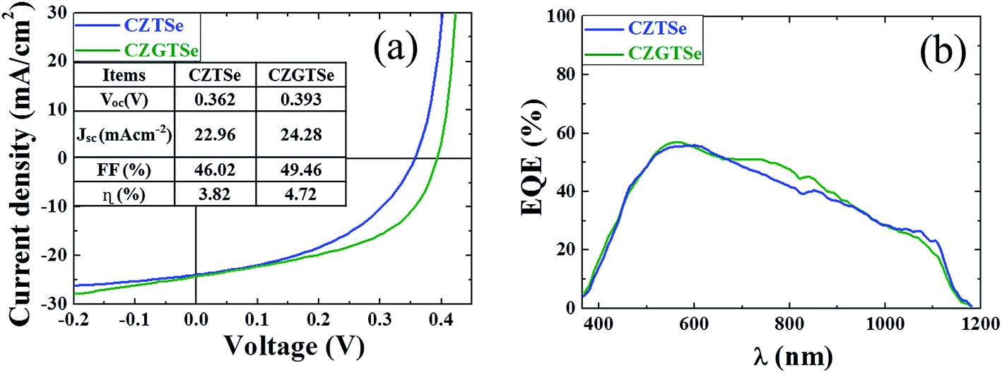 | ||
| Fig. 4 J–V characteristics of CZTSe and CZGTSe solar cells (a). External quantum efficiency (EQE) of respective devices (b). The inset table in (a) summarizes the device parameters of solar cell devices having an area of ∼0.1 cm2. | ||
Fig. 4b depicts the external quantum efficiency (EQE) of the best solar cell device, with J–V characteristics (Fig. 4a). There is a less noticeable enhancement of the spectral response, which is consistent with the short circuit current (JSC) values of the respective device. Although the maximum EQE (∼60%) for both devices corresponds to around 570 nm, there is a slightly higher EQE value in the buffer response (short wavelength) regime and the absorber response (longer wavelength) regime,31–33 which indicates the effect of the slight increment in band gap energy and the better crystal quality of the Ge alloyed absorber layer. The slanting decrease in EQE response in the longer wavelength regime (600 to 1150 nm) indicates the loss of deeply absorbed photons due to recombination in the bulk and depletion regions and reflection loss from the solar cell surface. The EQE results show slight band tailing, which is ascribed to defect complexes in the absorber layer.33–35 The band gap estimations of the respective devices from the EQE responses were found to be approximately 1.09 and 1.13 eV for the CZTSe and CZGTSe absorber layers, as shown in Fig. S3 (ESI†). These estimated values of Eg are found to be somewhat consistent with the Ge alloying effect in the CZTSe absorber layer.
To obtain further information about the electrical parameters, we also analyzed the J–V curves of the devices, adopting approaches outlined in previous reports.32 Fig. 5(a)–(c) shows the plots for the estimation of series resistance (Rs), the diode ideality factor (A) and the reverse saturation current density (J0). The Rs value, 0.532 Ω cm2 for the CZTSe solar cell, is higher than the Rs value of 0.191 Ω cm2 for the CZGTSe solar cell, as depicted in Fig. 5b. Similarly, the value of J0 is found to be decreased from 7.02 × 10⁻⁵ A cm−2 (for CZTSe) to 5.59 × 10⁻⁶ A cm−2 (for CZGTSe), as given in Fig. 5c. The higher value of J0 is caused by the higher defect activities, which is associated with the limitation of VOC as well as of FF.2,34 Here, the lower value of J0 for the CZGTSe solar cell device compared to that of the CZTSe device indicates that the increase in VOC and FF might be associated with the minimization of defect activities as a consequence of the improvement in the crystal quality by Ge alloying. However, the estimated values of J0 are much higher than the reported value (10−9 A cm−2) for high efficiency devices,34,36 which indicates that there is a need to control the defect activity to enhance the device efficiency by improving the device parameters (especially VOC and FF). In addition, the diode ideality factor (A) was found to decrease from an average of ∼2.68 to ∼1.87 for the CZGTSe device, as shown in Fig. 5c. This result is consistent with the value of the reverse saturation current, since the value of A is also associated with the recombination mechanism. It is reported that if the value of A is close to but ≤2, it is believed to have Shockley–Read–Hall (SRH) recombination in the space charge region (SCR), while if the value of A is higher than 2, the defect activities are believed to be governed by a complex recombination process with traps distributed in the interface, surface and carrier tunneling.35–38 In the case of our devices, since the value of A (∼2.68) is higher than 2, the CZTSe device may have suffered from complex recombination phenomena, whereas the decrease in value of A (1.87) indicates the alleviation of defect activities in the CZGTSe device. Thus, the results of the electrical parameters extracted from the J–V curve analysis collectively corroborate the facts that the improvement in device performance of the CZGTSe solar cell is attributed to the alleviation of complex defect activities by Ge alloying in the CZTSe absorber layer.
 | ||
| Fig. 5 J–V analysis of CZTSe and CZGTSe solar cell devices, adopting the one-diode model. | ||
Some issues could be addressed to improve the device performance of the Ge-alloyed CZTSe solar cell by a spray pyrolysis approach using molecular precursor prepared with DMSO solvent. As discussed above, there is a deficit in VOC (Eg − VOC) of more than 0.7 V, which is much higher than other reports;39,40 this reveals the existence of significant recombination centers either in the bulk absorber layer or at the interfaces, such as the buffer/absorber and back contact (Mo)/absorber interfaces.34,36,40 The remedy of this voltage deficit could be an important breakthrough for kesterite based thin film solar cells. These limitations can be addressed by improving the absorber and interface layer quality and the fine tuning of the band gap energy with proper Ge alloying, or band graded absorber layers with varying Ge content can be employed to achieve efficient light harvesting to enhance the device performance.
4. Conclusions
We report the fabrication of kesterite based thin film solar cells by adopting a chemical spray pyrolysis technique using stable and well-dissolved precursor solution prepared in DMSO solvent. The kesterite CZTSe and CZGTSe absorber layers were prepared by spraying DMSO based molecular precursor solution followed by selenization at high temperature under ambient selenium vapor. The surface morphology and crystal quality of the absorber layers were found to improve with Ge alloying in the CZTSe thin film. The solar cells demonstrated enhancements in their device efficiencies of 3.82% for CZTSe to 4.72% for CZGTSe absorber layers with In2S3 buffer deposited by the spray route. The analysis of the electrical properties showed high reverse saturation current and voltage deficit, which are attributed to complex defect activities which can be improved by optimization of the absorber and interface layers. This report presents the feasibility of band gap tuning of CZGTSe absorber layers for photovoltaic applications by adopting a simple solution approach for spray pyrolysis.Acknowledgements
This research work was financially supported by the National Research Foundation of Korea (NRF) funded by the Korean government (NRF-2014R1A2A1A11053109) and the New & Renewable Energy of the Korea Institute of Energy Technology Evaluation and Planning (KETEP) grant funded by the Korea government and Ministry of Trade, Industry and Energy (No. 20123010010130).References
- D. B. Mitzi, O. Gunawan, T. K. Todorov and D. A. R. Barkhouse, Philos. Trans. R. Soc., A, 2013, 371, 20110432 CrossRef PubMed.
- S. Siebentritt, Thin Solid Films, 2013, 535, 1–4 CrossRef CAS.
- W. Wang, M. T. Winkler, O. Gunawan, T. Gokmen, T. K. Todorov, Y. Zhu and D. B. Mitzi, Adv. Energy Mater., 2014, 4, 13014651–13014655 Search PubMed.
- A. Chirila, S. Buecheler, F. Pianezzi, P. Bloesch, C. Gretener, A. R. Uhl, C. Fella, L. Kranz, J. Perrenoud, S. Seyrling, R. Verma, S. Nishiwaki, Y. E. Romanyuk, G. Bilger and A. N. Tiwari, Nat. Mater., 2011, 10, 857–861 CrossRef CAS PubMed.
- D. B. Khadka and J. H. Kim, J. Phys. Chem. C, 2015, 119, 1706–17013 CAS.
- A. S. R. Chesman, J. Embden, E. D. Gaspera, N. W. Duffy, N. A. S. Webster and J. J. Jasieniak, Chem. Mater., 2014, 26, 5482–5491 CrossRef CAS.
- Q. Shu, J. H. Yang, S. Chen, B. Huang, H. Xiang, X. G. Gong and S. H. Wei, Phys. Rev. B: Condens. Matter Mater. Phys., 2013, 87, 1152081–1152085 Search PubMed.
- G. M. Ford, Q. Guo, R. Agrawal and H. W. Hillhouse, Chem. Mater., 2011, 23, 2626–2629 CrossRef CAS.
- D. B. Khadka and J. H. Kim, J. Phys. Chem. C, 2014, 118, 14227–14237 CAS.
- T. Shibuya, Y. Goto, Y. Kamihara, M. Matoba, K. Yasuoka, L. A. Burton and A. Walsh, Appl. Phys. Lett., 2014, 104, 0219121–0219124 CrossRef.
- C. J. Hages, S. Levcenco, C. K. Miskin, J. H. Alsmeier, D. Abou-Ras, R. G. Wilks, M. Bar, T. Unold and R. Agrawal, Prog. Photovoltaics, 2015, 23, 376–384 CAS.
- I. Kim, K. Kim, Y. Oh, K. Woo, G. Cao, S. Jeong and J. Moon, Chem. Mater., 2014, 26, 3957–3965 CrossRef CAS.
- S. Bag, O. Gunawan, T. Gokmen, Y. Zhu and D. B. Mitzi, Chem. Mater., 2012, 24, 4588–4593 CrossRef CAS.
- Q. Guo, G. M. Ford, W. C. Yang, C. J. Hages, H. W. Hillhouse and R. Agrawal, Sol. Energy Mater. Sol. Cells, 2012, 105, 132–136 CrossRef CAS.
- S. Giraldo, M. Neuschitzer, T. Thersleff, S. Lopez-Marino, Y. Sanchez, H. Xie, M. Colina, M. Placidi, P. Pistor, V. Izquierdo-Roca, K. Leifer, A. P. Rodrigue and E. Saucedo, Adv. Energy Mater., 2015, 15, 1501070 Search PubMed.
- D. B. Khadka, S. Y. Kim and J. H. Kim, J. Phys. Chem. C, 2016, 120, 4251–4258 CAS.
- L. Vauche, L. Risch, Y. Sanchez, M. Dimitrievska, M. Pasquinelli, T. G. Monsabert, P. P. Grand, S. J. Ferrer and E. Saucedo, Prog. Photovoltaics, 2016, 24, 38–51 CAS.
- H. Azimi, Y. Houac and C. J. Brabecab, Energy Environ. Sci., 2014, 7, 1829–1849 CAS.
- D. B. Khadka, S. Y. Kim and J. H. Kim, J. Phys. Chem. C, 2015, 119, 12226–12235 CAS.
- Y. E. Romanyuk, C. M. Fella, A. R. Uhl, M. Werner, A. N. Tiwari, T. Schnabel and E. Ahlswede, Sol. Energy Mater. Sol. Cells, 2013, 119, 181–189 CrossRef CAS.
- G. Larramona, S. Levcenko, S. Bourdais, A. Jacob, C. Chone, B. Delatouche, C. Aoisan, T. Unold and G. Dennler, Adv. Energy Mater., 2015, 5, 1501404–1501413 Search PubMed.
- T. H. Nguyen, W. Septina, S. Fujikawa, F. Jiang, T. Harada and S. Ikeda, RSC Adv., 2015, 5, 77565 RSC.
- H. Xin, J. K. Katahara, I. L. Braly and H. W. Hillhouse, Adv. Energy Mater., 2014, 4, 1301823 CrossRef.
- H. Xin, S. M. Vorpahl, A. D. Collord, I. L. Braly, A. R. Uhl, B. W. Krueger, D. S. Ginger and H. W. Hillhouse, Phys. Chem. Chem. Phys., 2015, 17, 23859 RSC.
- D. B. Khadka and J. H. Kim, J. Alloys Compd., 2015, 638, 103–108 CrossRef CAS.
- D. B. Khadka and J. H. Kim, CrystEngComm, 2013, 15, 10500–10509 RSC.
- S. Siebentritt and S. Schorr, Prog. Photovoltaics, 2012, 20, 512–519 CAS.
- X. Fontane, L. C. Barrio, V. Izquierdo-Roca, E. Saucedo, A. P. Rodriguez, J. R. Morante, D. M. Berg, P. J. Dale and S. Siebentritt, Appl. Phys. Lett., 2011, 98, 1819051–1819053 CrossRef.
- K. J. Yang, J. H. Sim, D. H. Son, D. H. Kim, G. Y. Kim, W. Jo, S. Song, J. Kim, D. Nam, H. Cheong and J. K. Kang, Prog. Photovoltaics, 2015, 23, 1771–1784 CAS.
- J. Chen, W. Li, C. Yan, S. Huang and X. Hao, J. Alloys Compd., 2015, 621, 154–161 CrossRef CAS.
- S. Siebentritt, Sol. Energy Mater. Sol. Cells, 2011, 95, 1471–1476 CrossRef CAS.
- S. S. Hegedus and W. N. Shafarman, Prog. Photovoltaics, 2004, 12, 155–176 CAS.
- T. P. Dhakal, C. Y. Peng, R. R. Tobias, R. Dasharathy and C. R. Westgate, Sol. Energy, 2014, 100, 23–30 CrossRef CAS.
- T. Gershon, T. Gokmen, O. Gunawan, R. Haight, S. Guha and B. Shin, MRS Commun., 2014, 4, 159–170 CrossRef CAS.
- S. Chen, A. Walsh, X. G. Gong and S. H. Wei, Adv. Mater., 2013, 25, 1522–1539 CrossRef CAS PubMed.
- M. Courel, J. A. A. Arvizu and O. V. Galan, Solid-State Electron., 2015, 111, 243–250 CrossRef CAS.
- C. J. Hages, N. J. Carter, R. Agrawal and T. Unold, J. Appl. Phys., 2014, 115, 2345041–23450414 CrossRef.
- V. Nadenau, U. Rau, A. Jasenek and H. W. Schock, J. Appl. Phys., 2000, 87, 584 CrossRef CAS.
- S. Song, D. B. Khadka, S. Y. Kim, J. H. Kim, J. Gwak, J. H. Yun and K. Yoon, Curr. Appl. Phys., 2014, 14, S17–S22 CrossRef.
- J. Kim, H. Hiroi, T. K. Todorov, O. Gunawan, M. Kuwahara, T. Gokmen, D. Nair, M. Hopstaken, B. Shin, Y. S. Lee, W. Wang, H. Sugimoto and D. B. Mitzi, Adv. Mater., 2014, 26, 7427–7431 CrossRef CAS PubMed.
Footnotes |
| † Electronic supplementary information (ESI) available: Precursor solutions of CZTS and CZGTS prepared in DIW and DMSO. Results of XRD, Hall effect measurements and Raman spectra for the fabricated films. Plots for estimation of the band gap energies of the absorber layers from EQE. See DOI: 10.1039/c6ra02291j |
| ‡ Current address: Global Research Center for Environment and Energy based on Nanomaterials Science (GREEN), National Institute for Material Science (NIMS), 1-1 Namiki, Tsukuba, Ibaraki, 305-0044, Japan. |
| This journal is © The Royal Society of Chemistry 2016 |