Multifunctional zinc oxide thin films for high-performance UV photodetectors and nitrogen dioxide gas sensors

S. K. Shaikh, V. V. Ganbavle, S. I. Inamdar and K. Y. Rajpure*
Electrochemical Materials Laboratory, Department of Physics, Shivaji University, Kolhapur 416004, India. E-mail: rajpure@yahoo.com; Fax: +91-231-2691533; Tel: +91-231-2609435

Received 20th January 2016 , Accepted 1st March 2016

First published on 2nd March 2016


Abstract

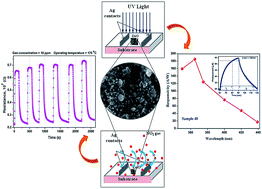
In order to find new approaches for sensor devices; ZnO based gas sensors and UV photodetectors with higher sensitivity and responsivity were fabricated. ZnO thin films were synthesized by using inexpensive successive ionic layers by an adsorption and reaction method (SILAR) on the amorphous glass substrate. The fabricated metal–semiconductor–metal (MSM) UV photoconductive detector shows excellent photoresponse with fast response and recovery times (18 s and 24 s) under UV illumination (wavelength −365 nm and power density −1.8 μW cm−2) at 5 V bias voltage. The detector shows an ohmic nature between metal semiconductor contacts with spectral responsivity 185 A W−1. Gas sensing performance for detecting NO2 gas was studied at a relatively low operating temperature of 175 °C and 20.52 response was observed for the optimized film for a 60 ppm gas concentration. The sensor has good repeatability along with a quick response time, whereas it has a relatively high recovery time. The sensor is highly selective towards NO2 gas as compared to other gases, and has a lower detection limit of 10 ppm at an operating temperature of 175 °C. The present study opens up possibilities for the extensive study of ZnO thin film based sensor devices using a simple chemical deposition method (SILAR).


1 Introduction

Semiconductor devices combining multiple physical and optical phenomena to achieve new functionality are receiving much attention, and are often referred to as multifunctional or smart devices. In addition, many 2D layered nanomaterials such as MoS2, SnS2 etc. have attracted great attention as sensor materials because of their novel and superior optical, electrical, and thermal properties.1 Semiconductor nanostructured materials have enormous potential to exhibit multifunctionality in a single nanostructure. Pawar et al. reported the multifunctional use of V2O5 nanosheets deposited using hydrothermal method, as an ultraviolet photodetector, humidity sensor and flat panel array.2 Nanostructured ZnO thin films have been widely used for many applications because of its eye catching structural and optoelectronic properties. ZnO has wide direct band gap of 3.37 eV and also exhibit large exciton binding energy 60 meV.3 The ZnO thin films have broadly used in various applications such as chemical gas sensor,4 solar cell,5 and UV photodetectors.6 Chemically synthesized UV photodetectors and chemical gas sensors are of great interest because of the low cost of fabrication, low temperature processing and large device area. Recently, an emerging self powered UV photodetectors based on semiconductor oxides exhibits a practical UV detecting application such as environmental monitoring, high temperature flame detection and also in secures space in space communication.7 Several wide gap semiconductor materials such as GaN,8 TiO2 and ZnO9,10 have been studied for UV detectors. Due to the attractive inherent electrical and optical properties of ZnO such as, high electron mobility and high thermal conductivity it is promising candidate for multifunctional application. It emerged as an alternative application for GaN based detectors because of its high exciton binding energy.

There are variety of gas sensors available for the detection of various gases, Late et al. reported the sensing of NH3 gas using single layered MoSe2.11 Among all the gases, recently the detection of NO2 gas has become the research focus due to the environmental problems and it causes hazardous effects on the human health such as breathing, itching and asthma etc12. Usually the gas sensors operated at higher temperature is used for the detection of NO2 gas.13 Therefore, there is requirement of highly sensitive yet low cost gas sensor for monitoring NO2 gas operating at relatively lower operating temperatures. A large variety of NO2 gas sensors have been obtained using various metal oxide semiconductor materials such as WO3,14 ZnO,15 SnO2[thin space (1/6-em)]16 and MoS2.17 Among these material ZnO is one of the candidates for detection of NO2 gas, because of its chemical and thermal stability in the environment of mixtures of various toxic gases.18 Several advanced methods are available for the synthesis of thin films used for the gas sensor application such as electron beam lithography and reactive vapor deposition.19,20 All these techniques demands highly sophisticated instruments with various reaction conditions such as high operating temperature and pressure, hazardous chemicals etc. As compared other techniques, solution based chemical technique such as sol–gel dip coating and chemical bath deposition (CBD) attracted considerable attention, because these techniques are inexpensive and require relatively low deposition temperature. Among these techniques, sol–gel dip coating method requires long reaction time for the formation of gel for synthesis of film. In chemical bath deposition (CBD) technique there is formation of the film, due to controlled chemical reaction in solution bath. Due to the formation of precipitation in reaction bath, there is wastage of solution. To avoid these drawbacks new method is introduced known as modified chemical bath deposition i.e. SILAR method. SILAR technique adopts layer by layer growth mechanism by using separate cationic and anionic precursor for deposition of films at relatively low temperature.21

In this work influence of deposition conditions on the physicochemical, gas sensing and UV detecting properties of ZnO thin film are studied. The performance and sensitivity of ZnO thin film based UV photodetector and NO2 gas sensor is studied at different bias voltages and operating temperatures in the mist of various gases and concentrations. The multifunctional ZnO thin film based sensing devices are prepared by SILAR method on amorphous glass substrate. The effect of deposition cycles on the performance of ZnO MSM UV photoconductive detector and gas sensor is discussed in the present work. This study shows a simple and cost effective alternative to fabricate ZnO thin film based sensor devices.

2 Experimental section

2.1 Materials

Aqueous solution of zinc chloride (ZnCl2) was used as the cationic precursor for the synthesis of ZnO thin films, and aqueous ammonia was used to adjust the pH to 11. Double distilled water (DDW) with two drops of hydrogen peroxide (H2O2) was used as anionic precursor.

2.2 Preparation of films

The ammonium zincate bath22 used as cationic precursor was prepared by adding dropwise 3.8 ml of aqueous ammonia into the 0.1 M ZnCl2 solution with continuous stirring until pH of the solution became 11. The anionic bath was prepared by adding two drops of H2O2 in DDW and kept at 70 °C constant temperature. The process of SILAR involves alternate immersion of substrate in cationic and anionic precursor, followed by rinsing of substrate in DDW after each immersion kept at room temperature.23 During the deposition of ZnO thin films by SILAR method, following steps are involved: (1) immersing the glass substrate in a cationic precursor solution for 30 s to create a thin liquid film which contains zinc complex ion on the substrate. (2) Immediately rinsing this substrate in DDW bath at room temperature, so as to remove loosely bound zinc complex ions from the substrate for 15 s. (3) Then immersing the substrate in an anionic precursor for 30 s, during this process the OH ion from anionic precursor reaction with zinc complex ion to form Zn(OH)2 on the substrate. (4) Finally the substrate was again rinsed in DDW which was kept at room temperature for 15 s, to remove unreacted OH and loosely bonded Zn(OH)2 particles from the substrate. After this film is allowed to dry for 30 second and then next cycles is continued. In this way one SILAR cycle is completed which is then followed by the desired number of cycles. In these experiments number of cycles are varied as 30, 40, 50 and 60 and corresponding films are named as sample 30, sample 40, sample 50 and sample 60, respectively.

2.3 Reaction mechanism

The reaction mechanism involved in ZnO thin film formation can be explained as formation of Zn(OH)2 when aqueous ammonia is added dropwise into the 0.1 M ZnCl2 solution as shown in reaction (1)
 
ZnCl2 + 2NH4OH → Zn(OH)2 + 2NH4+ + 2Cl (1)

When excess aqueous ammonia was added into the solution, then there was formation of zinc complex ion in the solution, when glass substrate was immersed in this solution, zinc complex ions were adsorbed onto the substrate due to the cohesive forces, van-der Waals forces or chemical attractive forces between ions and surface of substrate.24

 
Zn(OH)2 + 4NH4+ → [Zn(NH3)4]2+ + 2H2O + 2H+ (2)

In the anionic precursor when two drops of H2O2 were added in to the DDW then it decomposes in the water and oxygen gas as,

 
2H2O2 → 2H2O + O2 (3)

When the substrate immersed in the anionic precursor then zinc complex ion reacts with water which is kept at 70 °C, to form Zn(OH)2 on the surface substrate.

 
[Zn(NH3)4]2+ + 2H2O + O2 → Zn(OH)2 + 3NH4+ + 2H2O (4)

To obtain pure ZnO, these substrates were annealed at 500 °C in ambient temperature for 4 h resulting into highly crystalline ZnO thin films.

 
Zn(OH)2 → ZnO + H2O (5)

2.4 Materials characterization

The thickness of the all films was measured using XP stylus surface profiler instrument. The crystal structure of deposit films was identified by using X-ray diffraction (XRD) using Bruker D2 phaser with CuKα radiation. The surface morphology of the films was investigated by using scanning electron microscopy (SEM; model: JSM-6701F, Japan) and surface topography of the films was identified using atomic force microscopy (AFM). In order to identify fundamental absorption edge, the room temperature optical absorption measurements were carried out by using Shimadzu UV-Vis-1800 spectrophotometer.

2.5 Device testing

The MSM photoconductive detector was fabricated by using a simple SILAR method with an effective area of (1 × 1 sq. cm). Two silver (Ag) electrodes were printed on the top surface of ZnO thin films which act as metal contacts. AMEL instruments model 2059 electrometer was used to measure current–voltage (IV) characteristics of the fabricated ZnO UV photodetector, with the help of Omnilux UV source of 365 nm wavelength and intensity 1.8 μW cm−2. The intensity of UV source was measured with the help of a Lutron UV light meter having range 290–390 nm. The spectral responsivity measurements were carried out at different wavelengths using light filters. All of the measurements were carried out at room temperature in ambient condition.

To measure the gas sensing properties, thin films were placed in airtight chamber equipped with heater and microcontroller. Thin films sensors were heated at desired temperature for about 1 h and resistance of the sensor was allowed to stabilize which is used as a reference resistance. Later NO2 were introduced into the chamber using air as the carrier gas, and change in the resistance is measured. Gas sensing properties of the films were measured at different operating temperature and at different gas concentrations. Fresh air is passed through the test chamber after each measurement in order to remove trace gases of previous measurement. Change in resistance of the film was measured by using Keithley 6514 electrometer as a function of time. The response of ZnO thin film sensors was defined as S = Rg/Ra; Rg and Ra are the resistance of the sensors in presence of target gas and air, respectively.

3 Results and discussion

3.1 Structural analysis

Fig. 1 shows the XRD patterns of ZnO thin films deposited at various deposition cycles. Peaks well matches with JCPDS card no. 01-071-6424 indicating hexagonal wurtzite crystal structure of the films. It is observed from Fig. 1 that ZnO thin films exhibit most intense peak corresponding to (002) plane at 34.49° and two minor peaks at 31.77° and 36.32° corresponding to (100) and (101) planes. ZnO thin films have preferred orientation along (002) plane indicating perpendicular alignment of the c-axis.
image file: c6ra01750a-f1.tif
Fig. 1 XRD patterns of ZnO thin films deposited at different deposition cycles.

All the films posses hexagonal wurtzite crystal structure whereas intensity and full width half maximum (FWHM) of the peaks changes with film thickness i.e. with change in number of deposition cycles. The value of thickness of all the films is summarized in Table 1 in ESI. Intensity of the peaks increases with increase in deposition cycles till 40 cycles and further decrease for 50 and 60 cycles. Decrease in the peak intensity for 60 cycles is due to the decrease in the films thickness due to peeling off the films from the substrates. The growth of the films is along c-axis i.e. along (002) which is favorable direction and it is also observed from SEM images.

3.2 Morphological analysis

Fig. 2 shows SEM images of prepared ZnO thin films at different deposition cycles. The morphological transformation of ZnO thin films is observed by varying the number of deposition cycles. Change in morphology is typical behavior of progressive nucleation and growth of films by varying deposition cycles. Morphological structure of ZnO films is controlled by the combination of various deposition parameters during SILAR process. At 30 deposition cycles, appearance of some spindle like shape with non uniform distribution is observed (Fig. 2(a)-sample 30). The film starts to grow and a small number of randomly distributed grains are observed. At 40 cycles the density of the particles increase due to agglomeration of smaller crystallites resulted due to increase in deposition cycles. Formation of continuous and finely agglomerated closely spaced particles on the film is observed in Fig. 2(b) (sample 40). Further sample 40 has dual scale morphological structure which is well observed in magnified SEM images (Fig. 2(e)). Since dual scale structure has more surface area than that of the spherical grains; effective surface of sample 40 is higher (Table 1 in ESI) than that of other films which results in superior UV photocurrent and gas response for sample 40. Further higher thickness of the sample 40 is another reason supporting higher gas response and photocurrent than the other films. This ultimately yields a way to increase number of surface sites available for the adsorption of the analyte gases and thereby gas response of the films. When the number of cycles is increased up to 50 cycles, assembly of irregular petal like structure along with some spherical grains is observed (Fig. 2(c)-sample 50). Petals have is non uniform dimensions and are well distributed over the surface of the substrate; it's ranging from 500 nm to 1 μm. By increasing the number of cycles to 60, the morphology of the sample 50 is transferred from the petal like structure to spheres with average diameter of 400 nm to 1 μm (Fig. 2(d)-sample 60). This microstructure found to be uniform with spheres interconnected with each other.
image file: c6ra01750a-f2.tif
Fig. 2 (a–d) SEM images of ZnO thin films deposited at different deposition cycles. (e) Magnified SEM image of sample 40.

The surface topography of ZnO thin films is observed by recording three dimensional AFM micrographs over (5 μm × 5 μm) scanning area as shown in Fig. 3. It is seen that grains are uniformly distributed over the substrates and some individual grains extending upwards indicating growth of the films perpendicular to the substrates for all the films. The root mean square (rms) surface roughness and grain diameter of ZnO thin films is shown in Table 1 in ESI. It is observed that roughness of the films increase up to sample 40 and after that it decreases and the value of the grain diameter also highest for sample 40. Maximum surface roughness provides more effective surface area and thus improves gas and UV response. Dual scale morphology for sample 40 is also observed in Fig. 3 (sample 40). Micrographs indicate that the orientation of grains is perpendicular to the surface of the substrates, i.e. oriented along the c-axis which is also confirmed from the XRD analysis.


image file: c6ra01750a-f3.tif
Fig. 3 AFM images of ZnO thin films deposited at different deposition cycles.

3.3 Optical analysis

The energy band gaps of films were determined by using the optical absorption spectra. The optical band gaps were estimated by using the following equation,
 
image file: c6ra01750a-t1.tif(6)
where A is constant, Eg is the optical band gap, and n = 1/2 for direct allowed transition and n = 2 for allowed indirect transition.25 The optical band gap (Eg), was estimated from the extrapolation of the linear portion on the energy axis in a plot of (αhυ2) against (). The variation of absorbance (αt) of the ZnO thin films sample 30, sample 40, sample 50 and sample 60 with wavelength λ is shown in Fig. 4. Less absorption in the visible region of the spectrum and high absorption in the UV region of the spectrum are observed for the films. The absorption edge of the films is around 360 nm, indicating that the ZnO thin film have the characteristic of preferred absorption of UV light. Absorbance of the films decreases with increase in deposition cycles because of increase in the thickness of the films resulted due to deposition of large amount of material on the substrates.26 Due to high temperature synthesis defects are formed in thin films usually oxygen deficiencies which form unsaturated bonds in the films. These unsaturated bonds produce localized states in the films. With increase in the thickness of film, density of localized states in the optical band gap increases. Thus the optical absorption edge decreases with reverse effect. The slight variation in band gap values is observed with variation in deposition cycles this may be due to the slight variation in the stoichiometric changes in the films. The straight portion in higher energy region confirms that the direct allowed transition in ZnO thin film.

image file: c6ra01750a-f4.tif
Fig. 4 Optical absorption spectra of ZnO thin films deposited at different deposition cycles. Inset; Tauc plot determining band gap energy of the films.

3.4 UV sensing properties

3.4.1 IV characteristics. Fig. 5 shows typical current–voltage (IV) characteristic of fabricated ZnO based MSM photodetectors with Ag as contact electrodes measured under 1.8 μW cm−2 UV light illumination (λ = 365 nm), with 5 V bias voltage. The inset of Fig. 5 shows the device structure of MSM UV photodetector. The net photocurrent is obtained by subtracting dark current from obtained photocurrent (Iph = IlightIdark), as dark current is relatively low as compared to the photocurrent. Ag contact electrode plays important role in rapidly transforming photoelectrons in ZnO thin film to the electrode. The linearity of the IV curves indicates ohmic nature of the contact between Ag electrode and working electrode. As shown in figure there is a significant increase in the photocurrent up to sample 40 and then it decreases. The highest photocurrent observed is 55.74 μA for sample 40. Maximum photocurrent observed for sample 40 is attributed to the higher crystallinity, surface roughness and thickness of the sample 40 as discussed earlier. Photocurrent is highest for sample 40, which related to a lower density of grain boundaries and accordingly lower density of the defects. The highest value of grain diameter is for sample 40 (Table 2 in ESI); due to this sample 40 seems to have lowest contact resistance, and therefore it is less electrically compensated. During the UV sensing measurement oxygen chemisorption plays an important role in regulating the photosensitivity of ZnO thin film. In dark condition oxygen molecules from ambient atmosphere adsorbs on the surface of the ZnO thin film as negatively charged ions by capturing free electrons from the n-type ZnO. Therefore creating a low conductivity depletion region near the surface of thin film. Under UV illumination, the electron hole pairs are created by absorption of UV radiations. These electron–hole pairs then migrates along the surface of the film to discharge the adsorbed oxygen ions by surface electron–hole recombination. At the same time, the remaining are the majority carriers electrons in the device, which contributes to the photocurrent.27
image file: c6ra01750a-f5.tif
Fig. 5 IV characteristics of ZnO thin film based UV photodetectors measured in dark and under 365 nm illumination. Inset; schematic of fabricated MSM UV photodetector.
3.4.2 Photoswitching characteristics. The response behavior of the device is characterized by measuring the current under the fixed 5 V bias voltage as function of time. Device is periodically exposed to the UV light at the interval of 30 s and consecutive transient curves are recorded. The time resolved photoresponse current curve of the device in “on” and “off” state (at 5 V bias and 1.8 μW cm−2 UV light illumination) is as shown in Fig. 6(a). The ZnO based MSM UV photodetector shows reproducible characteristics having maximum photoresponse of 55.19 μA for sample 40. It is seen from Fig. 6(a) that the photocurrent doesn't reach its initial value this is due to the persistent photoconductivity in the device.28 In this phenomenon photocurrent persists for a long time in the device after the light is off. The photocurrent rise time and fall time are the key parameters for determining the response kinetics of the detector to a fast varying optical signal. The rise time is the time required to raise the photocurrent from 10% to 90% of its maximum value and for decay time to drop the photocurrent from 90% to 10% of its maximum value.29 Fig. 6(b) shows single time dependent on/off cycle of the detector, also indicating the rise time and fall time with values 18 s and 24 s, respectively. Initially under the UV illumination photocurrent increases sharply and then gradually reaches the maximum. Further when light is turned off, at first current decreases fast and later it achieves value slightly higher than its initial value. Slightly higher values of current after each cycle is due to the persistent photoconductivity (PPC) effect. In PPC effect the photocurrent in the detector continues to flow even after the UV source is turned off. Due to PPC effect photocurrent failed to achieve the original value in dark. As discussed earlier during the photodetection process surface electron–hole recombination takes place. At this time fraction of holes accumulate near the surface of the film, which are then unable to take part in recombination process. Due to the insufficient number of holes, electrons in conduction band or entrapped at the trap centers fails take part in successive recombination. As a result number of electrons are available in conduction band and at the trap centers even after UV source is off.30 It is clear that electron density in the conduction band increases in every cycle during on–off condition. Increase in electron density in the conduction band is correlated with the increase in photocurrent after each cycle.
image file: c6ra01750a-f6.tif
Fig. 6 (a) The current curve of ZnO UV photodetector at a 5 V bias voltage under illumination of an incident light intensity of 1.8 μW cm−2, showing on/off switching behavior. (b) Photoresponse for pulse signal used for determination of rise and fall time of the sample 40.
3.4.3 Responsivity of the MSM UV photoconductive detector as a function of wavelength. The ZnO thin film has high band gap energy (3.37 eV),31 so high response in the UV region of the spectrum is expected. However, at particular wavelength highest responsivity is obtained and that must be determined for commercial application of the UV photodetector. Therefore, responsivity is an essential parameter while determining the performance of the detector. The responsivity (R) of the detector is calculated by using the formula,
 
image file: c6ra01750a-t2.tif(7)
where, IP is the photocurrent of the detector and Popt is the incident power.32 Fig. 7 shows spectral responsivity of ZnO MSM UV photoconductive detector as a function of wavelength. The peak responsivity is observed to be 185 A W−1 at 365 nm under 5 V bias for sample 40. The spectral responsivity of the detector is measured within the wavelength range 340–440 nm. From these measurements it is observed that detector shows an evident response in the UV region of the spectrum and less response in the visible region. The responsivity of the detector increases until it reaches the maximum at 365 nm and then decreases on the higher wavelength side. It is clearly observed that responsivity of the detector strongly depends on wavelength of UV illumination sources. The obtained responsivity is much higher than those reported earlier for ZnO based UV photodetectors obtained by using various deposition techniques. The relative value of responsivity of ZnO based UV photodetector fabricated using different techniques from various reports are summarized in Table 2 in ESI for comparison.33–37

image file: c6ra01750a-f7.tif
Fig. 7 Spectral response of ZnO thin film UV photodetector at different wavelengths. Inset; variation of responsivity with number of deposition cycles.
3.4.4 UV photoconductive detector light intensity dependent property. Photocurrent of the fabricated UV photodetector exhibits strong dependence on the intensity of the incident UV light of wavelength 365 nm at 5 V bias. The corresponding dependence of photocurrent on the light intensity can be expressed as a power function of incident light intensity (P),
 
IPCPθ (8)
where IPC is photocurrent, P is intensity of illumination and θ determines the response of photocurrent to light intensity.38 Fig. 8(a) and (b) shows graph of power density vs. photocurrent and its logarithmic plot. As illumination power increases, photocurrent of the photodetector increases. In other words number of photons were irradiated on the ZnO thin film, more charge carriers were generated, and indicating that good photoresponse capability of ZnO based MSM UV photodetector. The light intensity dependent property of the photodetector exhibits the promising potential as a photo switch and a highly sensitive photodetector. Fig. 8(b) shows the power law dependency of photocurrent. Linear fitting of the points in Fig. 8(b) is carried out and value of exponent is obtained and corresponding power law relations (or equations) are summarized in Table 3 in ESI. The variation in the non-integer exponent ‘θ’ of the devices at various deposition cycles is shown in Table 3 in ESI. When θ tends to 1, all recombination centers are supposed to be empty, which indicates the monomolecular recombination in the bulk. There is bimolecular recombination at the surface if θ is 0.5. When the value of θ is greater than one (θ > 1), it suggest that there is complex process of electron–hole pair generation, trapping of the holes and recombination during the photoresponse process for the UV photodetector. The relatively high value of exponent ‘θ’ for sample 40, may be related to surface chemisorbed oxygen molecules which leads to the excellent UV response. These three parameters had major contributing parameters of the photocurrent generation in ZnO thin films.39

image file: c6ra01750a-f8.tif
Fig. 8 UV light intensity dependent property of ZnO thin film based UV photodetector. (a) Dependence of the photocurrent on optical power density of UV light of wavelength 365 nm at 5 V bias (b) fitting of the power law to the graph of photocurrent versus power density at 5 V bias voltage.

3.5 NO2 sensing studies

3.5.1 NO2 sensing mechanism. The gas sensing mechanism of ZnO thin film involves the change in the surface resistance of the film due to the chemisorption of oxygen onto the surface. During the gas sensing measurement, when the ZnO thin film based sensor exposed to air at high temperature, oxygen molecules are absorbed on the sensor surface as negatively charged ions by capturing free electrons from the n-type of ZnO. This results in increase in the resistance of n type material and vice versa for p type material.40

When a ZnO thin film sensor in equilibrium with atmosphere is exposed to NO2 gas, NO2 is adsorbed on it and subsequently it captures one more electron from the conduction band of the sensor. This leads to the chemisorption of NO2 as NO2, in so doing concentration of the majority charge carriers is decreased and this results in increase in resistance of the sensor. The desorption of NO2 gas is also taking place. Further adsorbed monomolecule of oxygen is dissociated when NO2 approaches to the adsorbed site and monomolecule of oxygen is dissociated and chemisorbed as atomic oxygen ionic species. Due to this there is a decrease in concentration of conduction electrons in the surface layer of the semiconductor sensor, which leads to the increase in resistance of the sensor material.41

 
NO2(gas) + e → NO2(ads) (9)
 
NO2(gas) + O2 + 2e → NO2(ads) + 2O(ads) (10)

3.5.2 Selectivity and determination of operating temperature of ZnO thin film based gas sensor. Selectivity of the sensor is the ability to respond to a particular gas in the presence of other gases. Gas response depends on many factors such as adsorbed oxygen species, adsorption and desorption rate of analyte gas and operating temperature. Among which operating temperature plays an important role during gas sensing and selective detection of gases. Fig. 9 shows the bar diagram of gas response of ZnO thin films to different gases at different operating temperatures. To obtain optimum operating temperature the ZnO thin films were exposed to various gases at a concentration of 100 ppm, within the 100–225 °C temperature range. From the figure it is clear that ZnO thin film has maximum response towards NO2 gas at operating temperature 175 °C as compared to other gases, the maximum response observed was 31.10 towards 100 ppm NO2 concentration. The figure indicates that films are highly selective to NO2 at 175 °C operating temperature and gas response decreases on either side of this temperature. Among all the four films, sample 40 shows better gas response as compared to other films. It is believed that 175 °C is optimum operating temperature for the ZnO thin film based NO2 sensor. Hence, further gas sensing measurements are carried out at 175 °C operating temperature. The obtained operating temperature is low as compared to the other ZnO thin film based sensor.42,43 The n-type ZnO thin films are electron rich, hence they provides higher binding affinity for electron withdrawing molecules, such an approach allowed the selective detection of NO2 gas. This further enhanced by higher electron affinity of nitrogen (2.28 eV) as compared to the other gases. The chemisorbed molecules and/or gas reaction species take some time to leave the sensor surface after completion of the reaction and/or after removing NO2 gas resulting in decrease in desorption rate which increases the recovery time.2 During the sensing process, the adsorption of electron-withdrawing NO2 molecules compensates for the hole carriers in the n-type ZnO, causing the electrical resistance of the ZnO thin film to increase with concentration of NO2.
image file: c6ra01750a-f9.tif
Fig. 9 Selectivity study of ZnO thin films deposited at various deposition cycles towards various gases at different operating temperature for 100 ppm gas concentration.

Selectivity coefficient is direct measure of selective detection of target gas in presence of other gases. It is calculated using formula

 
image file: c6ra01750a-t3.tif(11)
where k is selectivity coefficient St is the gas response to target gas (NO2) and Si is gas response to interfering gas. Variation in selectivity coefficient at 175 °C is mentioned in Table 4 in ESI. Higher response observed to NO2 in presence of various gases is due to high reactivity and higher electron affinity (2.28 eV) of NO2, in comparison with preadsorbed oxygen (0.43 eV) and other test gases. The oxygen deficient sensor surface increases the number of sites for the adsorption of the NO2 thereby making films selective towards NO2 than other gases. Selective detection of NO2 in presence of various gases is discussed elsewhere.44

3.5.3 Gas sensing studies. Fig. 10 shows dynamic response curve of ZnO thin film at different operating temperature at 60 ppm NO2 gas concentration. As operating temperature increases gas response also increases up to temperature 175 °C and then gas response decreases with further increase in operating temperature. At 175 °C temperature more number of adsorbed oxygen species are available to react with the NO2 gas, therefore gas response increases at particular operating temperature. Sample 40 shows 20.52 gas response at 175 °C operating temperature higher than the other operating temperature. It is seen that sensor resistance does not recover to its initial value within the given interval of time. At lower operating temperature response and recovery reactions are slow and it increases with increase in operating temperature. Response and recovery time of sample 40 at different operating temperature was calculated and shown in Table 5 in ESI. It is observed that response time decreases with an increase in operating temperature and remains constant for higher operating temperature. Recovery time also decreases with an increase in operating temperature. Recovery time is higher than the response time. Because sample 40 has porous morphology, due to this more time is required for gas molecules to desorb form the sensor surface. The major key factors limiting response speed is the transducer function of the sensor which decreases with increase in grain size. This can be overcome by increasing transducer function by depositing thin layer of nobel metal like Pd or Pt on the sensor surface. Thin layer of nobel metal acts as catalysts and thereby improves adsorption reaction and thus reaction rate of the films. Further for sample 40 change in resistance upon introduction of NO2 gas is higher, thus it takes longer time to occur that change in resistance.
image file: c6ra01750a-f10.tif
Fig. 10 Dynamic response curve of ZnO thin film (sample 40) at different operating temperature for 60 ppm NO2 gas concentration.

Variation in resistance of the sample 40 towards various NO2 concentrations ranging from 20 to 100 ppm at 175 °C operating temperature is shown in Fig. 11(a). As expected resistance of the sensor increases with increase in NO2 gas concentration. Variation in resistance is less for lower NO2 concentration and the value of resistance increases rapidly as concentration increased from 20 ppm to 60 ppm and it increases gradually for 80 ppm and 100 ppm. The resistance of the film increases upon exposure to NO2 gas, and recovered to the value slightly higher that initial value after removing the NO2 gas. To attain the saturation, we kept NO2 gas for around 2 minutes in the chamber and then outflow valve is opened. A slightly higher value than the initial value is due to the incomplete removal of the adsorbed gas even after removal of NO2. Small amount of traces of NO2 remains adsorbed on the sensor surface thus a slight increase in resistance of the sensor is observed with consecutive cycles. The sensor response is stable and reproducible at a repeated number of cycles of optimized film. The maximum gas resistance is observed at 100 ppm gas concentration; because of high concentration there is sufficient number NO2 gas molecules available to react with surface oxygen adsorption sites. The response and recovery time of the film also increases simultaneously as shown in Fig. 11(b). The value of response time increases as NO2 gas concentration increase and it is nearly same for 80 ppm and 100 ppm gas concentration. The recovery is also increased linearly with increase in NO2 gas concentration. The recovery time is higher than the response time and reason for higher deposition time is as mentioned in the above paragraph. To check the reproducibility of the sample 40, is exposed to 10 ppm NO2 gas concentration at operating temperature 175 °C in six successive cycles of measurement as shown in Fig. 11(c). It can be seen that, during long time continuous operation, response of the sensor gives stable resistance value for over two minutes and then resistance starts to recover when outflow valve is opened. The reversible response curve indicates that NO2 gas shows relatively stable and repeatable response at lower gas concentration.


image file: c6ra01750a-f11.tif
Fig. 11 (a) Transient gas response of sample 40 film at 175 °C operating temperature towards various NO2 gas concentrations. (b) Variation of response and recovery time with various NO2 gas concentrations (c) reproducible transient gas response of film towards 10 ppm NO2 concentration at 175 °C operating temperature.

4 Conclusions

In this study, a successful attempt has been made to fabricate multifunctional ZnO thin film based MSM UV photoconductive detector and NO2 gas sensor, using SILAR method. Effect of number of deposition cycles on the morphology and photodetective properties of the device has investigated. The sample 40 shows highest photoresponsivity as well as highest gas response towards NO2 gas at 175 °C operating temperature. The ZnO thin film based photodetector is visible blind and shows effective response in the mid UV region. The fabricated device exhibits good photoconductivity, responsivity and fast photoswitching characteristic having highest responsivity of 185 A W−1. Gas response of ZnO thin film at different operating temperature along with selectivity is investigated. The sample 40 ZnO thin film shows high gas response, reproducibility and selectivity towards NO2 gas at relatively low operating temperature of 175 °C with 10 ppm lower detection limit. The highest gas response observed towards 100 ppm NO2 is 31.10 at moderately low operating temperature of 175 °C. Lower detection limit achieved is 10 ppm with gas response of 2.83 in 12 s for the sample 40 at 175 °C towards 10 ppm NO2 concentration. The sensor shows fast response time but recovery time is relatively higher as compared with response time. The result suggests the dual potential use of ZnO thin film as a gas sensor application for NO2 gas and UV photodetector. The present study provides a novel platform for designing MSM UV photodetector for enhanced UV detection. The best result achieved with simple deposition technique SILAR with simple sensor preparation technology. The results seem to lead to the new opportunities for the low cost fabrication of ZnO based multifunctional sensor devices.

Acknowledgements

S. I. Inamdar and V. V. Ganbavle are very thankful to UGC New Delhi, for providing financial support through Maulana Azad, SRF, and UGC-BSR, SRF, respectively.

References

  1. P. K. Kannan, D. J. Late, H. Morgan and C. S. Rout, Nanoscale, 2015, 7, 13293 RSC.
  2. M. S. Pawar, P. K. Bankar, M. A. More and D. J. Late, RSC Adv., 2015, 5, 88796 RSC.
  3. Y. Zeng, X. Pan, W. Dai, Y. Chen and Z. Ye, RSC Adv., 2015, 5, 66738 RSC.
  4. V. V. Ganbavle, S. I. Inamdar, G. L. Agawane, J. H. Kim and K. Y. Rajpure, Chem. Eng. J., 2016, 286, 36 CrossRef CAS.
  5. Q. Zhang, C. S. Dandeneau, X. Zhou and G. Cao, Adv. Mater., 2009, 21, 4087 CrossRef CAS.
  6. X. G. Zheng, Q. S. Li, J. P. Zhao, D. Chen, B. Zhao, Y. J. Yang and L. C. Zhang, Appl. Surf. Sci., 2006, 253, 2264 CrossRef CAS.
  7. Y. Cao, S. Deng, Q. Hu, Q. Zhong, Q.-P. Luo, L. Yuan and J. Zhou, RSC Adv., 2015, 5, 85969 RSC.
  8. H. Morkoc, A. D. Carlo and R. Cingolani, Solid-State Electron., 2002, 46, 157 CrossRef CAS.
  9. H. Huang, Y. Xie, Z. Zhang, F. Zhang, Q. Xu and Z. Wu, Appl. Surf. Sci., 2014, 293, 248 CrossRef CAS.
  10. X. Zhang, X. Han, J. Su, Q. Zhang and Y. Gao, Appl. Phys. A, 2012, 107, 255 CrossRef CAS.
  11. D. J. Late, T. Doneux and M. Bougouma, Appl. Phys. Lett., 2014, 105, 233103,  DOI:10.1063/1.4903358.
  12. V. V. Ganbavle, M. A. Patil, H. P. Deshmukh and K. Y. Rajpure, J. Anal. Appl. Pyrolysis, 2014, 107, 233 CrossRef CAS.
  13. M. Epifani, R. Díaz, J. Arbiol, E. Comini, N. Sergent, T. Pagnier, P. Siciliano, G. Faglia and J. R. Morante, Adv. Funct. Mater., 2006, 16, 1488 CrossRef CAS.
  14. L. G. Teoh, Y. M. Hon, J. Shieh, W. H. Lai and M. H. Hon, Sens. Actuators, B, 2003, 96, 219 CrossRef CAS.
  15. X. Wang, F. Sun, Y. Duan, Z. g. Yin, W. Luo, Y. Huang and J. Chen, J. Mater. Chem. C, 2015, 3, 11397 RSC.
  16. A. Sharma, M. Tomar and V. Gupta, Sens. Actuators, B, 2013, 181, 735–742 CrossRef CAS.
  17. D. J. Late, Y. K. Huang, B. Liu, J. Acharya, S. N. Shirodkar, J. Luo, A. Yan, D. Charles, U. V. Waghmare, V. P. Dravid and C. N. R. Rao, ACS Nano, 2013, 7, 4879 CrossRef CAS PubMed.
  18. G. H. Mhlongo, D. E. Motaung, I. Kortidis, N. R. Mathe, O. M. Ntwaeaborwa, H. C. Swart, B. W. M. wakikunga, S. S. Ray and G. Kiriakidis, Mater. Chem. Phys., 2015, 162, 628 CrossRef CAS.
  19. D. Padilla-Rueda, J. M. Vadillo and J. J. Laserna, Appl. Surf. Sci., 2012, 259, 806 CrossRef CAS.
  20. L. Liao, H. B. Lu, J. C. Li, H. He, D. F. Wang, D. J. Fu and C. Liu, J. Phys. Chem. C, 2007, 111, 1900 CAS.
  21. I. Barcelo, T. Lana-Villarreal and R. Gomez, J. Photochem. Photobiol., A, 2011, 220, 47 CrossRef CAS.
  22. P. Mitra and J. Khan, Mater. Chem. Phys., 2006, 98, 279 CrossRef CAS.
  23. P. S. Kumar, A. D. Raj, D. Mangalaraj and D. Nataraj, Thin Solid Films, 2010, 518, e183 CrossRef.
  24. H. M. Pathan and C. D. Lokhande, Bull. Mater. Sci., 2004, 27, 85 CrossRef CAS.
  25. M. Ali Yıldırım and A. Ates, Opt. Commun., 2010, 283, 1370 CrossRef.
  26. E. S. M. Goh, T. P. Chen, C. Q. Sun and Y. C. Liu, J. Appl. Phys., 2010, 107, 024305 CrossRef.
  27. Y. Li, F. D. Valle, M. Simonnet, I. Yamada and J. J. Delaunay, Nanotechnology, 2009, 20, 045501 CrossRef PubMed.
  28. Y. K. Su, S. M. Peng, L. W. Ji, C. Z. Wu, W. B. Cheng and C. H. Liu, Langmuir, 2010, 26, 603 CrossRef CAS PubMed.
  29. J. Liu, N. Motta1 and S. Lee, Beilstein J. Nanotechnol., 2012, 3, 353 CrossRef PubMed.
  30. S. Kumar, G. H. Kim, K. Sreenivas and R. P. Tandon, J. Phys.: Condens. Matter, 2007, 19, 472202 CrossRef.
  31. X. D. Gao, X. M. Li, W. D. Yu, L. Li, F. Peng and C. Y. Zhang, J. Cryst. Growth, 2006, 291, 175 CrossRef CAS.
  32. N. K. Hassan, M. R. Hashim, K. Al-Heuseen and Nageh K. Allam, Chem. Phys. Lett., 2014, 604, 22 CrossRef CAS.
  33. L. Guo, H. Zhang, D. Zhao, B. Li, Z. Zhang, M. Jiang and D. Shen, Sens. Actuators, B, 2012, 166–167, 12 CrossRef CAS.
  34. N. Liu, G. Fang, W. Zeng, H. Zhou, F. Cheng, Q. Zheng, L. Yuan, X. Zou and X. Zhao, ACS Appl. Mater. Interfaces, 2010, 2, 1973 CAS.
  35. Y. Liang, H. Liang, X. Xiao and S. Hark, J. Mater. Chem., 2012, 22, 1199 RSC.
  36. Y. Jin, J. Wang, B. Sun, J. C. Blakesley and N. C. Greenham, Nano Lett., 2008, 8, 1649 CrossRef CAS PubMed.
  37. G. Li, J. Song, J. Zhang and X. Hou, Solid-State Electron., 2014, 92, 47 CrossRef CAS.
  38. Z. Liu, B. Liang, G. Chen, G. Yu, Z. Xie, L. Gao, D. Chen and G. Shen, J. Mater. Chem. C, 2013, 1, 131 RSC.
  39. R. R. Prabhakar, N. Mathews, K. B. Jinesh, K. R. G. Karthik, S. S. Pramana, B. Varghese, C. H. Sowc and S. Mhaisalkar, J. Mater. Chem., 2012, 22, 9678 RSC.
  40. C. Zou, F. Liang and S. Xue, Appl. Surf. Sci., 2015, 353, 1061 CrossRef CAS.
  41. R. C. Pawar, J. W. Lee, V. B. Patil and C. S. Lee, Sens. Actuators, B, 2013, 187, 323 CrossRef CAS.
  42. S. Ozturk, N. Kilinc, N. Tasaltin and Z. Z. ozturk, Thin Solid Films, 2011, 520, 932 CrossRef CAS.
  43. M. A. Chougule, S. Sen and V. B. Patil, Ceram. Int., 2012, 38, 2685 CrossRef CAS.
  44. V. V. Ganbavle, S. V. Mohite, G. L. Agawane, J. H. Kim and K. Y. Rajpure, J. Colloid Interface Sci., 2015, 451, 245 CrossRef CAS PubMed.

Footnote

Electronic supplementary information (ESI) available. See DOI: 10.1039/c6ra01750a

This journal is © The Royal Society of Chemistry 2016
Click here to see how this site uses Cookies. View our privacy policy here.