Asymmetric immobilization of antibodies on a piezo-resistive micro-cantilever surface

Dilip Kumar Agarwal*ab, Nidhi Maheshwaria, Soumyo Mukherjiabc and V. Ramgopal Rao*ab
aCentre of Excellence in Nanoelectronics, Dept. of Electrical Engineering, IIT Bombay, Mumbai, India. E-mail: rrao@ee.iitb.ac.in; dilip_agarwal@iitb.ac.in
bCentre for Research in Nanotechnology and Science, IIT Bombay, Mumbai, India
cDepartment of Biosciences and Bioengineering, IIT Bombay, Mumbai, India

Received 17th January 2016 , Accepted 2nd February 2016

First published on 3rd February 2016


Abstract

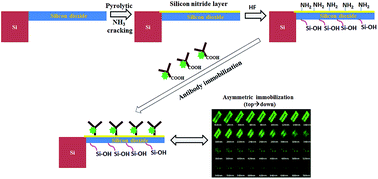
For cantilever-based MEMS sensors, selective chemical modification of the sensing surface is used for the detection of chemical and biological analytes. One of the key challenges in these kind of applications is to obtain an increased level of sensitivity, which largely depends on the surface coverage of the respective probe molecules on one of the cantilever surfaces (asymmetric immobilization). Usually, a blocking layer of another material like gold is deposited on one side of the cantilever surface to obtain layers with different chemical properties. In this paper, we report a novel approach of grafting antibodies on a single side of micro-fabricated piezo-resistive cantilevers. The microcantilevers were fabricated with polysilicon as the piezo-resistive layer, sandwiched between silicon dioxide structural layers. In order to immobilize antibodies on one of the cantilever surfaces (top or bottom), a thin layer of amorphous silicon was deposited on the surface where immobilization needs to be done. This amorphous silicon layer was partially modified into silicon nitride by a Hot-Wire Chemical Vapour Deposition (HWCVD) mediated pyrolytic ammonia-cracking process. The developed selective surface modification protocol for nitride and silicon dioxide surface was studied using X-ray photoelectron spectroscopy (XPS), ellipsometry and contact-angle goniometry. The protocol was first developed on silicon wafer surface, further extending its application onto the piezo-resistive micro-cantilevers. Consequentially, asymmetric immobilization was successfully carried out by selectively grafting antibodies onto the top (modified into nitride) surface of the micro-cantilever by passivating the bottom oxide surface. It was verified using fluorescence microscopy and laser confocal microscopy. Further, we have demonstrated that asymmetrically modified cantilevers show an increased electrical response (20–100%) in comparison to symmetrically modified ones.


1. Introduction

Miniaturized MEMS-based piezo-resistive microcatilevers have been used over the years for biomedical applications due to their fast response, better sensitivity, reliability, large dynamic range and label free detection.1 Due to their high surface to volume ratio, cantilevers show large surface stress generation by surface analyte interaction. Cantilever sensors are mainly operated in static (bending) and dynamic (resonant) mode.2 The piezoresistive effect describes the change in the electrical resistance of a material due to applied mechanical strain, leading to differential surface stress generation and subsequent bending of the sensor.3 Different researchers have used piezo-resistive cantilevers for a variety of biomedical applications. Wee et al.4 used piezo-resistive cantilevers for the detection of prostate specific antigen (PSA) which is a specific marker of prostate cancer. Microcantilevers have been used to detect CRP and myoglobin, important cardiovascular disease markers in the blood serum.5,6 Pei et al.7 reported a method to use piezo-resistive microcantilevers as a glucose biosensor, by detecting biologically relevant glucose concentration upon immobilizing glucose oxidase onto the microcantilever surface. Piezo-resistive silicon nitride cantilevers have also been used for the study of DNA–DNA hybridization and detection of SNP (single nucleotide polymorphism) associated with many genetic diseases.8 Seena et al.9 used piezo-resistive nanocomposite polymer cantilevers for the detection of explosives in vapour phase.

Immobilization (covalent) of biomolecules on the sensor surface is a crucial prerequisite for biosensor applications. Immobilization helps in stability and maintaining proper orientation of bio molecules on the sensor surface which increase their binding efficiency and helps in easy detection.10,11 Receptor molecules attach on only one side of the suspended cantilever sensors in case of asymmetric immobilization in contrast to symmetric immobilization where analytes bind on both surfaces of a cantilever. When analytes bind symmetrically on the cantilever surface, stress is generated on both sides of the surface diminishing the resultant stress resulting in a reduced sensitivity.12 In static mode, asymmetric binding of biomolecules on the cantilever surface plays a key role in enhancing the sensitivity of microcantilever based sensors. In case of asymmetric immobilization, stress will be generated only on one side of the sensor surface leading to a resultant surface stress and subsequent cantilever bending. Fig. 1 shows the schematic of symmetric and asymmetric immobilization.


image file: c6ra01440b-f1.tif
Fig. 1 Schematic showing immobilization and the resultant surface stress generation on cantilever surface, (a) symmetric immobilization (b) asymmetric immobilization of antibodies.

Though, there are a lot of methods published for oriented immobilization of biomolecules on a sensor surface, asymmetric immobilization has still not been studied to a large extent for cantilever based biosensors operating in the surface stress mode. Different groups have used various approaches to modify the sensing surface in order to immobilize biomolecules asymmetrically. In this paper, we are demonstrating the applicability of selectively modifying one surface of the cantilever by using hydrofluoric acid (HF), as mentioned further. Other groups have achieved similar goals by modifying one side of the cantilever with PEG or gold. We show that asymmetric modification by treating the cantilever surface with HF leads to enhanced sensitivity (in comparison to unmodified one), the results of which are further discussed in the paper.

To achieve asymmetric binding of the probe molecules, either the structural layers of the cantilever are made different allowing for selective surface modification (chemically or physically) or a blocking polymeric layer needs to be added on one of the surfaces. A general approach for antibody immobilization on any sensor surface is through a deposition of a thin layer of gold and subsequent functionalization of the gold surface. This is a standard approach which has been reported in many of the published papers.13–17 However, for cantilever sensors, addition of gold increases the stiffness of the cantilever in addition to introducing a bimetallic effect to the structure. As a result, one would not only lose the sensitivity but the sensor also exhibits a high temperature variability.18 Also, these approaches form a layer of randomly oriented antibody molecules on the cantilever surface, thereby generating conformational heterogeneity as well as inactive receptor molecules.19 Since our approach does not require a gold surface, our method bypasses the stiffness problem that the researchers might face as mentioned above; and problems that might occur due to other approaches reported in the literature. Poly ethylene glycol (PEG)-modified silane has been used, as an antifouling agent to block one of the sensor surfaces preventing any kind of molecular adsorption or protein binding.20,21 Researchers have also used nano-dispenser in order to functionalize one side of the cantilever surface by dispensing nano-litre volume drop of the analytes without modifying the other side. Bietsch et al.22 used functionalization method by using inkjet printing to modify one side of cantilever surface by dispensing nano-sized drop of single stranded DNA on thiolated self-assembled monolayers. The major limitation of this approach is to maintain a controlled humid environment so that a sufficient incubation time is allowed for the chemical reaction to occur on the surface.

In this work, we demonstrate a novel method to asymmetrically immobilize functional moieties on the piezo-resistive silicon dioxide–polysilicon–silicon dioxide micro-cantilevers surface. The aim of this work is to demonstrate the surface modification and asymmetric immobilization of antibodies in an elaborate manner. The top silicon dioxide surface of the cantilever was modified using a gaseous reaction at low temperatures in order to form a silicon nitride layer selectively on the exposed side. This was achieved by depositing a thin layer of amorphous silicon on the released cantilever surface followed by a pyrolytic ammonia cracking using Hot-Wire Chemical Vapor Deposition at low temperatures (<100 °C). This method has been successfully demonstrated to create asymmetric surfaces of nitride and oxide on the oxide–polysilicon–oxide cantilevers. The difference in the surfaces was further exploited to develop a selective immobilization protocol for antibodies. The modified surfaces were studied using surface characterization methods like XPS, ellipsometry and contact angle measurement. The efficacy of the developed protocol for asymmetric immobilization on the microcantilever surface was studied using fluorescence and laser confocal microscopy.

2. Materials and experimental methods

Silicon wafers (P-type, 〈100〉, single side polished) were used for carrying out surface modification and immobilization experiments. Silicon dioxide–p-polysilicon–silicon dioxide piezo-resistive cantilevers were fabricated in collaboration with NanoSniff Technologies Pvt. Ltd, IIT Bombay. Human Immunoglobulin antibody (HIgG), Rabbit-anti-HIgG tagged with FITC and Bovine Serum Albumin (BSA) were purchased from Sigma Aldrich. Glutaraldehyde was purchased from SD Fine Chem. India Ltd. Hydrofluoric Acid (49%) was purchased from J.T Baker, USA. Phosphate buffer saline (PBS, 0.008 M sodium phosphate dibasic, 0.002 M sodium phosphate monobasic, 0.137 M sodium chloride, 2.7 M potassium chloride, pH 7.4) and PBS-T (10× PBS containing 0.05% Tween 20) were purchased from Sigma Aldrich. Electrical measurement set-up for cantilever sensitivity experiment was procured from NanoSniff Technologies Pvt. Ltd, IIT Bombay.

2.1. Experimental methods

2.1.1. Cantilever fabrication and design. Silicon dioxide–p-polysilicon–silicon dioxide piezo-resistive cantilevers used for this work were developed in collaboration with Nanosniff Technologies Pvt. Ltd, IIT Bombay. A six inch double sided polished P-type Si wafer of orientation (100) and with resistivity 4–7 ohm cm was first RCA cleaned and subsequently oxidized up to 500 nm using wet thermal oxidation process. RCA (Radio Corporation of America) is a standard wafer cleaning procedure used in microelectronics industry to remove the metal contamination and organic impurities.23 Thereafter, p-polysilicon piezo-resistive layer of thickness 50 nm was deposited by LPCVD (Low Pressure Chemical Vapour Deposition) process24,25 and patterned using a standard micro fabrication process. In order to define the electrical contacts, Cr/Au of thickness 20/200 nm respectively were sputtered and patterned. A silicon dioxide layer of 100 nm thickness was used as a passivation layer for encapsulation. Finally, micro cantilever dies (chips) were released from the back side using TMAH (Tetra Methyl Ammonium Hydroxide) wet etching process. A cantilever ‘die’ means an individual sensor device and in our case each such device contains 4 cantilever sensors. The dimensions of these fabricated cantilevers were L = 220 μm, W = 80 μm and t = 0.7 μm (700 nm). Different researchers have explored piezo-resistive microfabricated cantilevers of different materials, shapes and dimensions for their use.26–29 The micro- cantilever fabrication process steps are shown in Fig. 2(a). The optical image of a fabricated micro cantilever is shown in Fig. 2(b).
image file: c6ra01440b-f2.tif
Fig. 2 (a) Schematic of process flow for a micro-cantilever fabrication, (b) SEM image of a fabricated silicon dioxide–p-polysilicon–silicon dioxide piezo-resistive microcantilever.
2.1.2. Surface modification steps. In order to modify microcantilever surface, plain wafer surfaces were first modified to test the protocol and then subsequently, cantilever surface was subjected to this modification strategy.
Deposition of amorphous silicon. Silicon wafers were RCA cleaned to remove any surface contaminants and a 500 nm thick thermal oxide was grown using a wet oxidation furnace. Subsequently, a 20 nm thin amorphous silicon was deposited using a 4-Target Electron Beam Evaporation (4TEBE) system. Electron beam evaporation method was selected because of its line-of-sight deposition so that amorphous silicon could be deposited only on top oxide surface for the already released cantilever die. The sample was kept inside the evaporator chamber at a base vacuum of 4.7 × 10⁻⁶ mbar. The evaporation process took place at a process vacuum of 8.5 × 10⁻⁶ mbar at a 0.37 Å s−1 evaporation rate for 9 minutes.
HWCVD treatment. The amorphous silicon deposited oxide surface was subjected to a pyrolytic dissociation of ammonia (NH3) along with a plain silicon dioxide surface using hot wire chemical vapour deposition method at room temperature.30 This method involves thermal decomposition of precursor gases at heated filament surface (usually tungsten) to form free radicals which give rise other species upon reacting with each other. The amorphous silicon deposited oxide and plain oxide surfaces were kept inside the CVD chamber at room temperature (24 °C) and the filament was heated at 1900 °C of temperature. The chamber was evacuated to a base pressure of 1.0 × 10⁻⁶ mbar. The gas pressure for ammonia at the time of deposition was 1.4 × 10⁻¹ mbar. The flow rate and reaction time of NH3 inside the chamber were 20 sccm and 15 minutes respectively. Fig. 3 shows a schematic of different processes used for the surface modification of these microcantilevers.
image file: c6ra01440b-f3.tif
Fig. 3 Schematic of different processes involved in the surface modification of the released microcantilevers.

Treatment with hydrofluoric acid (HF). HWCVD treated amorphous silicon (nitride) and plain silicon dioxide surfaces were then subjected to pre-treatment with freshly prepared 1% HF.31 The samples were kept for incubation for 3 minutes and then washed with DI water. This treatment was carried out to increase the concentration of dangling N–H groups on HWCVD treated silicon surface32,33 and to make the oxide surface hydrophilic by creating silanol groups (Si–OH). This leads to a passivation of the oxide surface making it non-reactive for any protein binding or immobilization. The hydrophilicity of both HWCVD treated amorphous silicon and plain oxide surfaces was confirmed further by using contact angle measurements.
2.1.3. Antibody immobilization on the modified surface. Both the HF treated surfaces were incubated in 5% glutaraldehyde solution (cross linking agent) in 1× PBS (phosphate buffer saline) solution (pH 7.4) and kept for 2 hours in an inert argon atmosphere inside a glove box. Substrates which were not subjected to HF treatment, as a negative control, were processed in a similar fashion. After 2 hours of incubation, all the surfaces were washed with PBS Tween-20/DI water thoroughly. A drop cast method was used to apply HIgG antibody (1 μg ml−1) on all the surfaces with a fine micropipette followed by an incubation for 1 hour at room temperature. These surfaces were washed again in a similar manner and immersed in a 2% BSA solution as a blocking reaction for 30 minutes at room temperature to avoid any non-specific binding.

After blocking, surfaces were again washed with the PBS Tween-20 buffer which removes most of the unbound antibodies from the surfaces. Subsequently, the samples were incubated in dark for 1 hour in a 1 μg ml−1 solution of FITC tagged Rabbit-anti HIgG.34 Both HIgG and FITC tagged Rabbit-anti HIgG were used as a model system to confirm the asymmetric immobilization. Surfaces were finally washed with PBS Tween-20 and dried with nitrogen gun. Carl Zeiss AXIOIMAGER Z1 Fluorescence microscope was used to observe the fluorescence. Scanning electron microscopy (SEM) was performed to capture surface changes after HWCVD treatment and antibody immobilization at a magnification of 96.61k×. Atomic force microscopy (AFM) was also carried out for this modification which has been provided in the ESI (S1). Fig. 4 shows the SEM images of the HWCVD treated amorphous silicon (nitride) and antibody immobilized nitride surface.


image file: c6ra01440b-f4.tif
Fig. 4 SEM images of surface modification steps, (a) HWCVD treated amorphous silicon surface (nitride), (b) antibody immobilized nitride surface.

After establishing the immobilization protocol on the surfaces, cantilevers were also modified in a similar fashion and immobilized with the HIgG antibodies. Due to the transparent nature of these cantilevers, laser confocal microscopy (Carl Zeiss LSM 510) was used to ascertain the asymmetric immobilization of antibodies.35 Fluorescence images of cantilevers were captured in normal mode as well as in DIC mode (Differential Interference Contrast). Z-Stack images were also collected capturing the fluorescence pattern from top to bottom surface of a cantilever. Since, this was an inverted confocal microscope where illumination was taking place from the bottom surface, cantilever was placed up-side-down so that the top nitride surface can be illuminated first. A GFP filter was used for this microscopy which is excited at 488 nm (λex = 488 nm) by an argon ion laser and emits at 520 nm (λem = 520 nm). For all the measurements, oil immersion objective lenses (20× and 40×) were used.

2.1.4. Cantilever sensitivity experiment. The asymmetric immobilization protocol was further used to test cantilever response over analytes introduction. The used experimental set-up for cantilever testing as shown in Fig. 5(a)–(c) consists of an electrical measurement setup along with a microfluidic Teflon® chamber. The modified cantilevers were first mounted on a printed circuit board (PCB) and subsequently the electrical contacts were made using a conducting silver epoxy.36 In order to protect the electrical contacts from used liquid media, insulating epoxy was applied on top of the silver epoxy contacts. Finally, the chips were properly sealed with the Teflon® chamber using an adhesive. In order to study the effect of developed protocol of asymmetric immobilization on the cantilever responses, experiments were carried out with two cantilever dies (chips) as shown in Fig. 5(b). In our experiment, two cantilever chips containing four cantilevers in each chip, modified by above mentioned methods, were mounted on a PCB, as shown in the Fig. 5(c). One cantilever was used for asymmetric immobilization in one chip and one cantilever for symmetric immobilization in another chip. Inlet and outlet were made in Teflon chamber to inject and remove the sample after washing. The total sample volume inside the chamber was approximately 40 μl. The prepared chip along with the Teflon chamber, was connected to an external electronic set-up (NanoSniff Pvt Ltd) as shown in Fig. 5(a) for readout of resistance change of piezo-resistive cantilevers due to analyte introduction.
image file: c6ra01440b-f5.tif
Fig. 5 Complete measurement set-up for cantilever sensitivity experiment, (a) external electrical measurement set-up, (b) top view of Teflon chamber with two mounted cantilever chips on a PCB surface, (c) a mounted cantilever chip.

3. Results and discussion

Cantilever surface was characterized after the surface modification processes, as discussed in Section 2. All characterization methods and experiments were first conducted on wafer surfaces and then translated onto the cantilever surface.

3.1. Surface characterization

After modifying the top oxide surface of the cantilever, characterization tools such as X-ray photoelectron spectroscopy, ellipsometry and contact angle measurements were used to study the modified surface.
3.1.1. X-ray photoelectron spectroscopy (XPS). XPS study was performed using a Versa Probe II, PHI 5000 system to analyse the surface changes on both HWCVD treated and untreated amorphous silicon and plain silicon dioxide surfaces. XPS spectra were obtained by irradiating the surface with monochromatic X-rays of Al Kα (1486.70 eV) operating at 26.6 watt. Both survey (wide) and narrow spectra were carried out to assess the chemical composition of the amorphous silicon and silicon oxide surfaces pre and post chemical modification using HWCVD. The pass energy used for wide scans and narrow scans were 187.85 eV and 58.70 eV respectively. The diameter of analysed spot was 100 μm. The pressure of analysis chamber was maintained at 5.5 × 10⁻⁸ Pa and the electron take-off was set at 45° of angle.

The survey spectra of untreated amorphous silicon surface, as depicted in Fig. 6(a) showed no peak for N 1s electrons whereas a peak appeared in the HWCVD treated sample as shown in Fig. 6(b). Narrow scans were performed to find out the atomic concentrations of each element present in the sample. In the elemental composition of narrow spectra, as shown in Fig. 6(c), there was negligible nitrogen content (less than 0.3%) present in the untreated sample in contrast to 10.8% for HWCVD treated sample, as depicted in Fig. 6(d). The above results strongly indicate the formation of a nitrogen rich film on the HWCVD treated silicon surface in comparison to the silicon oxide surface.


image file: c6ra01440b-f6.tif
Fig. 6 XPS spectra of amorphous silicon surface, (a) survey spectra of untreated amorphous silicon surface, (b) survey spectra of HWCVD treated surface (c) narrow spectra of untreated surface, (d) narrow spectra of HWCVD treated surface.

On the basis of these spectra, depicted in Fig. 6, it is evident that there is significant amount of difference in the peak and elemental composition of nitrogen before and after HWCVD mediated NH3 treatment. It confirms the deposition of a nitrogen rich layer on top of the amorphous silicon surface.

In the survey spectra of plain (unmodified) SiO2 surface, as shown in Fig. 7(a) and (b), there was no significant change in the N 1s peak before and after HWCVD treatment. Likewise, in the spectra in Fig. 7(c) and (d), the percentage nitrogen present in the untreated sample was around 0.4% whereas, in the HWCVD treated sample, it was around 1.3%, which is not a significant change. So it can be concluded that there was no surface modification for plain oxide surface after the HWCVD treatment.


image file: c6ra01440b-f7.tif
Fig. 7 XPS spectra of plain SiO2 surface, (a) survey spectra of untreated surface, (b) survey spectra of HWCVD treated surface, (c) narrow spectra of untreated surface, (d) narrow spectra of HWCVD treated surface.

In the spectra of HWCVD treated amorphous silicon surface, the peak for N1s electrons appeared at the binding energy of 397.86 eV. It corroborates our results in favour of silicon nitride formation. Fig. 8 shows the binding energy for N 1s electrons of post HWCVD treated amorphous silicon surface (nitride).


image file: c6ra01440b-f8.tif
Fig. 8 XPS spectra showing the binding energy for N 1s electrons of amorphous silicon surface modified with HWCVD ammonia treatment.
3.1.2. Ellipsometry measurements. Ellipsometric study was also carried out to ascertain a thin film nitride formation on the amorphous silicon surface after the HWCVD ammonia treatment.37 The instrument used for this study was spectroscopic ellipsometer (Sentech SE-800). All measurements were carried out at 70° angle of incidence using the wavelength range of 350–850 nm. Ellipsometric thickness was calculated by parameterizing amplitude component (ψ) and phase difference (Δ). The analysis was performed by fitting the experimental model with the existing theoretical model (Cauchy-SiN) for silicon nitride. The measured values for the fitted model were thickness (4.4 nm) and refractive index (1.92) which corresponds to a silicon nitride layer. The ellipsometry characterization spectra has been provided in the ESI (S2).

Ellipsometry and XPS characterization results strongly indicate the formation of a thin layer of silicon nitride on the amorphous silicon surfaces without affecting the oxide surface. Cross sectional SEM was also carried out to ascertain the nitride layer deposition on top of the amorphous silicon surface, which has been discussed in ESI (S3). It confirms the deposition of a thin layer of nitride on top oxide surface of a piezo-resistive oxide–polysilicon–oxide cantilever. This nitride surface can be used further for antibody immobilization against the bottom silicon dioxide.

3.1.3. Contact angle measurements. Both HWCVD treated silicon dioxide and amorphous silicon surfaces (nitride) were characterized by static water contact angle measurements after each modification step to ascertain qualitatively the changes occurring on the surfaces. The initial average contact angle for HWCVD treated amorphous silicon (nitride) and oxide were around 47.0 and 41.0 respectively, as shown in Fig. 9(a) and (b). After the HF treatment, contact angle was decreased to 27.0 for silicon nitride and almost zero for silicon dioxide. The higher contact angle (27) for nitride can be attributed to the larger number of amine groups on the surface whereas in the case of oxide, due to the accumulation of higher concentration of hydrophilic silanol (Si–OH) groups, contact angle was drastically reduced. After the cross-linker treatment with glutaraldehyde, contact angle was slightly increased for nitride due to the selective binding of glutaraldehyde (–CHO) to the amine groups (–NH2) of silicon nitride. But, this was not the case for silicon dioxide surface where glutaraldehyde was not able to bind with the silanol groups (Si–OH). Fig. 9 shows the change in the water contact angle upon treatment with HF and glutaraldehyde.
image file: c6ra01440b-f9.tif
Fig. 9 Static water contact angle measurement after HF and glutaraldehyde treatment on silicon nitride/silicon dioxide surfaces, (a) table for contact angle values, (b) contact angle plot (NT – no treatment, HF – hydrofluoric acid, Glut – glutaraldehyde).

No change in the contact angle after glutaraldehyde treatment on the silicon dioxide surface indicates that there is no surface modification on oxide surface. The hydrophilic nature of the silicon dioxide surface after the HF treatment would be less amenable for protein binding and would lead to lower physical adsorption of proteins in subsequent immobilization steps.

3.2. Antibody immobilization (fluorescence microscopy)

The feasibility of immobilization of antibodies on the modified silicon thin films (nitride) in contrast to the silicon dioxide was carried out. After the surface modification as mentioned above, both the surfaces were subjected for immobilization with HIgG antibodies and probed using FITC-tagged anti-HIgG antibody under Carl Zeiss fluorescence microscope.38
3.2.1. Immobilization of HIgG antibody on HF treated silicon nitride/oxide surface. Both modified amorphous silicon (nitride) and oxide surfaces were first treated with 1% hydrofluoric acid followed by antibody immobilization steps as mentioned in Section 2. The reaction for both nitride and oxide surface immobilization can be written as mentioned below:
Silicon nitride/oxide surfaces → 1% HF → 5% glutaraldehyde in Ar → HIgG (1 μg ml−1) → BSA (2%) → Rabbit anti-HIgG-FITC (1 μg ml−1)

A distinct fluorescence was observed in HF treated nitride sample against the black background as shown in Fig. 10(a). This is attributed to the covalent binding of fluorescent tagged anti-HIgG with HIgG antibody on nitride surface. But no such fluorescence was noticed in oxide sample, as depicted in Fig. 10(b) because of higher concentration of silanols (Si–OH) groups preventing any kind of protein binding, as discussed earlier. These results clearly support our asymmetric immobilization procedure which can be further implemented on cantilever surfaces. Fig. 10(c) shows a fluorescence image of oxide surface which has not been treated with HF (control) where antibodies are able to bind with the oxide surface. The immobilization reaction for the untreated oxide surface is as mentioned below:

Oxide (no HF) → 5% glutaraldehyde in Ar → HIgG (1 μg ml−1) → BSA (2%) → Rabbit anti-HIgG-FITC (1 μg ml−1)


image file: c6ra01440b-f10.tif
Fig. 10 Fluorescence images of HIgG immobilization, (a) HF treated nitride surface, (b) HF treated oxide surface (c) untreated oxide surface (control).

These results clearly indicate that HF treatment on nitride/oxide surface facilitates protein immobilization only on nitride surface but not on the oxide surface. The HF treatment limits the protein binding on oxide surface by making it hydrophilic, thus making this surface not amenable to protein adsorption.39 The surface characterization results obtained for immobilization of proteins on nitride surface, shows that this process can be mapped easily onto the modified piezo-resistive silicon dioxide–polysilicon–silicon dioxide cantilevers for asymmetric immobilization.

3.3. Confocal microscopy

Due to the transparent nature of the free suspended structure of the cantilever, it was difficult to analyze the fluorescence images obtained from the fluorescence microscope. There was always an uncertainty about the fluorescence from top and bottom plane. Therefore, in order to verify the asymmetric attachment of antibodies on cantilever surface, confocal microscopy was used. It captures the fluorescence only from the planes which are in focus, thus eliminating the fluorescence from out of focus planes.

As it can be seen from Fig. 11(a), the confocal micrograph of top nitride surface has a uniformly distributed fluorescence whereas, no fluorescence was observed in oxide surface, shown in Fig. 11(b). Fig. 11(c) shows a Differential Interference Contrast (DIC) image which is compared with a fluorescence image and a merged DIC image. This confirms the antibody immobilization only on top nitride surface.


image file: c6ra01440b-f11.tif
Fig. 11 Laser confocal microscopy images of cantilever surface, (a) fluorescence image of top nitride surface, (b) bottom oxide surface, (c) DIC images.

Z-Stacking of the sample was also carried out to find out the fluorescence pattern from top to bottom (from nitride to oxide surface). The sample was sliced in 36 planes and images were collected at 0.02 μm (20.0 nm) interval between them. Fig. 12 shows that as we move from nitride to oxide surface, there is a gradual reduction in the fluorescence. No fluorescence was observed at the bottom oxide surface confirming an asymmetric immobilization pattern on the cantilever surface (Fig. 12).


image file: c6ra01440b-f12.tif
Fig. 12 A micrograph of Z-stacked cantilever surface depicting the fluorescence pattern.

3.4. Cantilever sensitivity measurements

As mentioned above, change in the cantilever resistance upon analytes introduction was observed using an electrical measurement setup containing a Teflon® chamber. We were interested to observe the cantilever response upon addition of anti-HIgG on cantilever surface for both asymmetric and symmetric immobilization. A drop of 1% HF was dispensed over one cantilever chip (asymmetric immobilization) in a controlled manner which helps to increases the concentration of dangling –NH2 groups selectively over top nitride surface and passivate the bottom oxide surface (Section 2.2). Both the cantilever chips were then mounted on a printed circuit board (PCB) along with a Teflon chamber. A fine micropipette was used to inject the buffer and analytes inside the chamber through the inlet. Initially, both the cantilevers were equilibrated by incubating in PBS for several minutes at room temperature. Both cantilever surfaces were then immobilized with HIgG (1 μg ml−1) followed by blocking using BSA to minimize the non-specific binding as mentioned in Section 2.3. After washing with PBS and getting a stable signal, anti-HIgG (1 μg ml−1) was introduced inside the chamber as an analyte and incubated for 20 minutes.

The results of cantilever responses as a function of time with respect to added BSA and anti-HIgG are shown in Fig. 13(a) and (b). In these experiments, we have mostly focussed on the effect of addition of BSA40 and anti-HIgG on the cantilever responses in terms of resistance change. As shown in Table 1, it was observed that the change in the resistance (ΔR) with addition of BSA (non-specific interaction) was 15 kΩ for symmetrically immobilized cantilever, while the asymmetrically immobilized cantilever showed a change of 18.5 kΩ from the initial resistance (37.5 kΩ). A total of 2.5 kΩ difference in the cantilever resistance between asymmetric and symmetric immobilization was recorded for BSA addition. However, in the case of anti-HIgG, the resistance change was found to be 10 kΩ for the symmetric cantilever and it was 20 kΩ for the asymmetrically immobilized cantilever. So the magnitude of the total resistance change between symmetric and asymmetric immobilization was quite large for anti-HIgG addition in comparison to BSA.


image file: c6ra01440b-f13.tif
Fig. 13 Cantilever sensitivity enhancement, (a) resistance change upon BSA introduction, (b) resistance change upon anti-HIgG introduction, (i): schematic representation of cantilever bending response for symmetric immobilization, (ii): cantilever bending response for asymmetric immobilization.
Table 1 Change in the cantilever resistance upon BSA and anti-HIgG introduction on piezo-resistive cantilever surface
Reactants Immobilization Initial resistance (kΩ) Final resistance (kΩ) ΔR (kΩ)
BSA Symmetric 37.5 52.5 15.0
Asymmetric 37.5 56.5 18.5
Anti-HIgG-FITC Symmetric 47.5 57.5 10.0
Asymmetric 46.0 66.0 20.0


The attachment of anti-HIgG on the cantilever surface is supposed to produce a lesser bending of the cantilever in symmetric immobilization and a higher value of bending in the case of asymmetric immobilization12,18 as shown in Fig. 13(b)(i and ii). The bending of the cantilever downwards can be attributed to the stress generation upon analytes binding on its surface.41,42 This lead to the resistance changes that are recorded and plotted in Fig. 13(a) and (b). From both the measurements (Fig. 13(a) and (b)), a dip in the signal (decreasing resistance) after the saturation level can be noticed which is attributed to self-desorption of proteins from the cantilever surface. Table 1 depicts the change in the resistance upon BSA and anti-HIgG introduction for both cantilever dies.

As could be seen from the Table 1, in both the cases, the amplitude of the resistance change ΔR (kΩ) was quite large in asymmetric immobilization giving rise to an enhanced sensitivity of the modified cantilevers. Hence we can deduce that asymmetric immobilization achieved using our process leads to a better sensitivity in contrast to symmetric immobilization.

4. Conclusions

In this work we have suggested an approach of surface modification and antibody immobilization to improve the response of piezoresistive microcantilevers. We have shown a novel method to coat antibodies on a single side of the piezo-resistive silicon dioxide–polysilicon–silicon dioxide micro-cantilevers surface by using a low temperature hot-wire-CVD process. One side of the cantilever surface was modified by depositing a few nanometers of amorphous silicon layer and then performing a nitridation of this surface selectively in NH3 ambience using a HWCVD system at below 100 °C temperatures. This process can be carried out on released cantilever structures in a dry ambience, thus reducing the cantilever fabrication process complexity and at the same time eliminating the need for wet process treatments for surface modification. Using a variety of surface characterization tools such as ellipsometry, XPS and contact angle, we have successfully demonstrated asymmetric modification of surfaces using this approach. In order to confirm the asymmetric modification followed by antibody binding directly on micro-cantilevers, a laser confocal microscopy was also used in this work for the first time. The method was shown to work for micro-cantilevers and the results were also corroborated using other techniques. In order to show the efficacy of our method, electric measurements have been performed on these modified cantilever surfaces after achieving an asymmetric modification. These results clearly show that the observed electrical response (change in resistance) was higher by a factor of two for asymmetric modification compared to symmetric process. This approach appears to be useful for enhancing the cantilever performance in sensing applications. At the current stage, we are focussing on the methodology for improving the cantilever response. Work is going on to further optimize the set-up with more micro fluidics involved in it.

Acknowledgements

Authors acknowledge the support from the NPMASS programme and the Centre of Excellence in Nanoelectronics (CEN), Department of Electronics & Information Technology, Govt of India for this work. We would also like to acknowledge the support of NanoSniff Technologies Pvt. Ltd. for the cantilever fabrication. Authors are also thankful to Prof. K. L. Narsimhan, IIT Bombay, for his deep insights and Prof. Sameer Jadhav, IIT Bombay for the laser confocal microscope facility.

References

  1. K. Naeli, Ph.D thesis, Georgia Institute of Technology, 2009 .
  2. H. P. Lang, M. Hegner and C. Gerber, Mater. Today, 2005, 30–36 CrossRef CAS .
  3. P. A. Rasmussen, J. Thaysen, O. Hansen, S. C. Eriksen and A. Boisen, Ultramicroscopy, 2003, 97, 371–376 CrossRef CAS PubMed .
  4. K. W. Wee, G. Y. Kang, J. Park, J. Y. Kang, D. S. Yoon, J. H. Park and T. S. Kim, Biosens. Bioelectron., 2005, 20, 1932–1938 CrossRef CAS PubMed .
  5. Y. K. Yen, Y. C. Lai, W. T. Hong, Y. Pheanpanitporn, C. S. Chen and L. S. Huang, Sensors, 2013, 13, 9653–9668 CrossRef CAS PubMed .
  6. C. Grogan, R. Raiteri, G. M. O'Connor, T. J. Glynn, V. Cunningham, M. Kane, M. Charlton and D. Leech, Biosens. Bioelectron., 2002, 17, 201–207 CrossRef CAS PubMed .
  7. P. Jianhong, F. Tian and T. Thundat, Anal. Chem., 2004, 76, 292–297 CrossRef PubMed .
  8. R. Mukhopadhyay, M. Lorentzen, J. Kjems and F. Besenbacher, Langmuir, 2005, 21, 8400–8408 CrossRef CAS PubMed .
  9. V. Seena, A. Fernandes, P. Pant, S. Mukherji and V. R. Rao, Nanotechnology, 2011, 22, 295501–295510 CrossRef CAS PubMed .
  10. J. A. Camarero, Biopolymers, 2008, 90, 450–458 CrossRef CAS PubMed .
  11. S. F. D' Souza, Biotechnol. Appl. Biochem., 2001, 96, 1–3 CrossRef  , 225–238.
  12. J. Fritz, Analyst, 2008, 133, 855–863 RSC .
  13. L. A. Pinnaduwage, V. Boiadjiev, J. E. Hawk and T. Thundat, Appl. Phys. Lett., 2003, 83, 1471–1473 CrossRef CAS .
  14. R. Raiteri, M. Grattarola, H.-J. Butt and P. Skládal, Sens. Actuators, B, 2001, 4010, 1–12 Search PubMed .
  15. J. Kalia, N. L. Abbott and R. T. Raines, Bioconjugate Chem., 2007, 18, 1064–1069 CrossRef CAS PubMed .
  16. M. Hegner and Y. Arnt, Methods Mol. Biol., 2004, 242, 39–49 CAS .
  17. G. Wu, R. H. Datar, K. M. Hansen, T. Thundat, R. J. Cote and A. Majumdar, Nat. Biotechnol., 2001, 19, 856–860 CrossRef CAS PubMed .
  18. S. Ghosh, S. Mishra and R. Mukhopadhyay, J. Mater. Chem. B, 2014, 2, 960–970 RSC .
  19. N. Backmann, C. Zahnd, F. Huber, A. Bietsch, A. Plückthun, H.-P. Lang, H.-J. Güntherodt, M. Hegner and C. Gerber, Proc. Natl. Acad. Sci. U. S. A., 2005, 102, 14587–14592 CrossRef CAS PubMed .
  20. S. Lan, M. Veiseh and M. Zhang, Biosens. Bioelectron., 2005, 20, 1697–1708 CrossRef CAS PubMed .
  21. J. Jensen, M. Farina, G. Zuccheri, W. Grange and M. Hegner, J. Sens., 2012, 2012 DOI:10.1155/2012/874086 .
  22. A. Bietsch, J. Zhang, M. Hegner, H. P. Lang and C. Gerber, Nanotechnology, 2004, 15, 873–880 CrossRef CAS .
  23. W. Kern, J. Electrochem. Soc., 1990, 137, 1887–1892 CrossRef CAS .
  24. K.-A. Yoo, J.-H. Kim, B. H. Nahm, C. J. Kang and Y.-S. Kim, J. Phys.: Conf. Ser., 2007, 61, 1308–1311 CrossRef CAS .
  25. N. P. V. Krishna, T. R. S Murthy, K. J. Reddy, K. Sangeeth and G. M. Hegde, Phys. Procedia, 2011, 19, 319–324 CrossRef CAS .
  26. Y. Tang, J. Fang, X. Yan and H. F. Ji, Sens. Actuators, B, 2004, 97, 109–113 CrossRef CAS .
  27. M. Nordström, S. Keller, M. Lillemose, A. Johansson, S. Dohn, D. Haefliger, G. Blagoi, M. H. Jakobsen and A. Boisen, Sensors, 2008, 8, 1595–1612 CrossRef .
  28. I. E. Sacu and M. Alci, J. Electr. Electron. Eng., 2013, 13, 1641–1645 Search PubMed .
  29. N. S. Kale, S. Nag, R. Pinto and V. R. Rao, J. Microelectromech. Syst., 2009, 18, 79–87 CrossRef CAS .
  30. M. Joshi, N. Kale, R. Lal, V. R. Rao and S. Mukherji, Biosens. Bioelectron., 2007, 11, 24–29 Search PubMed .
  31. M. J. Banuls, V. G. Pedro, C. A. Barrios, R. Puchades and A. Maquieira, Biosens. Bioelectron., 2010, 25, 1460–1466 CrossRef CAS PubMed .
  32. M. A. Karymov, A. A. Kruchinin, Y. A. Tarantov, I. A. Balova, L. A. Remisova and Y. G. Vlasov, Sens. Actuators, B, 1995, 29, 324–327 CrossRef CAS .
  33. F. Cattaruzza, A. Cricenti, A. Flamini, M. Girasole, G. Longo, A. Mezzi and T. Prosperi, J. Mater. Chem., 2004, 14, 1461–1468 RSC .
  34. M. Joshi, R. Pinto, V. R. Rao and S. Mukherji, Appl. Surf. Sci., 2007, 253, 3127–3132 CrossRef CAS .
  35. Handbook of Biological Confocal Microscopy, ed. J. Pawley, Springer, USA, 3rd edn, 2006, p. 988 Search PubMed .
  36. S. J. Patil, N. Duragkar and V. R. Rao, Sens. Actuators, B, 2014, 192, 444–451 CrossRef CAS .
  37. G. D. Nagare and S. Mukherji, Appl. Surf. Sci., 2009, 255, 3696–3700 CrossRef CAS .
  38. M. Joshi, N. Kale, R. Lal, V. R. Rao and S. Mukherji, Biosens. Bioelectron., 2007, 22, 2429–2435 CrossRef CAS PubMed .
  39. K. Nakanishi, T. Sakiyama and K. Imamura, J. Biosci. Bioeng., 2001, 91, 233–244 CrossRef CAS PubMed .
  40. A. Kooser, K. Manygoats, M. P. Eastman and T. L. Porter, Biosens. Bioelectron., 2003, 19, 503–/508 CrossRef CAS PubMed .
  41. D. W. Dareinga and T. Thundat, J. Appl. Phys., 2005, 97, 043526 CrossRef .
  42. J.-Q. Zhang, S.-W. Yu, X.-Q. Feng and G.-F. Wang, J. Appl. Phys., 2008, 103, 093506 CrossRef .

Footnote

Electronic supplementary information (ESI) available. See DOI: 10.1039/c6ra01440b

This journal is © The Royal Society of Chemistry 2016