DOI:
10.1039/C6RA01204C
(Paper)
RSC Adv., 2016,
6, 39137-39143
Solution-processed MoSx thin-films as hole-transport layers for efficient polymer solar cells†
Received
14th January 2016
, Accepted 13th April 2016
First published on 14th April 2016
Abstract
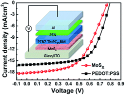
Here we employed a simple solution-processed method to prepare MoSx films as hole-transport layers (HTLs) in polymer solar cells (PSCs). Impressive performance was achieved with a power conversion efficiency (PCE) of 7.50%, which is comparable to those of the conventional devices with PEDOT:PSS HTLs. The surface and optoelectronic characteristics of MoSx films obtained from different conditions were investigated. The results reveal that the annealing temperature of MoSx is one of the most important factors on determining the device performance. PSCs based on MoSx films exhibited much better device stability compared to the counterpart based on PEDOT:PSS, suggesting that the MoSx film is a promising alternative HTL for PSCs.
Introduction
Polymer solar cells (PSCs) have attracted increasing attention in the past decade, and significant breakthroughs in power conversion efficiencies (PCEs) have been achieved through extensive efforts from material design to device engineering.1–4 Compared to the inorganic counterparts, PSCs have the advantages of low cost, light weight and good flexibility. In addition, organic materials are soluble in common organic solvents, and thus the roll-to-roll process at low cost can be used to make large area devices.5 In PSCs, interfaces between bulk heterojunctions (BHJs) and electrodes greatly affect the charge extraction and transport processes. Also, the bottom interface may influence the film morphology of the BHJs.6 As a result, interface engineering plays an important role on the device performance of PSCs.
In conventional PSCs the conducting polymer, poly(3,4-ethylenedioxythiophene):poly(styrenesulfonate) (PEDOT:PSS), is widely used to modify the work function (WF) of the indium tin oxide (ITO) as an efficient hole-transport layer (HTL). PEDOT:PSS has good optical transparency and an appropriate WF of ∼5.1 eV which makes it easy to form good ohmic contact at the electrode/BHJ interlayer.7 Thus, PSCs with PEDOT:PSS buffer layers have shown good performance, however, the devices are relatively unstable owning to the possible reactions between the PEDOT:PSS and the electrode caused by its acidity and hygroscopic nature.8,9 On the other hand, the electron leakage at the anode with PEDOT:PSS has been revealed to be another disadvantage.10 To overcome these defects, transition metal oxides have been investigated as efficient hole-transport materials to substitute PEDOT:PSS, such as V2O5, NiOx, WO3, and MoO3.11–14 For example, PSCs with high PCEs and good stability have been fabricated by using solution-processed MoO3 films due to their good morphological and electronic properties.15–17 Meanwhile, transition metal sulfides such as MoS2, WS2, and CuS have also come into sight due to their unique electrical properties and two-dimensional (2D) laminated structures.18–21
With improved hole extraction and transport properties, MoS2 films are usually fabricated as HTLs by a lithium intercalation and exfoliation process, which needs a relatively complicated procedure or other additional treatments.22–26 Alternatively, MoSx films can be prepared through a solution-processed method,27 which is more promising for large-scale production of organic solar cells. However, only few reports have been focused on solution-processed MoSx films for PSCs, and the highest PCE achieved so far is merely 3.90% based on the active layer of poly(3-hexylthiophene) and [6,6]phenyl-C61-butyric acid methyl ester (P3HT
:
PC61BM). As a universal hole-transport material, solution-processed MoSx films can be incorporated into other active layer systems for PSCs with better device performance. At the same time, it is worth to investigate the relationship between the structure of MoSx film and the performance of the resulting PSCs.
In this work, MoSx films were fabricated by spin-coating the MoSx precursor solution onto ITO/glass substrates with an annealing in air. The device configuration is shown in Fig. 1, where the active layer is based on a blend of poly[4,8-bis(5-(2-ethylhexyl)thiophen-2-yl)benzo[1,2-b:4,5-b′]dithiophene-co-3-fluorothieno[3,4-b]thiophene-2-carboxylate] (PTB7-Th) and [6,6]-phenyl-C71-butyric acid methyl ester (PC71BM). Conventional devices with PEDOT:PSS as HTLs were also fabricated by the same experimental condition for comparison.
 |
| Fig. 1 Schematic illustration of device configuration and molecular structures of PTB7-Th and PC71BM. | |
The annealing temperature of MoSx films significantly influenced the device performance, which may be ascribed to the modified interlayer characteristics (the annealing time is also an important factor as shown in Fig. S1†). Through optimization, the MoSx-based PSCs showed an impressive PCE of 7.50%, which approached the PCE of PEDOT:PSS-based device (8.00%). It is worth mentioning that the device based on MoSx was demonstrated to be more stable than that based on PEDOT:PSS.
Experimental section
Materials
(NH4)2MoS4 obtained from Alfa Aesar was used to prepare MoSx precursor solution. PTB7-Th was synthesized in our lab according to the published method1 and PC71BM was purchased from American Dye Source Inc. Other materials and reagents were purchased from Sigma-Aldrich Inc., Aladdin-Reagent Inc. or Adamas-beta Ltd. and used without further purification.
Preparation and characterization of MoSx films
A sol–gel process was used to fabricate MoSx films. To prepare the MoSx precursor solution, (NH4)2MoS4 was dissolved in deionized water with a concentration of 12 mg mL−1, and then stirred at 60 °C in a nitrogen atmosphere. The ITO/glass substrates were cleaned by sequentially ultrasonication in detergent, deionized water, acetone, and isopropyl alcohol for 30 min each and then dried at 80 °C overnight. The precursor films were prepared by spin-coating the (NH4)2MoS4 solution at 1200 rpm for 90 s on the ITO/glass substrates, after pretreating the substrates by UV-ozone for 15 min. Then the films were annealed at various temperatures (200, 250 and 300 °C) for 60 min in air and transferred into a N2-filled glovebox directly.
UV-vis absorption and transmission measurements were recorded by a Lambda35 spectrophotometer at room temperature. The film thicknesses were determined by a Bruker Dektak XT surface profiler. Atomic force microscopy (AFM) images were performed in air by using a Bruker Nanoscope 8.15 atomic force microscope. X-ray photoelectron spectroscopy (XPS) and ultraviolet photoelectron spectroscopy (UPS) were used for surface chemical analysis through a Thermo Scientific ESCALAB 250Xi XPS/UPS system with a monochromatic Al Kα source. The samples were tested after argon-ion etching for 30 s on the surfaces.
Hole-only devices (ITO/MoSx/PTB7-Th
:
PC71BM/Au) were fabricated to estimate the hole-transport property of MoSx films by the space charge limited current (SCLC) method. The hole mobilities were calculated by the equation:28 J = 9ε0εrμV2/8L3, where ε0 is the permittivity of free space, εr is the dielectric constant of the materials, μ is the hole mobility, V is the voltage drop across the device (V = Vapp − Vbi − Vr, where Vapp is the applied voltage to the device, Vbi is the built-in voltage due to the difference in WF of the two electrodes, Vr is the voltage drop due to contact resistance and series resistance across the electrodes), L is the thickness of the organic film.
Device fabrication and measurements
PSCs were fabricated with various MoSx films as the HTLs. PTB7-Th and PC71BM with a 1
:
1.5 w/w ratio were dissolved together in a mixed solvent of chlorobenzene and 1,8-diiodooctane (100
:
3 by volume) to give an overall 25 mg mL−1 solution. The active layer was fabricated in the glovebox by spin-coating the BHJ blend of PTB7-Th
:
PC71BM on the MoSx film. Then, the conjugated polymer poly[(9,9-bis(3′-(N,N-dimethylamino)propyl)-2,7-fluorene)-alt-2,7-(9,9-dioctylfluorene)] (PFN)29 was dissolved in methanol with a small amount of acetic acid (6 mg mL−1) to make a 0.3 mg mL−1 solution, and spin-coated onto the active layer at 1500 rpm for 30 s as cathode modification layer.30 Finally, the devices were transferred into a vacuum chamber and 100 nm of aluminum was deposited through shadow masks by thermal evaporation under a vacuum of ∼5 × 10⁻⁵ Pa. The effective area of the device was 4 mm2. Solar cell characterization was performed under AM 1.5G irradiation (100 mW cm−2) by an Oriel Sol3A simulator (Newport) with a NREL-certified silicon reference cell. After the device encapsulation, the current density–voltage (J–V) characteristics were measured by a Keithley 2440 source measurement unit. The EQE spectra were measured by a Newport EQE measuring system.
Results and discussion
Chemical analysis of MoSx films
To study the surface chemical states of MoSx, we performed XPS measurements. The samples on ITO/glass substrates were tested after surface cleaning. The photoelectron binding energy scale was calibrated to the C 1s peak for the C–C bonds at 284.8 eV. After fitting by Gaussian–Lorentzian curves, the Mo 3d XPS spectra of MoSx films obtained at different annealing temperatures are shown in Fig. 2. The relative contents of different valence states of molybdenum are estimated from the cover of the Gaussian curves. For the MoSx film obtained at 200 °C (Fig. 2a), the Mo 3d spectrum is fitted to the doublet peaks at 229.0 eV and 232.2 eV, corresponding to the Mo4+ peaks, and the doublet peaks at 231.2 eV and 234.4 eV, corresponding to the Mo5+ peaks. The peak at 226.2 eV belongs to the S 2s peak. The results reveal that two molybdenum oxidation states coexist in the film (31.28% Mo4+, 68.72% Mo5+). According to the literature,31 the spin–orbit doublet peaks at 228.8 eV and 231.9 eV belong to MoS2. Our results show that the binding energy of Mo4+ increased about 0.2 eV. Because the MoSx samples had been stored in air for a couple of days before XPS measurements, the presence of Mo5+ peaks may be ascribed to the partial oxidization of Mo from Mo4+ to Mo5+. This may also lead to a higher defect density and increase the binding energy. No prominent peak belongs to Mo6+ at about 236 eV can be observed, which proves that the MoSx films haven't been oxidized to MoO3.
 |
| Fig. 2 XPS spectra of the Mo 3d and S 2s core level peaks for MoSx films obtained at (a) 200, (b) 250, (c) 300 °C. (d) S 2p peaks for different annealing temperatures. | |
For the MoSx film obtained at 250 °C (Fig. 2b), the Mo 3d spectrum is fitted to the doublet peaks at 229.8 eV and 233.0 eV, corresponding to the Mo4+ peaks, and the doublet peaks at 231.7 eV and 234.9 eV, corresponding to the Mo5+ peaks. The peak at 226.4 eV belongs to the S 2s peak. The contents of Mo4+ and Mo5+ are 30.11% and 69.89%, respectively.
At 300 °C (Fig. 2c), the film component is 32.51% Mo4+ with doublet peaks at 229.5 eV and 232.7 eV, and 67.49% Mo5+ with doublet peaks at 231.2 eV and 234.4 eV. The S 2s peak is fitted at 226.0 eV. The results of valence states, peak positions and relative contents of different MoSx films calculated from Mo 3d scan are summarized in Table S2.† At different annealing temperatures, we fabricated MoSx films with different components. The slightly changed peak positions may be caused by different degrees of oxidization, which increase the density of defects in the films. When the annealing temperature increases from 200 °C to 300 °C, the peaks of S 2p at about 162.0 eV were observed for all three samples (Fig. 2d), further verifying the presence of MoS2.31
We also measured MoSx films by UPS, as shown in Fig. 3a. WFs of MoSx films obtained at 200, 250, 300 °C are calculated to be 5.0, 5.1, 5.1 eV, respectively. In the literature, single-layered and undoped MoS2 film has a WF of 4.4–4.5 eV.23 The larger WF of MoSx film may be ascribed to the presence of Mo5+, which increases the binding energy. As a result, the WF of MoSx matches well with the HOMO of PTB7-Th (5.22 eV), which reduces the energy barrier between the active layer and the ITO anode, as illustrated in the flat energy band diagram (Fig. 3b). The relative increased WFs of MoSx obtained at higher temperatures promote hole extraction and transport process, and improve the device performance.
 |
| Fig. 3 (a) UPS spectra of MoSx films on ITO/glass substrates obtained at different temperatures. (b) Flat energy band diagram of the components used in the PSCs. | |
Surface morphology of MoSx films
Since the device performance can be immensely influenced by the surface morphology of the interlayer, we further studied the surface characteristics of MoSx films by AFM. Fig. 4 shows the height images, three-dimensional (3D) surface topography images and surface profiles of MoSx films (on ITO substrates) obtained at different annealing temperatures. The bare ITO surface image was also captured as a comparison. The ITO shows a relatively rough surface with a root-mean-square (RMS) roughness of 0.66 nm, while the roughness of the MoSx film obtained at 300 °C is only 0.50 nm. Different from the ITO with a regularly arranged morphology, the MoSx films exhibit undulating topographies and smoother surfaces, which promote better interface contact and reduce the surface defects. The MoSx film processed at 200 °C shows a smaller particle packing surface, while those processed at higher temperatures show a sheet stacked surface. The special morphology of MoSx obtained at 200 °C may affect the electrical properties of the interface and the ohmic contact with the active layer, leading to the poor device performance.
 |
| Fig. 4 Tapping-mode AFM images of MoSx films on ITO and bare ITO surface, including height images, 3D topography images and surface profiles of (a) bare ITO (b) 200 °C MoSx (c) 250 °C MoSx (d) 300 °C MoSx. | |
Optical transmittance spectra of bare ITO and ITO/MoSx films are depicted in Fig. 5. High optical transparency can be observed in the visible region. Although MoSx films fabricated at different annealing temperatures exhibit some differences in film characteristics, they show similar optical transparencies.
 |
| Fig. 5 Linear transmission spectra of MoSx films obtained at different temperatures. | |
Device performance
Fig. 6a shows the J–V characteristics under AM 1.5G irradiation (100 mW cm−2). The PCEs of devices with MoSx HTLs obtained at different annealing temperatures show great difference. For the device with MoSx film obtained at 200 °C, the PCE is only 3.55%. The poor performance can be ascribed to the low open-circuit voltage (Voc) of 0.55 V, short-circuit current density (Jsc) of 16.36 mA cm−2 and fill factor (FF) of 39.21%. The device performance is improved as the annealing temperature increased from 200 °C to 300 °C. For the device with MoSx film obtained at 300 °C, the PCE is significantly improved to 7.50%, with increased Voc (0.77 V), Jsc (18.16 mA cm−2) and FF (53.56%). The improved device performance is mainly due to the modified interface characteristics between the ITO and active layer, which avoid the direct contact and enhance the charge extraction and transport processes. As the annealing temperature increased from 200 to 300 °C, reduced series resistance (Rs) and increased shunt resistance (Rsh) of the device were observed which is in agreement with the improved charge-transport process for the device with high temperature annealed MoSx. The high PCE is close to that of PEDOT:PSS-based devices fabricated in the same experimental condition for comparison (8.00%). The results are summarized in Table 1. Compared to the PEDOT:PSS-based device, a significantly increased Jsc is achieved for the MoSx-based device. The PCE distribution of devices with MoSx obtained at 300 °C is depicted in Fig. S2.†
 |
| Fig. 6 (a) J–V characteristics of PSCs with MoSx obtained at different temperatures and PEDOT:PSS as HTLs and (b) the corresponding EQE spectra (hollow symbols are the integrated photocurrents with the AM 1.5G spectrum). | |
Table 1 Device characteristics of PSCs with MoSx HTLs (obtained at 200, 250, 300 °C) and PEDOT:PSS HTLs
HTL |
Voc (V) |
Jsc (mA cm−2) |
FF (%) |
PCEmaxa (%) |
Rs (Ω cm2) |
Rsh (Ω cm2) |
The data in parentheses represent average PCEs obtained from eight devices. The Rs and Rsh were calculated by the inverse of the slope of the corresponding J–V curves under illumination at J = 0 and V = 0, respectively. |
MoSx 200 °C |
0.55 |
16.36 |
39.21 |
3.55 (3.14 ± 0.25) |
19.65 |
207.49 |
MoSx 250 °C |
0.64 |
16.89 |
35.65 |
3.86 (3.72 ± 0.11) |
35.08 |
257.59 |
MoSx 300 °C |
0.77 |
18.16 |
53.56 |
7.50 (7.36 ± 0.11) |
14.11 |
491.90 |
PEDOT:PSS |
0.79 |
16.05 |
62.70 |
8.00 (7.84 ± 0.15) |
9.69 |
773.36 |
The corresponding EQE spectra of PSCs incorporating MoSx and PEDOT:PSS are shown in Fig. 6b. High EQEs across the visible region can be observed for devices with MoSx HTLs. The MoSx-based device (300 °C) shows obviously higher EQEs especially from 450 to 600 nm compared to those of the PEDOT:PSS-based device. Integrating the EQE data with the AM 1.5G spectrum, we achieve the Jsc of 16.10, 16.60, 17.74, and 15.94 mA cm−2 for devices with MoSx obtained at 200, 250, 300 °C and PEDOT:PSS, respectively. Calculated Jsc values show less than 3% error compared to the measured values in Table 1.
The hole-transport abilities of MoSx and PEDOT:PSS films were studied by the SCLC method. From J–V characteristics of the hole-only devices (Fig. 7), hole mobilities of devices with MoSx obtained at 200, 250, 300 °C and PEDOT:PSS are estimated to be 4.52 × 10⁻⁶, 1.14 × 10⁻⁵, 5.97 × 10⁻⁵, and 2.63 × 10⁻⁵ cm2 V−1 s−1, respectively (the thicknesses of active layers are measured to be about 128, 144, 168, and 137 nm, respectively). The much higher hole mobility of MoSx obtained at 300 °C, even higher than PEDOT:PSS, may contribute to the better photovoltaic performance of the resulting device (Table 1).
 |
| Fig. 7 (a) J–V characteristics in the dark for hole-only devices with MoSx and PEDOT:PSS HTLs; (b) the corresponding J0.5–V characteristics. The solid lines are fits of the data points. | |
Device stability
Device stability also plays a key role in PSCs. To study the long-term stability of the devices with MoSx, the normalized PCEs as a function of storage time in air are depicted in Fig. 8. The device with MoSx HTL showed much better stability than the device with PEDOT:PSS HTL. After encapsulation, PEDOT:PSS exhibited a large degradation in three weeks. And after five weeks, only 13% of its original PCE value maintained. However, the device with MoSx was more stable. Even after two months, the device with MoSx still remained more than 52% of the initial efficiency. As a result, using MoSx to substitute PEDOT:PSS as HTL in conventional PSCs is proved to be an effective strategy to improve the long-term device stability.
 |
| Fig. 8 Device stability of PSCs with MoSx or PEDOT:PSS. | |
Conclusion
In summary, MoSx films were fabricated as HTLs for PSCs by a simple solution-processed method and their characteristics were examined. XPS analysis illustrated that MoSx films consisted of multiple valence states with Mo4+ and Mo5+. PSCs incorporating MoSx HTLs showed good performance with a highest PCE of 7.50%, which is close to those of the traditional devices with PEDOT:PSS HTLs. The results showed that the photovoltaic properties of MoSx films significantly depended on their annealing temperature. All of the photovoltaic parameters were improved as the annealing temperature increased from 200 to 300 °C, which can be attributed to the smoother surface, higher mobility, and a proper WF of 5.1 eV. Additionally, the MoSx-based device remained more than 50% of the initial PCE value even after two months, which was much more stable than the PEDOT:PSS-based conventional device. In general, this study demonstrates that solution-processed MoSx films are promising HTLs for high performance and stable PSCs.
Acknowledgements
This work was supported by the National Natural Science Foundation of China (NOs. 61325026 and 51173186), and the CAS/SAFEA International Partnership Program for Creative Research Teams.
Notes and references
- S.-H. Liao, H.-J. Jhuo, Y.-S. Cheng and S.-A. Chen, Adv. Mater., 2013, 25, 4766 CrossRef CAS PubMed.
- J. You, L. Dou, K. Yoshimura, T. Kato, K. Ohya, T. Moriarty, K. Emery, C.-C. Chen, J. Gao, G. Li and Y. Yang, Nat. Commun., 2013, 4, 1446 CrossRef PubMed.
- Y. Liu, J. Zhao, Z. Li, C. Mu, W. Ma, H. Hu, K. Jiang, H. Lin, H. Ade and H. Yan, Nat. Commun., 2014, 5, 5293 CrossRef CAS PubMed.
- S.-H. Liao, H.-J. Jhuo, P.-N. Yeh, Y.-S. Cheng, Y.-L. Li, Y.-H. Lee, S. Sharma and S.-A. Chen, Sci. Rep., 2014, 4, 6813 CrossRef CAS PubMed.
- F. He and L. Yu, J. Phys. Chem. Lett., 2011, 2, 3102 CrossRef CAS.
-
(a) L.-M. Chen, Z. Xu, Z. Hong and Y. Yang, J. Mater. Chem., 2010, 20, 2575 RSC;
(b) Z. Yin, J. Wei and Q. Zheng, Adv. Sci., 2016 DOI:10.1002/advs.201500362.
- H.-L. Yip and A. K. Y. Jen, Energy Environ. Sci., 2012, 5, 5994 CAS.
- Y.-H. Kim, S.-H. Lee, J. Noh and S.-H. Han, Thin Solid Films, 2006, 510, 305 CrossRef CAS.
- M. P. de Jong, L. J. van Ijzendoorn and M. J. A. de Voigt, Appl. Phys. Lett., 2000, 77, 2255 CrossRef CAS.
- H. Yan, P. Lee, N. R. Armstrong, A. Graham, G. A. Evmenenko, P. Dutta and T. J. Marks, J. Am. Chem. Soc., 2005, 127, 3172 CrossRef CAS PubMed.
- X. Bao, Q. Zhu, T. Wang, J. Guo, C. Yang, D. Yu, N. Wang, W. Chen and R. Yang, ACS Appl. Mater. Interfaces, 2015, 7, 7613 CAS.
- F. Jiang, W. C. H. Choy, X. Li, D. Zhang and J. Cheng, Adv. Mater., 2015, 27, 2930 CrossRef CAS PubMed.
- M. Vasilopoulou, A. Soultati, D. G. Georgiadou, T. Stergiopoulos, L. C. Palilis, S. Kennou, N. A. Stathopoulos, D. Davazoglou and P. Argitis, J. Mater. Chem. A, 2014, 2, 1738 CAS.
- Z. A. Tan, D. Qian, W. Zhang, L. Li, Y. Ding, Q. Xu, F. Wang and Y. Li, J. Mater. Chem. A, 2013, 1, 657 CAS.
- J. J. Jasieniak, J. Seifter, J. Jo, T. Mates and A. J. Heeger, Adv. Funct. Mater., 2012, 22, 2594 CrossRef CAS.
- B. J. Tremolet de Villers, R. C. I. MacKenzie, J. J. Jasieniak, N. D. Treat and M. L. Chabinyc, Adv. Energy Mater., 2014, 4, 1301290 Search PubMed.
- Q. Yi, P. Zhai, Y. Sun, Y. Lou, J. Zhao, B. Sun, B. Patterson, H. Luo, W. Zhang, L. Jiao, H. Wang and G. Zou, ACS Appl. Mater. Interfaces, 2015, 7, 18218 CAS.
- P. Qin, G. Fang, W. Ke, F. Cheng, Q. Zheng, J. Wan, H. Lei and X. Zhao, J. Mater. Chem. A, 2014, 2, 2742 CAS.
- J.-M. Yun, Y.-J. Noh, C.-H. Lee, S.-I. Na, S. Lee, S. M. Jo, H.-I. Joh and D.-Y. Kim, Small, 2014, 10, 2319 CrossRef CAS PubMed.
- Q. V. Le, T. P. Nguyen and S. Y. Kim, Phys. Status Solidi RRL, 2014, 8, 390 CrossRef CAS.
- H. Lei, G. Fang, F. Cheng, W. Ke, P. Qin, Z. Song, Q. Zheng, X. Fan, H. Huang and X. Zhao, Sol. Energy Mater. Sol. Cells, 2014, 128, 77 CrossRef CAS.
- G. L. Frey, K. J. Reynolds, R. H. Friend, H. Cohen and Y. Feldman, J. Am. Chem. Soc., 2003, 125, 5998 CrossRef CAS PubMed.
- J.-M. Yun, Y.-J. Noh, J.-S. Yeo, Y.-J. Go, S.-I. Na, H.-G. Jeong, J. Kim, S. Lee, S.-S. Kim, H. Y. Koo, T.-W. Kim and D.-Y. Kim, J. Mater. Chem. C, 2013, 1, 3777 RSC.
- X. Yang, W. Fu, W. Liu, J. Hong, Y. Cai, C. Jin, M. Xu, H. Wang, D. Yang and H. Chen, J. Mater. Chem. A, 2014, 2, 7727 CAS.
- D. J. Finn, M. Lotya, G. Cunningham, R. J. Smith, D. McCloskey, J. F. Donegan and J. N. Coleman, J. Mater. Chem. C, 2014, 2, 925 RSC.
- X. Gu, W. Cui, H. Li, Z. Wu, Z. Zeng, S.-T. Lee, H. Zhang and B. Sun, Adv. Energy Mater., 2013, 3, 1262 CrossRef CAS.
- X. Li, W. Zhang, Y. Wu, C. Min and J. Fang, ACS Appl. Mater. Interfaces, 2013, 5, 8823 CAS.
- G. G. Malliaras, J. R. Salem, P. J. Brock and C. Scott, Phys. Rev. B: Condens. Matter Mater. Phys., 1998, 58, R13411 CrossRef CAS.
- Z. He, C. Zhong, S. Su, M. Xu, H. Wu and Y. Cao, Nat. Photonics, 2012, 6, 591 Search PubMed.
- L. Zhang, C. He, J. Chen, P. Yuan, L. Huang, C. Zhang, W. Cai, Z. Liu and Y. Cao, Macromolecules, 2010, 43, 9771 CrossRef CAS.
- C. D. Wagner, W. M. Riggs, L. E. Davis and J. F. Moulder, Handbook of X-ray Photoelectron Spectroscopy, ed. G. E. Muilenberg, Perkin-Elmer Corporation, Eden Prairie, 1979 Search PubMed.
Footnote |
† Electronic supplementary information (ESI) available: The PCE distribution of devices with MoSx obtained at 300 °C, summary of XPS analysis calculated from Mo 3d scan and device performance of different experimental conditions. See DOI: 10.1039/c6ra01204c |
|
This journal is © The Royal Society of Chemistry 2016 |
Click here to see how this site uses Cookies. View our privacy policy here.