Electrodeposition of Prussian blue films on Ni3Si2O5(OH)4 hollow nanospheres and their enhanced electrochromic properties

Tailiang Lia, Congcong Zhaoab, Dongyun Maa, Fanglin Dub and Jinmin Wang*a
aSchool of Environmental and Materials Engineering, College of Engineering, Shanghai Second Polytechnic University, Shanghai 201209, China. E-mail: wangjinmin@sspu.edu.cn; Fax: +86-21 50217725; Tel: +86-21 50217725
bCollege of Materials Science and Engineering, Qingdao University of Science and Technology, Qingdao 266042, China

Received 12th January 2016 , Accepted 6th April 2016

First published on 7th April 2016


Abstract

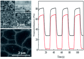
Porous Prussian blue (PB) films were successfully electrodeposited on Ni3Si2O5(OH)4 hollow nanosphere coated indium tin oxide (ITO) glass. Ni3Si2O5(OH)4 hollow nanospheres hydrothermally synthesized using SiO2 nanospheres as templates play a key role in the formation of porous PB films. The as-prepared PB films exhibit larger transmittance change, faster switching response and higher coloration efficiency than those of dense PB films directly electrodeposited on ITO glass. The enhanced electrochromic properties are attributed to the large specific surface area and porosity of the PB films which bring a high diffusion rate and short diffusion path length of ions.


Introduction

Electrochromic materials exhibit reversible changes in optical properties under the action of an applied voltage.1 The change in transmittance or reflectance is usually associated with the change of color.2,3 Electrochromic materials can be applied in smart windows, anti-dazzling rear-view mirrors and other aspects.4,5 An electrochromic material may exhibit only one color change commonly between bleached and coloration states, or two or more color changes unless where two or more redox states are electrochemically available.6,7 Prussian blue (PB) is an interesting material due to its excellent magnetic and electrochemical properties.8,9 PB can be deposited on a conductive substrate from a precursor solution by applying a current or voltage.10 Neff studied the deposition of PB film on Pt or Au substrates in a solution containing hexacyanoferrate and ferric chloride.11 However, this kind of PB film with a dense surface is usually against to the injection and extraction of ions. Therefore, the modification of PB films has attracted a great attention and interest.12–17 The electrochromic properties of PB films have also been studied, due to their color changes between Prussian white (PW), PB and Prussian green (PG).18,19

Electrochromism of inorganic materials is due to the reversible injection and extraction of ions and electrons. The kinetics and degree of ions injection and extraction have a great relation to the surface morphology and microstructure of PB films.20 To obtain better electrochromic properties, electrochromic films with large specific surface area and porosity are desired.21–23

Hollow nanostructures provide high specific surface areas, which facilitate the sufficiently large contact of ions. Moreover, the hollow interior structures afford a large free volume for storage capacity. Therefore, hollow nanostructures have aroused great attention in the past few years, and many related works have been reported.24 Such as PB hollow nanostructures,25,26 FeCo2O4 hollow nanospheres,27 Fe2O3@polyaniline hollow nanospheres,28 WO3 hollow nanospheres,29 V2O5 hollow nanospheres30 and nickel silicate hollow sphere.31 Specifically, Zhu et al.32 reported uniform and hierarchical NiS hollow spheres with a diameter of 400 nm using a template-engaged conversion method. The NiS hollow spheres show enhanced electrochemical properties as electrode materials for supercapacitors. Guo et al.33 successfully synthesized Ni3Si2O5(OH)4 hollow nanospheres using a simple self-template approach. The diameter of hollow nanospheres is about 300 nm, and the specific surface area is about 190 m2 g−1. As described above, there are many advantages for hollow nanospheres. However, there is no report on the electrodeposition of electrochromic films using hollow nanospheres.

In this work, we provide a simple method for the preparation of Ni3Si2O5(OH)4 hollow nanospheres. Moreover, we present a new approach to deposite PB films on rough hollow nanospheres instead of on smooth indium tin oxide (ITO) glass. Compared with dense PB films directly deposited on ITO glass, enhanced transmittance change, switching response and coloration efficiency are achieved for the PB films deposited on hollow nanospheres.

Experimental section

Films preparation

All reagents were analytical grade without further purification, purchased from Sinopharm Chemical Reagent Co., Ltd (China). The specifications of ITO glass used in this work are described below: square resistance ≤ 15 Ω, transmittance ≥ 84% in the wavelength range of 500 to 800 nm.

Firstly, SiO2 nanospheres were prepared as follows: in a typical synthesis, 16.0 mL of ethanol, 25.0 mL of de-ionized water, and 7.0 mL of ammonia solution (28–30 wt%) were added into a round-bottom flask. After stirring for 10 min at 40 °C, a mixed solution containing 45.5 mL of ethanol and 4.5 mL of tetraethylorthosilicate (TEOS) was rapidly added into the round-bottom flask, and then stirred for 8 h. SiO2 nanospheres were obtained after centrifugation and washed repeatedly by deionized water and ethanol to remove possible impurities, followed by vacuum drying at 80 °C overnight. Secondly, Ni3Si2O5(OH)4 hollow nanospheres were prepared as follows: 1.0 g of SiO2 nanospheres, 1.0 g of urea and 0.2 g of Ni(NO3)2·6H2O were dissolved in 40 mL of de-ionized water with ultrasonication before being transferred into a Teflon-lined autoclave. Then, the autoclave was heated at 105 °C for 12 h. After natural cooling to room temperature, SiO2@Ni3Si2O5(OH)4 composite nanospheres were obtained after being centrifuged, washed and dried. A 40 mL of solution containing 0.1 g of SiO2@Ni3Si2O5(OH)4 composite nanospheres was prepared after adjusting the pH value of the solution to 13, using saturated NaOH solution. Then, the solution was transferred into a Teflon-lined autoclave with a 50 mL of capacity and maintained at 160 °C for 12 h. The product was centrifuged, washed with de-ionized water. After being dried in a vacuum oven at 60 °C for 12 h, Ni3Si2O5(OH)4 hollow nanospheres were obtained.

ITO-coated glasses (20 mm × 40 mm in size) were cleaned by ultrasonication in acetone, ethanol and de-ionized water for 15 min, respectively. By dispersing 0.1 g of Ni3Si2O5(OH)4 hollow nanospheres in 10 mL of ethanol, and then spin-coating the solution on ITO glasses for three times, rough substrates containing hollow nanospheres were prepared. PB films were electrodeposited using our previously reported method.34 A mixed aqueous solution containing 10 mmol L−1 of K3[Fe(CN)]6, 10 mmol L−1 of FeCl3 and 50 mmol L−1 of KCl was used as the electrolyte. The as-prepared rough substrate coated on ITO glass was used as the working electrode, Ag/AgCl reference electrode and Pt sheet counter electrode were also used. PB films were deposited under a constant current density of −50 μA cm−2 for 300 s. For comparison, PB films were also electrodeposited on bare ITO glasses under the same conditions. PB film electrodeposited on Ni3Si2O5(OH)4 hollow nanospheres is named as PB with coating, and the film deposited directly on ITO glass is named as PB without coating. After electrodeposition, the films were washed with ethanol to remove the remaining electrolyte, and then dried at room temperature before characterizations and electrochromic measurements.

Characterizations

The phase identification of the samples was characterized by X-ray diffraction (XRD, Cu Kα radiation, λ = 0.15418 nm), the morphology of the as-synthesized samples were examined with field emission scanning electron microscopy (FESEM, 10 kV, 10 μA) and transmission electron microscopy (TEM, JEM 2100 F, 200 kV). The transmittance measurements of PB films were carried out using an UV-Vis spectrophotometer (PC SHIMADZU, UV 2600, Japan) over the wavelength range from 400 to 800 nm at room temperature (optical response was measured at λ = 700 nm). The electrochromic properties of PB films were conducted on an Autolab electrochemical workstation with a conventional three-electrode system comprising PB film as the working electrode, Pt sheet as the counter electrode and Ag/AgCl as the reference electrode, 1.0 mol L−1 of KCl as the electrolyte. The cyclic coloration and bleaching were tested by applying 0.7 V for 15 s and −0.6 V for 15 s, respectively. Cyclic voltammograms (CVs) were measured from −0.6 to 1.70 V with a scanning rate of 0.1 V s−1.

Results and discussion

Structure and morphology

The XRD patterns of SiO2 nanospheres and Ni3Si2O5(OH)4 hollow nanospheres are shown in Fig. 1. The broad peak in the XRD pattern of SiO2 nanospheres (Fig. 1a) corresponds to amorphous structure of SiO2. All peaks in Fig. 1b are well indexed to the standard diffraction peaks of Ni3Si2O5(OH)4 (JCPDS no. 49-1859), which indicates that SiO2 nanospheres have been completely etched by NaOH.
image file: c6ra00967k-f1.tif
Fig. 1 XRD patterns of (a) SiO2 nanospheres and (b) Ni3Si2O5(OH)4 hollow nanospheres.

Fig. 2 shows the morphological changes from SiO2 nanospheres to Ni3Si2O5(OH)4 hollow nanospheres of the samples. As shown in Fig. 2a, the SiO2 nanospheres is ∼120–130 nm in diameter, which can be adsorbed by Ni2+ ions during hydrothermal process because of the negative groups on the surface of nanospheres. With the decomposition of urea to ammonia and the hydrolysis of ammonia, the solution became alkaline, resulting in the formation of silicate ions on the surface of SiO2 nanospheres. Then, Ni3Si2O5(OH)4 was formed on the surface of SiO2 nanospheres due to the chemical reaction among Ni2+, OH and silicate ions. From Fig. 2b, it can be clearly seen that the SiO2 nanospheres are uniformly coated by Ni3Si2O5(OH)4 nanospheres, the diameter of SiO2@Ni3Si2O5(OH)4 nanospheres is ∼130–140 nm. Finally, after SiO2 nanospheres being etched by NaOH solution, the Ni3Si2O5(OH)4 hollow nanospheres were obtained, and the diameter is maintained at ∼130–140 nm. Fig. 2d–f show the TEM images of SiO2@Ni3Si2O5(OH)4 nanospheres and Ni3Si2O5(OH)4 hollow nanospheres. It can be seen that the surfaces of the SiO2@Ni3Si2O5(OH)4 nanospheres are sea urchin-like (Fig. 2d). After the removal of SiO2, the obtained Ni3Si2O5(OH)4 nanospheres form a hollow sea urchin-like structure with a shell thickness of few nanometers (Fig. 2e and f). The structure of hollow nanospheres has a large surface area, which is favorable for the injection and extraction of ions and electrons.35–38


image file: c6ra00967k-f2.tif
Fig. 2 FESEM images of (a) SiO2 nanospheres, (b) SiO2@Ni3Si2O5(OH)4 nanospheres, (c) Ni3Si2O5(OH)4 hollow nanospheres. TEM images of (d) SiO2@Ni3Si2O5(OH)4 composite, (e) and (f) Ni3Si2O5(OH)4 hollow nanospheres.

Compared with PB without coating (Fig. 3b), the surface of PB with coating is rough and porous, which benefits from pre-spin coated hollow nanospheres before electrodeposition. Due to the deposition process of PB, the diameter of hollow nanospheres is increased to ∼200 nm (Fig. 3a). This structure provides a larger surface area than the PB film with smooth and compact surface, which may lead to a fast injection/extraction of ions. As a result, enhanced electrochromic performances may be achieved. The change in morphology of PB with coating can be clearly observed by cross-sectional FESEM images (Fig. 3c and d). From bottom to top, the glass substrate, ITO layer and PB film can be clearly seen (Fig. 3c), and porous surface morphology that formed by the hollow nanospheres can also be easily observed. The thickness of PB with coating is ∼6 μm. Compared with the FESEM and TEM images shown in Fig. 2, it can be seen that there are large changes in structure and morphology of hollow nanospheres coated by PB (Fig. 3d). Moreover, flower-like nanosheets grown uniformly on surface of part nanospheres (Fig. 3d) may be caused by the folds and burrs that formed on the surface of hollow nanospheres (Fig. 2f). It is helpful to enhance the specific surface area of PB film.


image file: c6ra00967k-f3.tif
Fig. 3 FESEM images of PB films deposited with a current density of −50 μA cm−2 for 300 s: (a) top-view of PB with coating, (b) top-view of PB without coating, (c) cross-section of PB with coating and (d) magnified image of the area in (c).

Electrochromic properties

CV curves of two kinds of PB films are shown in Fig. 4. At the beginning of electrochemical cycle, the CV curve is not stable and actual. The potentials of oxidation and reduction peaks will be changed and migrated to both sides with increase of cycle number. This is due to the injection and extraction of electrons and ions are not complete at the initial stage. After a few cycles, the electrochemical reaction will reach a steady state finally. The transition metal oxide electrochromic materials have a single color change generally, while PB has more than one redox reaction. Therefore, it has more than one color change from oxidation state to reduction state. PB would be appeared when PW is partly oxidized; then PG will be appeared after PB being oxidized. Conversely, PW will be appeared after PG is reduced completely. As shown in Fig. 4, two kinds of PB films both have two couple of redox peaks. The oxidation peaks of PB without coating are at 0.83 and 1.46 V, reduction peaks are at 0.83 and 0.10 V, respectively. The oxidation peaks of PB with coating are at 0.96 and 1.67 V, and reduction peaks are at 0.63 and −0.15 V, respectively. The oxidation potential of PB with coating shifts to the right compared with PB without coating, while the reduction potential shifts to the left. This might be caused by the changes in film resistance. In comparison with the PB without coating, the PB with coating would give a greater resistance due to the poor conductivity of pre-coated Ni3Si2O5(OH)4 hollow nanospheres, and thus the redox peaks shift to the both sides.39,40
image file: c6ra00967k-f4.tif
Fig. 4 CV curves of (a) PB without coating and (b) PB with coating.

As shown in Fig. 5, after electrodeposition, the PB film presents an original blue color. After a potential of 0 V was applied as the scanning starting potential, the color of PB film changes from blue to colorless quickly, due to the reduction reaction caused by ions and electron injection (Fig. 5b). With the increase of potential from zero to positive range (0–0.96 V), the PB film with coating gradually changes from PW (colorless) to PB (Fig. 5b and c). As potential increases continuously (0.96–1.67 V), part of the PB is oxidized to PG (Fig. 5c and d). When the scanning potential gradually decreases (1.70–0.63 V), the PG is reduced to PB (Fig. 5d and e). As potential decreases continuously (0.63 to −0.60 V), PB is reduced to PW41,42 (Fig. 5e and b). The color change behavior is along with two redox couples according to the following reactions.43

 
KFeIII[FeII(CN)6](PB) + e + K+ = K2FeII[FeII(CN)6](PW) (1)
 
3KFeIII[FeII(CN)6](PB) = KFeIII3{[FeIII(CN)6]2[FeII(CN)6]}(PG) + 2e + 2K+ (2)


image file: c6ra00967k-f5.tif
Fig. 5 Color changes of PB with coating: (a) color of PB film after electrodeposition, (b) color of PB film at 0 V, (c) color of PB film at 0.7 V, (d) color of PB film at 1.6 V, (e) color of PB film at 0.6 V.

The transmittance modulation of PB films between the colored and bleached states is an important parameter of the electrochromic properties.44 Applying potentials of 0.7 and −0.6 V, the two kinds of films both presented colors of PB and PW. The corresponding transmittance changes were measured in the wavelength range of 400 to 800 nm and shown in Fig. 6. The maximum transmittance modulations of PB with and without coating at 700 nm were calculated to be 66.4% and 55.2%, respectively. Compared with the transmittance (82.4%) of PB without coating in bleached state, the PB with coating shows a lower transmittance (68.9%), which may be caused by the template layer of hollow nanospheres. However, the transmittance of PB with coating in colored state (2.5%) is much lower than that of PB without coating (27.2%). This should be attributed to the large surface area of PB with coating, which facilities the extraction of K+ ions. Compared with the PB without coating, more K+ ions are extracted under the same applied voltage within a certain period of time and the deeper color is obtained for the PB with coating. The coloration efficiency (CE) values of PB with coating and PB without coating can also indirectly support the result. Thus the PB with coating presents a better electrochromic effect than PB without coating.


image file: c6ra00967k-f6.tif
Fig. 6 Transmittance spectra of (a) PB without coating and (b) PB with coating measured at bleached states and colored states.

Another important aspect of electrochromic properties is the switching response under alternating potentials. The corresponding optical responses curves of two films measured at 700 nm are shown in Fig. 7. The switching times of both PB films were investigated at wavelength of 700 nm by the alternating potentials of −0.6 V and 0.7 V. The switching time is defined as the time required for 90% changes in the transmittance between the colored and bleached states. For PB with coating, the coloration time (from the bleached state to the colored state) tc is calculated to be 2.3 s, and the bleaching time (from the colored state to the bleached state) tb is 2.2 s, meanwhile the tc and tb of PB without coating are 3.4 and 2.3 s, respectively. The coloration time of PB with coating is shorter than that of PB without coating because the high-porosity nanostructure brings a high diffusion coefficient and short diffusion path length of ions.


image file: c6ra00967k-f7.tif
Fig. 7 Coloration/bleaching switching response curves of (a) PB without coating and (b) PB with coating.

CE is defined as the change in optical density (ΔOD) per unit of charge (ΔQ) intercalated into the electrochromic layers. It can be calculated according to the following formulas:

 
CE = ΔOD/(Q/A) (3)
 
ΔOD = log(tb)/(tc) (4)

Fig. 8 shows the optical density changes with respect to the charge densities of two films. The calculated CE values of PB with coating and PB without coating are 42.5 and 20.7 cm2 C−1, respectively. A higher value of CE indicates that a larger optical modulation is completed in the same time after voltage switching, or a major optical modulation is completed with smaller charge extraction. The higher CE value of PB with coating should be attributed to the higher porosity of the film, which brings a higher diffusion coefficient and shorter diffusion path length of ions.


image file: c6ra00967k-f8.tif
Fig. 8 Optical density changes with respect to the charge densities of (a) PB without coating and (b) PB with coating.

Conclusions

In summary, Ni3Si2O5(OH)4 hollow nanospheres have been synthesized and used as a rough substrate for electrodeposition of porous PB films with enhanced electrochromic properties. The results indicate that the structure and morphology have a great impact on the electrochromic performances of PB films. The porous PB film presents higher optical modulation (66.4% at 700 nm) than dense PB film (55.2% at 700 nm). Due to the porous structure leading to higher diffusion rate and shorter diffusion path length of ions, the porous PB film shows a faster switching response of 2.3 s for coloration and 2.2 s for bleaching, and a larger coloration efficiency of 42.5 cm2 C−1 than those (3.4 s for coloration, 2.3 s for bleaching, and 20.7 cm2 C−1 for coloration efficiency) of dense PB film. The developed deposition approach using hollow nanospheres may be extended to prepare other high-porosity films for a variety of applications.

Acknowledgements

We would like to thank support from National Natural Science Foundation of China (NSFC) (No. 61376009), the Program for Professor of Special Appointment (Eastern Scholar) at Shanghai Institutions of Higher Learning (No. 2013-70), “Shu Guang” project supported by Shanghai Municipal Education Commission and Shanghai Education Development Foundation (No. 13SG55), Graduate Program Fund supported by Shanghai Second Polytechnic University (A30NH1513016).

Notes and references

  1. A. Branco, L. C. Branco and F. Pina, Chem. Commun., 2011, 47, 2300–2302 RSC.
  2. H. Shin, S. Seo, C. Park, J. Na, M. Han and E. Kim, Energy Environ. Sci., 2016, 9, 117–122 CAS.
  3. H. Z. Li, J. W. Chen, M. Q. Cui, G. F. Cai, A. L.-S. Eh, P. S. Lee, H. Z. Wang, Q. H. Zhang and Y. G. Li, J. Mater. Chem. C, 2016, 4, 33–38 RSC.
  4. G. A. Niklasson and C. G. Granqvist, J. Mater. Chem., 2007, 17, 127–156 RSC.
  5. Q. L. Jiang, F. Q. Liu, T. Li and T. Xu, J. Mater. Chem. C, 2014, 2, 618–621 RSC.
  6. R. J. Mortimer and J. R. Reynolds, J. Mater. Chem., 2005, 15, 2226–2233 RSC.
  7. L. Han, L. Bai and S. J. Dong, Chem. Commun., 2014, 50, 802–804 RSC.
  8. S. A. M. Shaegh, N.-T. Nguyen, S. M. M. Ehteshami and S. H. Chan, Energy Environ. Sci., 2012, 5, 8225–8228 Search PubMed.
  9. E. Nossol and A. J. G. Zarbin, J. Mater. Chem., 2012, 22, 1824–1833 RSC.
  10. D. Zhang, K. Wang, D. C. Sun, X. H. Xia and H.-Y. Chen, Chem. Mater., 2003, 15, 4163–4165 CrossRef CAS.
  11. V. D. Neff, J. Electrochem. Soc., 1978, 125, 886–887 CrossRef CAS.
  12. G. S. Lai, H. L. Zhang, A. M. Yu and H. X. Ju, Biosens. Bioelectron., 2015, 74, 660–665 CrossRef CAS PubMed.
  13. S. Jana and A. Mondal, ACS Appl. Mater. Interfaces, 2014, 6, 15832–15840 CAS.
  14. X. X. Liu, A. W. Zhou, Y. B. Dou, T. Pan, M. F. Shao, J. B. Han and M. Wei, Nanoscale, 2015, 7, 17088–17095 RSC.
  15. D. D. Liana, B. Raguse, J. J. Gooding and E. Chow, ACS Appl. Mater. Interfaces, 2015, 7, 19201–19209 CAS.
  16. J. H. Ko, S. Yeo, J. H. Park, J. Choi, C. Noh and S. U. Son, Chem. Commun., 2012, 48, 3884–3886 RSC.
  17. X. L. Liang, Z. J. Deng, L. J. Jing, X. D. Li, Z. F. Dai, C. H. Li and M. M. Huang, Chem. Commun., 2013, 49, 11029–11031 RSC.
  18. C.-F. Lin, C.-Y. Hsu, H.-C. Lo, C.-L. Lin, L.-C. Chen and K.-C. Ho, Sol. Energy Mater. Sol. Cells, 2011, 95, 3074–3080 CrossRef CAS.
  19. S. S. Kumar, J. Joseph and K. L. Phani, Chem. Mater., 2007, 19, 4722–4730 CrossRef CAS.
  20. Y. C. Zhu, T. Mei, Y. Wang and Y. T. Qian, J. Mater. Chem., 2011, 21, 11457–11463 RSC.
  21. T.-D. Nguyen, C.-T. Dinh and T.-O. Do, Nanoscale, 2011, 3, 1861–1873 RSC.
  22. S. K. Yang, M. I. Lapsley, B. Q. Cao, C. L. Zhao, Y. H. Zhao, Q. Z. Hao, B. Kiraly, J. Scott, W. Z. Li, L. Wang, Y. Lei and T. J. Huang, Adv. Funct. Mater., 2013, 23, 720–730 CrossRef CAS.
  23. X.-H. Xia, J.-P. Tu, X.-L. Wang, C.-D. Guo and X.-B. Zhao, J. Mater. Chem., 2011, 21, 671–679 RSC.
  24. R. McHale, Y. B. Liu, N. Ghasdian, N. S. Hondow, S. J. Ye, Y. Lu, R. Brydson and X. S. Wang, Nanoscale, 2011, 3, 3685–3694 RSC.
  25. M. Hu, S. Furukawa, R. Ohtani, H. Sukegawa, Y. Nemoto, J. Reboul, S. Kitagawa and Y. Yamauchi, Angew. Chem., Int. Ed., 2012, 51, 984–988 CrossRef CAS PubMed.
  26. N. L. Torad, M. Hu, M. Imura, M. Naito and Y. Yamauchi, J. Mater. Chem., 2012, 22, 18261–18267 RSC.
  27. L. Liu, Z. B. Hu, L. M. Sun, G. Gao and X. F. Liu, RSC Adv., 2015, 5, 36575–36581 RSC.
  28. J.-M. Jeong, B. G. Choi, S. C. Lee, K. G. Lee, S.-J. Chang, Y.-K. Han, Y. B. Lee, H. U. Lee, S. Kwon, G. Lee, C.-S. Lee and Y. S. Huh, Adv. Mater., 2013, 25, 6250–6255 CrossRef CAS PubMed.
  29. M. Sasidharan, N. Gunawardhana, M. Yoshio and K. Nakashima, Nano Energy, 2012, 1, 503–508 CrossRef CAS.
  30. A. Q. Pan, T. Zhu, H. B. Wu and X. W. Lou, Chem.–Eur. J., 2013, 19, 494–500 CrossRef CAS PubMed.
  31. C. J. Tang, J. Z. Sheng, C. Xu, S. M. B. Khajehbashi, X. P. Wang, P. Hu, X. J. Wei, Q. L. Wei, L. Zhou and L. Q. Mai, J. Mater. Chem. A, 2015, 3, 19427–19432 CAS.
  32. T. Zhu, Z. Y. Wang, S. J. Ding, J. S. Chen and X. W. Lou, RSC Adv., 2011, 1, 397–400 RSC.
  33. Z. Y. Guo, F. L. Du, G. C. Li and Z. L. Cui, Chem. Commun., 2008, 2911–2913 RSC.
  34. J. M. Wang, L. Zhang, L. Yu, Z. H. Jiao, H. Q. Xie, X. W. Lou and X. W. Sun, Nat. Commun., 2014, 5, 4921 CrossRef CAS PubMed.
  35. G. Q. Zhang, H. B. Wu, T. Song, U. Paik and X. W. Lou, Angew. Chem., Int. Ed., 2014, 53, 12590–12593 CAS.
  36. S. J. Peng, L. L. Li, H. T. Tan, R. Cai, W. H. Shi, C. C. Li, S. G. Mhaisalkar, M. Srinivasan, S. Ramakrishna and Q. Y. Yan, Adv. Funct. Mater., 2014, 24, 2155–2162 CrossRef CAS.
  37. A. P. Vogt, J. D. Winter, P. Krolla-Sidenstein, U. Geckle, O. Coulembier and C. Bamer-Kowollik, J. Mater. Chem. B, 2014, 2, 3578–3581 RSC.
  38. K. D. Kelly and J. B. Schlenoff, ACS Appl. Mater. Interfaces, 2015, 7, 13980–13986 CAS.
  39. J. F. Qian, Y. Chen, L. Wu, Y. L. Cao, X. P. Ai and H. X. Yang, Chem. Commun., 2012, 48, 7070–7072 RSC.
  40. Y. L. Shao, H. Z. Wang, Q. H. Zhang and Y. G. Li, J. Mater. Chem. C, 2013, 1, 1245–1251 RSC.
  41. Z. H. Jiao, J. M. Wang, L. Ke, X. W. Liu, H. V. Demir, M. F. Yang and X. W. Sun, Electrochim. Acta, 2012, 63, 153–160 CrossRef CAS.
  42. S.-F. Hong and L.-C. Chen, Sol. Energy Mater. Sol. Cells, 2012, 104, 64–74 CrossRef CAS.
  43. D. M. DeLongchamp and P. T. Hammond, Adv. Funct. Mater., 2004, 14, 224–232 CrossRef CAS.
  44. R. Sydam, M. Deepa and A. K. Srivastava, RSC Adv., 2012, 2, 9011–9021 RSC.

This journal is © The Royal Society of Chemistry 2016
Click here to see how this site uses Cookies. View our privacy policy here.