
 Open Access Article
 This Open Access Article is licensed under a Creative Commons Attribution-Non Commercial 3.0 Unported Licence
Reliable resistive switching memory based on oxygen-vacancy-controlled bilayer structures†
Kyuhyun
Park
and
Jang-Sik
Lee
*
Department of Materials Science and Engineering, Pohang University of Science and Technology (POSTECH), Pohang 790-784, Korea. E-mail: jangsik@postech.ac.kr
First published on 16th February 2016
Abstract
We fabricated resistive random access memory (RRAM) devices composed of a bilayer of AlOx. The AlOx layer was synthesized by atomic layer deposition (ALD) with different oxidizer sources. To control the number of oxygen vacancies, we used water and ozone as the oxidizer sources in ALD. The AlOx layer synthesized using water as the oxidizer source (AlOx(water)) contained more oxygen vacancies than the AlOx layer deposited using ozone as the oxidizer (AlOx(ozone)). We fabricated memory devices with a structure of Al/AlOx(water)/AlOx(ozone)/Pt by ALD. After the initial forming process the devices showed reproducible and reliable RRAM characteristics. Bipolar resistive change was observed in Al/AlOx(water)/AlOx(ozone)/Pt RRAM devices with low operation voltages of less than 1 V. Ohmic conduction behavior was dominant in the low resistance state and trap-controlled space-charge-limited conduction was observed in the high resistance state. The resistive switching is related to migration of oxygen vacancies and the formation/rupture of conductive filaments. Oxygen vacancies formed conductive filaments when an electric field was applied, and Joule heating broke them. The reliability of the devices was confirmed by data retention and endurance tests. The reliable bipolar resistive switching properties are attributed to a stable conductive filament in the AlOx(water) layer and partial connection/disruption of a conductive filament localized at the AlOx(ozone) layer.
Introduction
Resistive random access memory (RRAM) is a promising candidate for next-generation non-volatile memory (NVM), which exploits the resistance change between high resistance state (HRS) and low resistance state (LRS). RRAM has advantages such as excellent cycling endurance, long-term retention, fast switching, low power consumption, and multistate behavior.1–9 Resistive switching behavior has been reported in various materials such as transition metal oxides, perovskites, metal halides, and chalcogenides.10 Recently, various oxide materials, such as AlOx, TiOx, HfOx, TaOx, ZnO, NiOx, and CuOx have been evaluated for use in resistive switching memory.11–16 Of these materials, AlOx has great potential in RRAM applications. In AlOx-based RRAM, conductive filaments are formed by assembly of oxygen vacancies (Vos). Due to the Vos, the devices exhibit the RRAM characteristic.17,18 To adjust the electrical characteristics of AlOx-based RRAM, formation and assembly of Vos must be controlled. Oxygen-deficient AlOx has been achieved by chemical vapor deposition (CVD), magnetron sputtering, and pulsed laser deposition. However, those methods cannot adequately control the number of Vos, or deposit them uniformly deposition on a large surface.19–22To solve these problems, atomic layer deposition (ALD) has been used to deposit stoichiometry-controlled oxide layers. ALD is based on self-limiting reaction so it has unique characteristic such as ability to deposit very uniform thin films, and to control thickness at the atomic scale. To use ALD to deposit stoichiometry-controlled oxide layers, many researchers have varied ALD conditions such as precursor exposure time, oxidizer, deposition temperature, and inert gas.23–25
Moreover, to obtain reliable memory switching, a bilayer structure such as WOx/NbOx, AlOx/WOx, HfOx/AlOx, ZrOx/HfOy, TiOx/HfOx, TaOx/WOx, and TiOx/TaOx has been used in the resistive switching layer in RRAM devices.26–34 Bilayer RRAM can provide good RRAM characteristics such as reliable and uniform electrical properties; stable resistive switching characteristics.26–34
In this paper, we report use of ALD to control the amount of Vos in AlOx(water)/AlOx(ozone) bilayer structures. The first AlOx layer was deposited using an ozone oxidizer; the second was deposited using a water oxidizer. The deposition temperature was 300 °C and the purging gas was Ar. The bottom electrode was Pt and top electrode was active Al which can induce Vos in the AlOx(water) layer. AlOx(water) layer contains more Vos than does the AlOx(ozone) layer. Al/AlOx(water)/AlOx(ozone)/Pt bilayer RRAM can provide reliable retention characteristic, uniform switching voltages and stable resistance switching properties compared to single oxide layer-based RRAM.
Experimental
To fabricate the bilayer Al/AlOx(water)/AlOx(ozone)/Pt structures (Fig. 1), a 10 nm Ti layer was deposited on SiO2/Si substrate as adhesion layer by e-beam evaporation in a vacuum of ∼5 × 10⁻⁶ Torr. Then a Pt bottom electrode was deposited by sputtering. AlOx was deposited by ALD at 300 °C. The metal precursor was trimethylaluminum (TMA) and the oxidation source was water (AlOx(water)) and ozone (AlOx(ozone)). Ar was used as the purging gas during ALD. After deposition of the Pt bottom electrode 3 nm of AlOx was deposited using an ozone as the oxidation source. Then 3 nm of AlOx was deposited using a water as the oxidation source. Finally, Al top electrodes with diameter of 100 μm and thickness of 100 nm were deposited on the AlOx layer by e-beam evaporation through a shadow mask. The current–voltage (I–V) characteristic, data retention, and endurance were measured using a semiconductor parameter analyzer (4200-SCS, KEITHLEY) at room temperature (RT) and atmospheric pressure, except the data retention measurement, which was also performed at 85 °C and 125 °C. During electrical measurements the Pt bottom electrode was electrically grounded, and external bias was applied to the Al top electrode. | ||
| Fig. 1 Schematic of Al/AlOx(water)/AlOx(ozone)/Pt bilayer structures. | ||
Results and discussion
The I–V curves of the Al/AlOx(5 nm)/Pt devices exhibit a bipolar resistive switching under compliance current (CC) of 100 μA (Fig. 2). We synthesized the single layer of AlOx by ALD under water or ozone oxidizer. The AlOx(ozone) layer was more insulating than the AlOx(water) layer. The AlOx(water) seems to have more Vos than AlOx(ozone) layers; i.e., that the stoichiometry of AlOx layer can be controlled by selecting an appropriate oxidizer.35,36 Initial states of single layer-RRAM devices are shown in Fig. S1.† In addition, resistive switching behavior of single-layer RRAM device with AlOx(water) is shown in Fig. S2.† | ||
| Fig. 2 I–V characteristic of Al/AlOx(water, 5 nm)/Pt and Al/AlOx (ozone, 5 nm)/Pt structure. | ||
The I–V characteristics of Al/AlOx(water)/AlOx(ozone)/Pt devices exhibit bipolar resistive switching under CC = 100 μA (Fig. 3a). A forming process is generally needed for RRAM that exploits conductive filaments. In the forming process to form conductive filaments; a high voltage is required to overcome the high resistance state of pristine state. After the forming process, negative bias was applied from 0 to −2 V without a CC. After initial forming under positive bias, the Al/AlOx(water)/AlOx(ozone)/Pt RRAM devices showed stable and uniform bipolar switching behavior. The forming voltage was observed at 1.5 V and CC was 100 μA. During the second voltage sweep at positive bias, the device changed from the high-resistance state (HRS, OFF state) to a low-resistance state (LRS, conductive ON state). External bias was applied to the devices by sweeping the voltage from 0 to 2 V. When the negative bias was applied, the current declined gradually after −0.8 V and the resistance changed from LRS to HRS. After this reset process, a positive voltage was applied from 0 to 2 V, with CC = 100 μA. Current increased rapidly at set voltage Vset = 0.6 V. These I–V characteristics were measured under consecutive dc voltage sweeps (0 V → 2 V → 0 V → −2 V → 0 V). Voltage was controlled by the Al top electrode. To investigate the distribution of HRS and LRS currents, a cumulative distribution of current was calculated using a single cell at −0.8 V (read voltage) during 50 cycles (Fig. 3b).
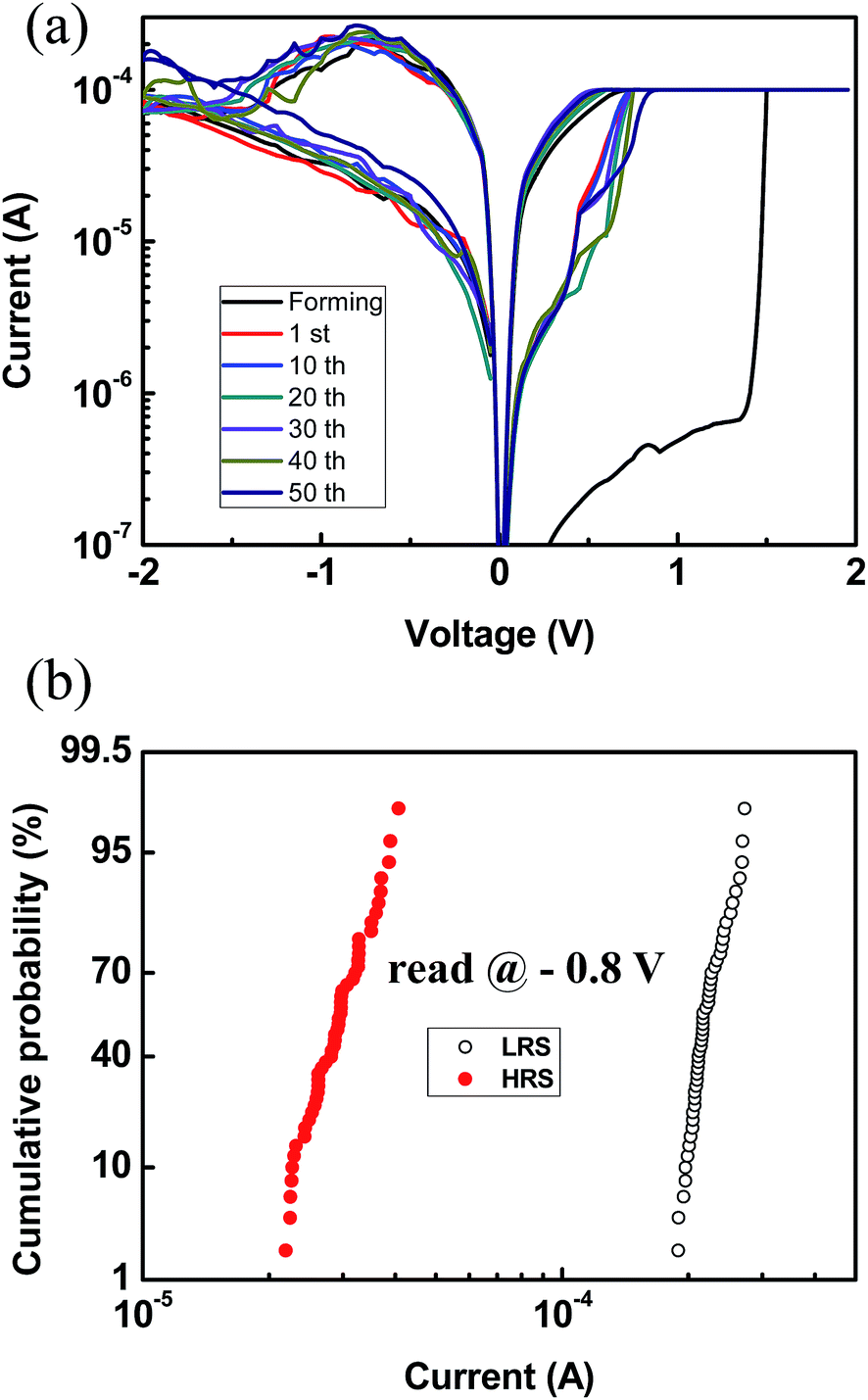 | ||
| Fig. 3 (a) Typical I–V characteristics of Al/AlOx(water)/AlOx(ozone)/Pt and (b) cumulative probability of current values read at −0.8 V. | ||
To determine the mechanisms of conduction and resistive switching of Al/AlOx(water)/AlOx(ozone)/Pt structured RRAM devices, a double logarithmic plot of the I–V curve was drawn in HRS and LRS (Fig. 4). At low bias (<0.4 V) the slopes of the fitted lines in the double logarithmic plot were 1.001 at HRS and 1.014 at LRS; the similarity of the slope to ‘1’ indicates that conduction behavior is ohmic (I ∝ V). In HRS under high bias (>0.4 V), the slope of this line increased to 2.792; this is the Child's law region. As the bias increased past the voltage required for the transition from the ohmic to the space-charge-limited-current (SCLC) regime, injected carriers dominated the conduction behavior.37,38
 | ||
| Fig. 4 Double logarithmic plot of LRS and HRS regions. Linear fitting is shown in the figure. | ||
To investigate the resistive switching mechanism, we measured RRAM devices with Al/AlOx(water)/AlOx(ozone)/Pt structure as above, and compared their characteristics to RRAM devices with Al/AlOx(ozone)/AlOx(water)/Pt structure (i.e., AlOx layers exchanged) while applying positive or negative bias at the top electrode. Al/AlOx(water)/AlOx(ozone)/Pt devices exhibited reliable I–V characteristic, gradual reset behavior, well-behaved bipolar filamentary switching and good uniformity under application of positive bias first (Fig. 5a), but unstable I–V characteristic, abrupt reset behavior and poor uniformity under application of negative bias first (Fig. 5b). In contrast, Al/AlOx(ozone)/AlOx(water)/Pt devices exhibited unstable I–V characteristic, abrupt reset behaviour, and poor uniformity (Fig. 5c) under application of positive bias first, and unstable I–V characteristics, gradual reset behaviour, and poor uniformity (Fig. 5d) under application of negative bias first.
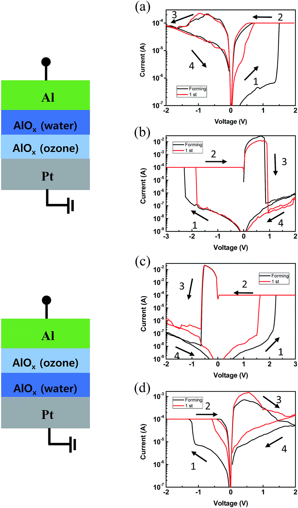 | ||
| Fig. 5 I–V characteristic of Al/AlOx(water)/AlOx(ozone)/Pt with application of (a) positive bias first and (b) negative bias first. I–V characteristic of Al/AlOx(ozone)/AlOx(water)/Pt structure with application of (c) positive bias first and (d) negative bias first. | ||
To determine how the Al top electrode affects the device, we fabricated one with a Pt top electrode instead of an Al top electrode. The I–V characteristics of the Pt/AlOx(water)/AlOx(ozone)/Pt RRAM were similar to those of the Al/AlOx(water)/AlOx(ozone)/Pt devices, such as the gradual reset behavior, set and reset voltage (Fig. 6). However, the Pt/AlOx(water)/AlOx(ozone)/Pt devices were not reliable. Only the devices with Al top electrode showed stable switching behavior.
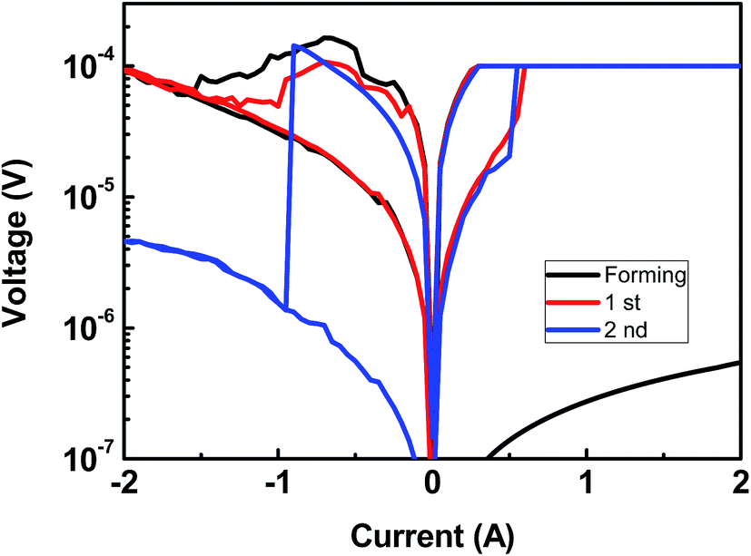 | ||
| Fig. 6 I–V characteristic of Pt/AlOx(water)/AlOx(ozone)/Pt structure. | ||
These results suggest that the switching mechanism of Al/AlOx(water)/AlOx(ozone)/Pt devices is based on the difference in the number of Vos in the two AlOx layers. The AlOx(water) layer has a large number Vos, so conductive filaments remain stable, whereas the AlOx(ozone) layer has few Vos, the conductive filaments partially disassociate. When negative bias is applied, electrons move from the top electrode to the bottom electrode. During this process, the current density increases in interface between AlOx(water) and AlOx(ozone) layer, and conductive filaments partially dissociate in the top part of AlOx(Ozone) layer (Fig. 7). The active Al top electrode which contacts the AlOx layer deposited using water oxidant increases the number of Vos in AlOx(water). It will be very important to know the exact oxygen vacancy concentrations for understanding the exact nature of defects in the resistive switching layer. We synthesized both oxide layers with the same thickness and conditions other than oxidizers (water vs. ozone), but the current–voltage response was very different. Although the exact vacancy concentration is not available it is possible to conclude that the defect concentration is very different according to oxidizers (Fig. S1†).
 | ||
| Fig. 7 Schematics illustration for switching mechanism. | ||
The cycling endurances of Al/AlOx(water)/AlOx(ozone)/Pt devices were measured using consecutive ac voltage pulses to verify the electrical stability under Vset = +2 V and Vreset = −2 V (Fig. 8a). The width of the voltage pulse was 10 ms and the read voltage was −0.3 V. The endurance characteristics varied slightly over time, but both LRS and HRS states retained the memory window without failure for up to 500 cycles. To estimate the non-volatile memory characteristic, data retention tests were performed at RT, 85 °C and 125 °C (Fig. 8b). Both LRS and HRS were read at −0.3 V for 104 s. The current fluctuated, but the memory window was not significantly degraded at any temperature. The stable retention property at elevated temperature (85 °C and 125 °C) indicates good reliability, and shows thermal stability with constant resistance ratio. From retention and endurance characteristics, we conclude that Al/AlOx(water)/AlOx(ozone)/Pt RRAM devices have high uniformity and reliability.
 | ||
| Fig. 8 Reliability of Al/AlOx(water)/AlOx(ozone)/Pt devices. (a) Endurance measurement. (b) Data retention properties measured at RT, 85 °C, and 125 °C. | ||
In the Al/AlOx(water)/AlOx(ozone)/Pt RRAM devices, conductive filaments remain stable in the AlOx(water) layer but the filaments partially dissociated in the AlOx(ozone) layer because the oxide layers have different amounts of Vos. Because filaments partially dissociated in the AlOx(ozone) layer during reset process, Al/AlOx(water)/AlOx(ozone)/Pt RRAM devices exhibit the gradual reset behavior and immune to hard breakdown. The set and reset processes are normally affected by the competition among different filamentary paths at randomly uncertain filament sizes, orientations, and locations, so the process has a random component. However the Al/AlOx(water)/AlOx(ozone)/Pt RRAM devices have restricted set and reset area, resulting in good uniformity and reliability. To ensure the different amounts of Vos between AlOx(water) and AlOx(ozone) layer, top electrode is active Al which contacts the AlOx(water) layer and increases the number of Vos in AlOx(water).
In this experiment, we optimized the bilayer RRAM devices composed of Al/AlOx(water)/AlOx(ozone)/Pt structures; to control the number of Vos, we used two oxidizers. When water was used as the oxidizer the AlOx layer had more Vos than when ozone was used as the oxidizer. Because the oxide layers have different amounts of Vos conductive filaments remain stable in the AlOx(water) layer which has a large number of Vos but the filaments partially dissociated in the AlOx(ozone) layer, which has relatively fewer Vos. Use of an active Al top electrode, can increase the number of Vos in the AlOx(water) layer. The devices exhibit reproducible and reliable RRAM characteristic due to partial dissociation of conductive filaments in the AlOx(ozone) layer.
The main purpose of this work is to show the fabrication of reliable memory devices based on bilayer structure with the same oxide material by changing the oxidizer during deposition. This is very versatile and facile way to fabricate the bilayer structure with different defect concentrations. In addition, this method can simplify the fabrication processes and can effectively reduce the process cost/time.
Conclusions
We used ALD to fabricate RRAM devices composed of Al/AlOx(water)/AlOx(ozone)/Pt structure. After the initial forming process, the devices exhibit reliable and reproducible bipolar resistive switching behavior. Set voltage (Vset) was 0.6 V and reset occurred gradually after −0.8 V. Our devices exhibit stable bipolar switching behavior, switching endurance >500 cycles, and data retention for 104 s at 125 °C. The conduction mechanism was ohmic in LRS and trap-controlled SCLC in HRS. The resistive switching mechanism is related to migration of Vos, which form conductive filaments when an electric field is applied. Joule heating breaks the filaments in AlOx(ozone) layer. Conductive filaments remain stable in the AlOx(water) layer which has a large number of Vos, whereas the filaments partially dissociate in the AlOx(ozone) layer. This work can be a good solution to fabricate reliable RRAM devices since the fabrication process is simple and only single resistive switching material is needed.Acknowledgements
This work was supported by the Future Semiconductor Device Technology Development Program (10045226) funded by the Ministry of Trade, Industry and Energy (MOTIE), and Korea Semiconductor Research Consortium (KSRC). This work was also supported by National Research Foundation of Korea (NRF-2015R1A2A1A15055918). In addition, this work was partially supported by Brain Korea 21 PLUS project (Center for Creative Industrial Materials).Notes and references
- R. Waser and M. Aono, Nat. Mater., 2007, 6, 833–840 CrossRef CAS PubMed.
- A. Sawa, Mater. Today, 2008, 11, 28–36 CrossRef CAS.
- R. Waser, R. Dittmann, G. Staikov and K. Szot, Adv. Mater., 2009, 21, 2632–2663 CrossRef CAS.
- H. Akinaga and H. Shima, Proc. IEEE, 2010, 98, 2237–2251 CrossRef CAS.
- E. Linn, R. Rosezin, C. Kugeler and R. Waser, Nat. Mater., 2010, 9, 403–406 CrossRef CAS PubMed.
- M. Di Ventra and Y. V. Pershin, Mater. Today, 2011, 14, 584–591 CrossRef.
- M. H. Lee and C. S. Hwang, Nanoscale, 2011, 3, 490–502 RSC.
- M. J. Lee, C. B. Lee, D. Lee, S. R. Lee, M. Chang, J. H. Hur, Y. B. Kim, C. J. Kim, D. H. Seo, S. Seo, U. I. Chung, I. K. Yoo and K. Kim, Nat. Mater., 2011, 10, 625–630 CrossRef CAS PubMed.
- J. Park, K. P. Biju, S. Jung, W. Lee, J. Lee, S. Kim, S. Park, J. Shin and H. Hwang, IEEE Electron Device Lett., 2011, 32, 476–478 CrossRef CAS.
- T. Hasegawa, K. Terabe, T. Tsuruoka and M. Aono, Adv. Mater., 2012, 24, 252–267 CrossRef CAS PubMed.
- L. J. Zhang, R. Huang, M. H. Zhu, S. Q. Qin, Y. B. Kuang, D. J. Gao, C. Y. Shi and Y. Y. Wang, IEEE Electron Device Lett., 2010, 31, 966–968 CrossRef CAS.
- Z. Fang, H. Y. Yu, X. Li, N. Singh, G. Q. Lo and D. L. Kwong, IEEE Electron Device Lett., 2011, 32, 566–568 CrossRef CAS.
- J. W. Seo, S. J. Baik, S. J. Kang, Y. H. Hong, J. H. Yang and K. S. Lim, Appl. Phys. Lett., 2011, 98, 233505 CrossRef.
- Y. Wu, S. M. Yu, B. Lee and P. Wong, J. Appl. Phys., 2011, 110, 094104 CrossRef.
- S. Yu, H. Y. Chen, B. Gao, J. Kang and H. S. Wong, ACS Nano, 2013, 7, 2320–2325 CrossRef CAS PubMed.
- J.-M. Song and J.-S. Lee, Sci. Rep., 2016, 6, 18967 CrossRef CAS PubMed.
- Y. Wu, S. M. Yu, B. Lee and P. Wong, J. Appl. Phys., 2011, 110 Search PubMed.
- D. S. Jeong, R. Thomas, R. S. Katiyar, J. F. Scott, H. Kohlstedt, A. Petraru and C. S. Hwang, Rep. Prog. Phys., 2012, 75, 076502 CrossRef PubMed.
- S. Lee, W. G. Kim, S. W. Rhee and K. Yong, J. Electrochem. Soc., 2008, 155, H92–H96 CrossRef CAS.
- S. Takata, R. Tanaka, A. Hachiya and Y. Matsumoto, J. Appl. Phys., 2011, 110, 103513 CrossRef.
- S. S. Lee, E. S. Lee, S. H. Kim, B. K. Lee, S. J. Jeong, J. H. Hwang, C. G. Kim, T. M. Chung and K. S. An, Bull. Korean Chem. Soc., 2012, 33, 2207–2212 CrossRef CAS.
- W. Kim, S. I. Park, Z. P. Zhang and S. Wong, IEEE Trans. Electron Devices, 2014, 61, 2158–2163 CrossRef CAS.
- L. Assaud, M. Hanbuecken and L. Santinacci, in Atomic Layer Deposition Applications 8, ed. J. W. Elam, A. Londergan, O. VanDerStraten, F. Roozeboom, S. DeGendt, S. F. Bent and A. Delabie, 2012, pp. 151–157 Search PubMed.
- J. Hu and H. S. P. Wong, J. Appl. Phys., 2012, 111, 044105 CrossRef.
- L. G. Wang, X. Qian, Y. Q. Cao, Z. Y. Cao, G. Y. Fang, A. D. Li and D. Wu, Nanoscale Res. Lett., 2015, 10, 135 CrossRef PubMed.
- S. M. Sadaf, X. Liu, M. Son, S. Park, S. H. Choudhury, E. Cha, M. Siddik, J. Shin and H. Hwang, Phys. Status Solidi A, 2012, 209, 1179–1183 CrossRef CAS.
- A. Prakash, S. Maikap, C. S. Lai, T. C. Tien, W. S. Chen, H. Y. Lee, F. T. Chen, M. J. Kao and M. J. Tsai, Solid-State Electron., 2012, 77, 35–40 CrossRef CAS.
- R. C. Fang, Q. Q. Sun, P. Zhou, W. Yang, P. F. Wang and D. W. Zhang, Nanoscale Res. Lett., 2013, 8, 92 CrossRef PubMed.
- Y. Bai, H. Q. Wu, Y. Zhang, M. H. Wu, J. Y. Zhang, N. Deng, H. Qian and Z. P. Yu, Appl. Phys. Lett., 2013, 102, 173503 CrossRef.
- Y. Zhang, H. Wu, Y. Bai, A. Chen, Z. Yu, J. Zhang and H. Qian, Appl. Phys. Lett., 2013, 102, 233502 CrossRef.
- H. Zhang, N. Aslam, M. Reiners, R. Waser and S. Hoffmann-Eifert, Chem. Vap. Deposition, 2014, 20, 282–290 CrossRef CAS.
- C. W. Hsu, Y. F. Wang, C. C. Wan, I. T. Wang, C. T. Chou, W. L. Lai, Y. J. Lee and T. H. Hou, Nanotechnology, 2014, 25, 165202 CrossRef PubMed.
- C. Y. Huang, C. Y. Huang, T. L. Tsai, C. A. Lin and T. Y. Tseng, Appl. Phys. Lett., 2014, 104, 062901 CrossRef.
- C.-T. Chou, B. Hudec, C.-W. Hsu, W.-L. Lai, C.-C. Chang and T.-H. Hou, Microelectron. Reliab., 2015, 55, 2220–2223 CrossRef CAS.
- H. J. Lee, M. H. Park, Y. S. Min, G. Clavel, N. Pinna and C. S. Hwang, J. Phys. Chem. C, 2010, 114, 12736–12741 CAS.
- O. B. F. Campabadal, M. Zabala, M. C. Acero and J. M. Rafí, Proceedings of the 8th Spanish Conference on Electron Devices, 2011 Search PubMed.
- L. E. Yu, S. Kim, M. K. Ryu, S. Y. Choi and Y. K. Choi, IEEE Electron Device Lett., 2008, 29, 331–333 CrossRef CAS.
- E. Lim and R. Ismail, Electronics, 2015, 4, 586–613 CrossRef.
Footnote |
| † Electronic supplementary information (ESI) available. See DOI: 10.1039/c6ra00798h |
| This journal is © The Royal Society of Chemistry 2016 |