
High-performance dye-sensitized solar cell using dimensionally controlled titania synthesized at sub-zero temperatures†
Kiran P. Shejale,
Devika Laishram and
Rakesh K. Sharma*
Department of Chemistry, Indian Institute of Technology Jodhpur, Jodhpur, 342011, India. E-mail: rks@iitj.ac.in
First published on 24th February 2016
Abstract
The subject of the current study is a concoct of anatase and rutile mixed phase titania synthesized at −40 °C and −10 °C. At these sub-zero temperatures, highly crystalline, phase-oriented nanostructured titania were formed. At −40 °C, nanocrystals of TiO2 consist of the anatase phase while nanorods dominated by the rutile phase form at −10 °C. These samples are remarkable photoanode materials with excellent photon scattering ability in dye-sensitized solar cells (DSSCs). On performance optimization of DSSCs, a composition of 0.5 wt% TiO2 (prepared at −40 °C) and P25 improved the photon harvesting by providing a large number of sites for interaction, resulting in a high photocurrent of 18.46 mA cm−2 and 8.6% photoconversion efficiency.
Introduction
Nanocrystalline TiO2 is one of the most studied low-cost, non-toxic and stable wideband semiconducting materials. It exhibits a broad range of unique optical, electrical and photocatalytic properties, which are mainly governed by its morphology and phase.1–5 This allows for a wide variety of application in the areas of gas sensors, paints, catalysis, optics, dielectric materials, pigments, solar cells and inorganic membranes.6–8 Among these, the use of TiO2 in DSSCs attracted considerable attention when Gratzel and coworkers reported a DSSC with 7% photoconversion efficiency, followed by numerous studies to understand the working principle behind the electrochemical solar cell.9–12 With advancements made in DSSC, TiO2 became one of the most investigated and sought after material for photoanode applications. Out of many factors, structural and physical properties of TiO2 play most crucial role in DSSC performance,13,14 governed by crystal size, morphology, composition, porosity and surface area.15 Tuning and modification in these properties at nanoscale titania expected to be a promising strategy to improve photo current density in DSSC applications. Significant efforts have been made towards structural optimization of TiO2 photoanode such as particle size, hierarchical, 1D–3D, hollow structures, aggregates and micro-sized spheres,16,17 and it was observed that crystalline size, morphology and phase composition have profound effect on the light scattering property to harvest more photon, dye loading, recombination properties and electron transport in DSSCs, they have received extensive attention, and shown improved performance of the DSSCs.18,19Crystalline TiO2 is found as three polymorphs in nature – anatase, rutile and brookite phase.20 Synthetically, anatase crystalline phase is prepared at mild thermal treatment below 400 °C, whereas rutile forms at a higher temperature.21 Various strategies have been employed such as annealing, doping and physical mixing to modify structural and physical properties of titania.22–24 Historically titania is prepared in highly acidic/basic condition or at high temperature that make these processes cumbersome at large scale, accompanied with undesirable phase transformations that limits their applications.25–27 These synthetic limitations are noteworthy to obtain functional nano-TiO2. A simple but perspicacious change in synthetic temperature could lead to thermodynamically controlled growth of nanoparticle of TiO2, particularly at low temperature. Most often low temperature studies are carried out in room temperature with a few exceptions going low as 4 °C, where TiO2 hydrosols were obtained by refluxing titanium ethoxide [entry 30 from Table A2, ESI†], lately, the first investigation on synthesis of nano-titania at sub-zero temperature has been reported by Sharma and coworkers.28 The detailed low temperature crystallization of TiO2 with their crystalline phase are mentioned in Table S2, ESI.†
In our recent work, we have reported a simple one step, sub-zero temperature method to synthesize well crystallized anatase and rutile nanoparticles with controlled size and shape.28 Synergetic effect between the phase composition and variation in shape and size of TiO2 nanoparticles was demonstrated. In this study, two temperatures were selected based on two distinct reasons, first, the TiO2 synthesized at −40 °C and −10 °C clearly point towards drastic changes in texture and phase combination. Second, the band gap of both the samples were found to have significant difference and expected to have better light harvesting in DSSC (Fig. S1, ESI†). The factors affecting the morphology of the synthesized TiO2 nanoparticles at low temperature have been explored and the collaborative role of the mixed phase and different size with shape have been analyzed using them as photoanode material in DSSC.
Experimental section
Materials
Titanium(IV) isopropoxide (TTIP) and titanium tetrachloride (TiCl4) (>99%) were purchased from Spectrochem. Hydrochloric acid (>37%) and nitric acid (68–70%) were acquired from Fisher Scientific. Ethanol (absolute > 99.8%), terpineol (>98%), acetic acid (glacial > 96%) and ethyl cellulose (44–51%) were obtained from Changshu Yangyuan, Alfa Aesar, Qualigens and Himedia respectively. P25 commercial TiO2 nanoparticles was purchased from Degussa. Fluorine doped tin oxide (FTO) glass, electrolyte solution Iodolyte Z-50, Meltonix (Surlyn), Platisol-T and N719 Ruthenizer 535-bis TBA were purchased from Solaronix. Silver conductive paste (Pelco-colloidal Silver liquid) was acquired from Ted Pella, Inc.TiO2 synthesis
TiO2 nanoparticles of different morphologies and size were prepared using reactor chamber (Radley). Overhead stirrer mounted on the reactor (Heldoph RZR 2102 control) was used to maintain the stirring speed at 350 rpm. The thermoregulator (Huber unistat 705) was connected to the reactor ready chamber to obtain the desired reaction temperature. By controlling the reaction temperatures at −40 °C and −10 °C, mixture of 80 mL TTIP, 1000 mL ethanol and 400 mL distilled water were stirred for 24 hours in the reactor. Nitric acid was used to control reaction pH up to 1.5. The resultant solution was dried and annealed at 100 °C for 12 hours. To optimize results, three samples S1, S2 and S3 were prepared consisting of 0%, 40% and 100% of TiO2 prepared at −40 °C and the remaining amount was made up with TiO2 prepared at −10 °C that is 100%, 60% and 0% respectively.Preparation of electrodes and device fabrication
![[thin space (1/6-em)]](https://www.rsc.org/images/entities/char_2009.gif) :6 (weight ratio) using which screen printing paste was prepared with the addition of ethanol, terpineol, acetic acid and ethyl cellulose. The printing process was repeated several times to get the desired film thickness. Firstly sintered at 500 °C for 15 min and after post treating with 40 mM TiCl4 aqueous solution for 30 min at 70 °C, the photoanodes were sintered again at 520 °C for 30 min. The sample photoanodes were then immersed into 0.5 mM N719 dye for 20 hours.
:6 (weight ratio) using which screen printing paste was prepared with the addition of ethanol, terpineol, acetic acid and ethyl cellulose. The printing process was repeated several times to get the desired film thickness. Firstly sintered at 500 °C for 15 min and after post treating with 40 mM TiCl4 aqueous solution for 30 min at 70 °C, the photoanodes were sintered again at 520 °C for 30 min. The sample photoanodes were then immersed into 0.5 mM N719 dye for 20 hours.Characterization
Powder X-ray diffraction (XRD) analysis of the prepared samples were performed using Bruker D8 Advance diffractometer equipped with Cu Kα radiation having 1.54 Å wavelength Bruker AXS (11/03-2370) as source and Bruker (C79298-A3178-A15) as detector. Raman spectra of both samples were performed at room temperature using Renishaw instruments with an emission wavelength of 514 nm. Scanning electron microscope (SEM) micrograph of the TiO2 film as photoanode was analysed by the Zeiss EVO 18 Special Edition microscope. Transmission electron microscope (TEM) images of the samples were obtained by a FEI Tecnai-G2 T20 operated at 200 kV. The photoanode film surfaces was examined by Park System XE-70 atomic force microscope (AFM). The diffuse reflectance spectra of both samples and all the photoanodes were carried out by UV-visible spectrophotometer (Varian Cary 4000) using diffuse reflectance spectroscopy accessory over a wavelength range of 200–800 nm. And same instrument was used to calculate the amount of eluted N719 dye quantity adsorbed on all the photoanodes. The dye loaded photoanodes were dipped in 6 mL of 10 mM NaOH in distilled water for 30 min. The current density–voltage and electrochemical impedance spectroscopy (EIS) measurements were recorded by an electrochemical work station CHI660E-CH Instruments Inc. under one sun irradiation by SS50AAA solar simulator model from PET Photo Emission Tech., Inc. Electrochemical impedance study of the cells were also recorded at 1 Hz to 0.1 MHz.Results and discussion
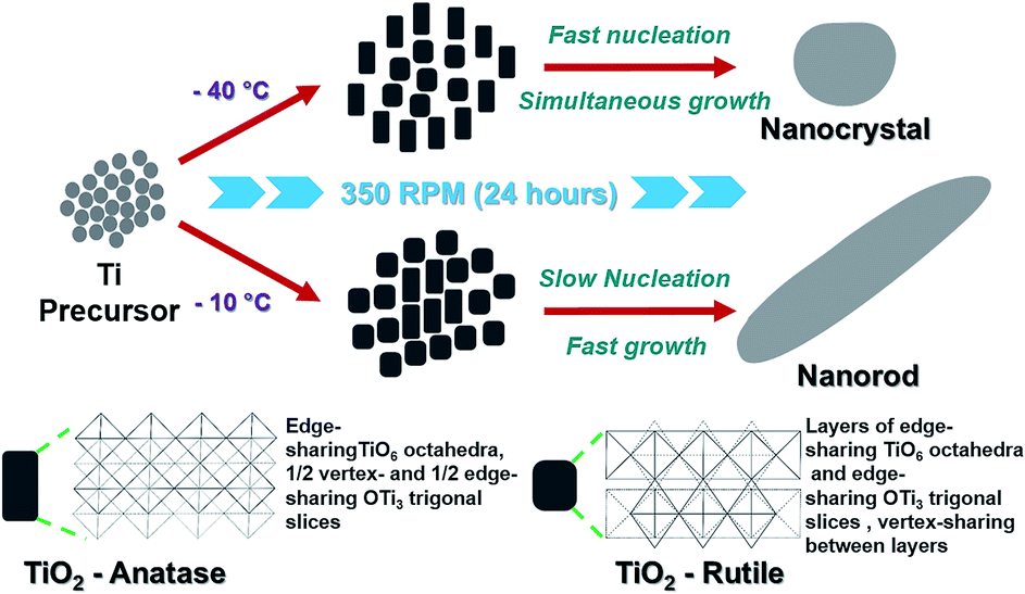
A pervasive work was done to synthesize TiO2 with controlled size and morphology as demonstrated in Fig. 1a. Briefly, the reaction was carried out using titanium isopropoxide precursor in ethanol and deionized water at controlled temperatures of −40 °C and −10 °C as illustrated by the schematic in Fig. 1a. The morphologies of TiO2 prepared at −40 °C and −10 °C were characterized by XRD as shown in Fig. 1b and c. Interestingly, the peaks in Fig. 1b are broader as compared to Fig. 1c which indicates the formation of small size particle. The diffraction peaks at 25.3 and 27.5 are assigned to (101) and (110) planes and are matching with JCPDS reference spectra of TiO2 anatase 21-1271 (tetragonal) and TiO2 rutile 21-1276 (tetragonal) as shown in Fig. 1b and c respectively. The XRD patterns of TiO2 prepared at −10 °C and −40 °C indicate change in the size and phase percentile in the product. | ||
| Fig. 1 (a) Schematic demonstration of TiO2 synthesis process. (b) and (c) XRD spectra of synthesized TiO2 at −40 °C and −10 °C respectively along with bar line graphs shows the XRD spectra of rutile and anatase TiO2 JCPDS data. (d) and (e) Raman spectra for TiO2 synthesized at −40 °C and −10 °C respectively with a 532 nm wavelength diode laser respectively. | ||
TiO2 prepared at −40 °C display Raman active peaks having highest intensity peak (eg) at 150 cm−1 and other peaks (a1g, eg and 2b1g) suggesting towards high percentage of anatase phase as shown in Fig. 1d. However in Fig. 1e, the TiO2 sample prepared at −10 °C confirms the high percentage of rutile phase showing (eg and a1g) Raman active peaks at 443 cm−1 and 608 cm−1 respectively. The peak at 254 cm−1 is due to multiple phonon scattering process known as compound vibrational peak.29–31 The strain present on the grain boundaries, oxygen vacancies, temperature, particle size etc. are known to directly influence the Raman peaks.32 A small shift in band positions might be due to phonon confinement, lattice strain, crystalline size and oxygen defects.33 The crystallographic phases of both TiO2 analyzed by Raman spectroscopy are in accordance with the above XRD findings and revealed the presence of both anatase and rutile crystallographic phases in both the samples. The detailed information of anatase and rutile crystallographic Raman phases is provided in Note S1, ESI.† Using diffraction peak intensities of rutile (110) and anatase (101), the weight percentage of rutile was estimated to be 73% and 42% for samples prepared at −10 °C and −40 °C respectively (see Note S2, ESI†). Broad diffraction peaks of both samples were indicating towards small size particles accompanied with defects around their grain boundaries. These defects generate strain in the grain boundaries which have a direct impact on the growth of the nanoparticles.34,35 The lattice strain present at the grain boundary along with particle size (D) are calculated for the samples using diffraction peaks of linearly fitted graphs with βcosθ/λ as X-axis and sinθ/λ as Y-axis as shown in Fig. S2, Note S3, ESI† and Table 1. High lattice strain, 0.0367, at −40 °C is a result of more number of atoms accompanied with defects in the grain boundary. The change in phase combination is determined by interface nucleation and these two factors produces stress on the grain boundaries.36 At −10 °C, lattice strain decreasing to 0.0323 indicate towards reduced grain boundary defects and accelerates the growth thereby forming bigger size particle. The reaction temperature increases reduced defects at grain boundary results in the formation of rutile phase in the sample.
TEM analysis was carried out to confirm the size and morphology of the TiO2 prepared at −40 °C and −10 °C (see Fig. 2a and b and Table 1). TiO2 synthesized at −40 °C was found to be oval in shape with 3.78 nm as average particle size whereas at −10 °C nanoparticle was in rod shape exhibit average width as 4.59 nm with 16.54 nm in length. Fig. 2c and d are the HRTEM image of −40 °C and −10 °C showing inter planar distance with anatase and rutile as dominating phase, respectively. Respective dominating phases were also observed in SAED pattern of −40 °C and −10 °C shown in Fig. 2e and f respectively. Small crystal nuclei of both TiO2 structure will form depending on the surrounding temperature.37–40 At −40 °C and −10 °C, difference in the particles size and shape originates from crystal structure consisting different arrangement in TiO6 octahedral units; anatase (zigzag packing) and rutile (linear packing) shown in Fig. 3.41 In anatase, cis-coordination and in rutile trans-coordination sites of octahedra are used for crystal growth. Some have reported that the phase and shape of the TiO2 nanoparticles formed from crystal growth are governed by anions and solvents.42–44 As temperature increases, the thermal conditions are able to form closest linear packing of the TiO6 octahedral units.45 In our case as shown schematically in Fig. 3, at transition initiation temperature of −10 °C, mostly rutile crystals are formed indicating that nucleation is relatively slower than the growth rate thus forming rod shaped nanoparticles with linearly packed TiO6 octahedral units which exhibits less strain (0.0323, see ESI Fig. S2†) on the particles. Where at −40 °C, growth occurs simultaneously with fast nucleation leading to anatase phase with zigzag packed crystal structure as also reflected from high strain (0.0367, see ESI Fig. S2†) on the particle surface. This probably explains the formation of nanorods and nanocrystals with phase transition from anatase to rutile at sub-zero synthesis temperatures.
 | ||
| Fig. 2 (a) and (b) TEM images, (c) and (d) HRTEM images with marked inter planar distance and (e) and (f) are SAED pattern of −40 °C and −10 °C respectively. Dotted lines in (e) and (f) are guide to eye. | ||
 | ||
| Fig. 3 Schematic illustration of TiO2 synthesis process. | ||
The optical band gap of both TiO2 samples mentioned in Table 1 were estimated by Tauc plot and Kubelka–Munk expression using % reflectance values.46,47 Fig. 4 with inset demonstrates % R and band gap analysis respectively. Reaction temperature increases from −40 °C to −10 °C, increment of the rutile% were reported in samples allow narrowing band gap from 3.02 to 2.97 eV respectively. These change was also induced by the nucleation, growth rate and stress present on the grain boundaries which were produced by defects and particle size.48 If these samples will be used as photoanodes in DSSC, wider band gap will reduce recombination in the DSSC allowing more electrons to jump from the excited state of the dye to the conduction band of TiO2.
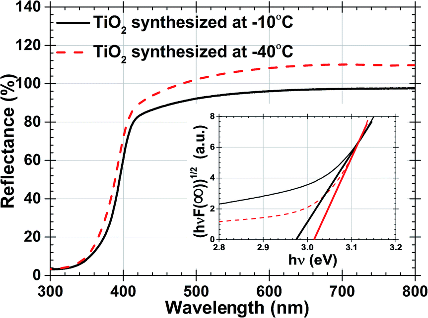 | ||
| Fig. 4 Percentage reflectance data of TiO2 synthesized at −10 °C and −40 °C. And inset shows hν and (hνF(R∞))(1/2) plot. | ||
To optimize DSSC performance, three samples S1, S2 and S3 were prepared with 0, 16 and 40 of wt% of TiO2 prepared at −40 °C in respective samples, the detailed composition is illustrated in the form of a bargraph in Fig. 5a. The film surface morphology and the average root mean square roughness (Rrms) of S1, S2 and S3 samples are shown in the Fig. S3, ESI† and are listed in Table 2. The films show columnar microstructure accompanied by spherical grain structure suggesting that it constitutes nanorods with oval shaped nanoparticles.
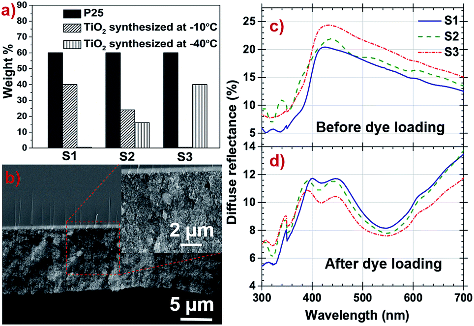 | ||
| Fig. 5 (a) Bargraph shows the composition of S1, S2 and S3. (b) Cross sectional image of film S1 and inset SEM image show uniformly oriented nanoparticles with high porosity. (c) and (d) Diffuse reflectance spectra of S1, S2 and S3 photoanodes before and after dye loading respectively. | ||
| Sample | wt% of TiO2 prepared at −40 °C in sample | Rrms (μm) | Dye loading amount (×10−9 mol cm−2) |
|---|---|---|---|
| a These values refer to the percentage of the TiO2 prepared at −40 °C in sample and film surface root mean square roughness, Rrms. | |||
| S1 | 0 | 0.069 | 3.6066 |
| S2 | 16 | 0.101 | 3.9421 |
| S3 | 40 | 0.130 | 4.2392 |
The cross sectional film morphology was obtained by SEM (Fig. 5b), the average thickness of the film was found to be 14.5 μm. The film thickness is optimized in the range of 10–18 μm range and its uniformity are the main parameters which control the reproducibility of the DSSC performance. Above this range, thickness produces resistance to electrons travelling through TiO2 and also decreases the number of photons encountered by dye molecules. Below the optimized range number of anchoring site for dye molecules reduces. The inset of Fig. 5b shows uniformly distributed samples along the photoanode films with a highly porous structure.
Light scattering property of photoanode films is one of the important attributers in light harvesting efficiency of the DSSC.49,50 The diffused reflectance of S3 film is higher as compared to the other photoanode films before dye loading as shown in Fig. 5c. High percentage of anatase having different sized nanoparticles with higher surface roughness attributes to increased light scattering in S3 film and will harvest more light during photo conversion. After dye loading, diffused reflectance of all photoanode films were decreased significantly due to light absorption by the dye and are shown in Fig. 5d. The dyed S3 photoanode film is reported to have more absorption with lower diffused reflectance in the 350–700 nm region compared to other samples.
The amount of dye loading at photoanodes directly have profound effect on the photocurrent density are summarized in Table 2, Fig. S4 and Note S4, ESI.† The measured dye loading behaviour matches with the trend of the UV-vis reflectance data. The specific surface area is directly correlated to different size particle distribution along the photoanode films, also the roughness of the films have to be considered as a significant factor which directly influence the amount of dye loading. This provides more number of sites to anchor dye molecules and shows S3 photoanode's dye loading capacity is higher compared to other samples (4.2392 × 10⁻⁹ mol cm−2).
The schematic diagram of DSSC is presented in Fig. 6a and a photograph of one of the fabricated DSSC is shown in the inset of same. The current density–voltage curve and parameters of all DSSCs are reported in Fig. 6b and Table 3 respectively. It has been observed that pristine P25, TiO2 synthesized at −40 °C or at −10 °C were able to achieve 11.4 mA cm−2 of photocurrent while S1, S2 and S3 combinations show remarkably higher photocurrent (see ESI Table A1†). The S3 photoanode DSSC have high anatase percentage with oval shaped nanoparticles exhibiting high specific surface area with more sites to anchor more dye which eventually combines yielding enhanced photo-conversion efficiency and reported high efficiency of 8.6% compared to the other samples. Improving DSSC performance depends on the enhancement of the photocurrent Jsc which can be credited to the well-developed light scattering structure of the photoanode which increases the light harvesting, as the open circuit voltage Voc and fill factor (FF) have little difference among the cells. Reduced photocurrent in S2 and S3 can be explained by the less dye loading due to higher percentage of nanorods composition, low roughness and decreased sites to attach dye. Also, band gap of the TiO2 prepared at −40 °C is wider than −10 °C, which exhibits faster electron transport at the interfaces.51 It appears clearly from the above findings that efficiency is a function of percentage of the TiO2 synthesized at −40 °C in photoanodes, although particle size and shape also show their direct impact on the cell efficiency.
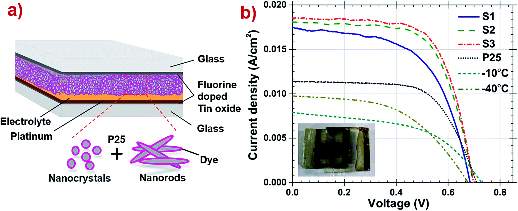 | ||
| Fig. 6 (a) Schematic representation of fabricated DSSC. (b) Current density–voltage curves of the DSSC consisting −40 °C, −10 °C, P25, S1, S2 and S3 samples as photoanodes under one sun illumination. | ||
| Sample | wt% of anatase | Jsc (mA cm−2) | Voc (V) | FF | η (%) |
|---|---|---|---|---|---|
| a Short circuit current density, Jsc, open circuit voltage, Voc, fill factor, FF and photoconversion efficiency, η are the parameters of DSSC examined at AM 1.5G 1000 W m−2 by keeping 0.09 cm2 as the working area for all the solar cells. | |||||
| −40 °C | 58 | 9.69 ± 0.9 | 0.68 ± 0.01 | 50.8 ± 0.9 | 3.3 ± 0.02 |
| −10 °C | 27 | 7.86 ± 0.02 | 0.73 ± 0.01 | 50.79 ± 0.2 | 2.9 ± 0.05 |
| P25 | 80 | 11.4 ± 0.01 | 0.71 ± 0.01 | 64 ± 0.01 | 5.2 ± 0.08 |
| S1 | 59 | 17.44 ± 1.4 | 0.68 ± 0.01 | 57.67 ± 0.33 | 6.9 ± 0.5 |
| S2 | 64 | 18.07 ± 0.7 | 0.7 ± 0.02 | 65.54 ± 1.54 | 8.2 ± 0.8 |
| S3 | 71 | 18.46 ± 0.4 | 0.7 ± 0.01 | 66.46 ± 1.46 | 8.6 ± 0.3 |
EIS has been widely used to analyse various parameters attributed to electrons transport in the TiO2 interface and recombination between electron at LUMO level of dye and the redox electrolyte are listed in the Table 4. Inset of Fig. 7a shows the equivalent circuit of all fabricated DSSCs. Under illumination, sheet resistance is observed as almost same for all DSSCs and as identical Pt counter electrodes were used during the fabrication, there is no significant change in the value of R1. In such condition charge transport resistance R2 decreased in S3 resulting in fast electron transport at electrolyte–dye–photoanode junction in the S3 DSSC shown in Fig. 7a. In dark condition EIS shown in Fig. 7b, no electron jumped from LUMO level of dye to TiO2 and it implies transport of electrons to the electrolyte specimen. So R2 transport resistance attributes recombination rate at these junction.52,53 The sheet resistance (Rs) is the combine value of resistance of the FTO glass, contact resistance of the DSSC and resistance created due to external circuits. The charge transfer between Pt counter electrode and electrolyte is demonstrated by first semicircle (R1). The electron transfer at electrolyte–dye–photoanode interface serves as charge transport and recombination represented by the intermediate semicircle (R2). Diffusion of the iodide species in electrolyte is shown by the third semicircle.54
| DSSC | Under illumination | In dark | ||||
|---|---|---|---|---|---|---|
| Rs/Ω | R1/Ω | R2/Ω | Rs/Ω | R1/Ω | R2/Ω | |
| a Sheet resistance and series resistance are obtained under illumination at AM 1.5G 1000 W m−2 and in dark. The derived parameters are corresponds to high performed cells in Table 3. | ||||||
| S1 | 14.97 | 17.47 | 4.817 | 15.12 | 30.53 | 12.53 |
| S2 | 14.82 | 19.11 | 4.63 | 15.45 | 26.73 | 3.757 |
| S3 | 15.14 | 15.66 | 3.124 | 12.72 | 35.37 | 4.575 |
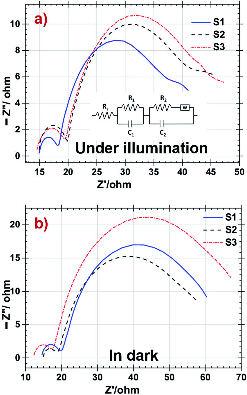 | ||
| Fig. 7 Nyquist plot of DSSC with S1, S2 and S3 samples as photoanodes (a) under illumination and (b) in dark respectively. | ||
Conclusions
This work states the detailed and complete analysis of TiO2 synthesized by one step sub-zero temperature method with well crystallized anatase and rutile nanoparticles. The reaction temperature of synthesis process exhibits variation in phase composition which implies morphological changes such as size and shape of nanoparticles. This change is mainly caused by phase combination, lattice strain, defects present on the grain boundaries and nucleation-growth rate of particles. These materials were used as photoanode for DSSC. Remarkably, enhancement in both photocurrent density and photo-conversion efficiency, 18.46 mA cm−2 and 8.6% respectively were reported for the S3 DSSC. Enhancement arises from high percentage of anatase phase (0.5%), optimized film thickness (14.5 μm), increased charge transport along with decrease in recombination rate at electrolyte–dye–photoanode (3.124/Ω), higher Rrms (0.130 μm) with different size and shape nanoparticles harvest more light. The present work provides a simple, controlled one step process to synthesize TiO2 and its application in DSSC with high performance open window towards more applications like batteries, photocatalysis and biosensors etc.Acknowledgements
The authors are grateful to Department of Science and Technology, Govt. of India and Indo-Portuguese program of cooperation in science and technology, 2014–2016 (Grant No. SR/FT/CS-144/2011 and INT/Portugal/P02/2013) in terms of financial support. The authors would like to thank Dr Ritu Gupta for helping out with the correction. We would also like to acknowledge the Material Research Centre, MNIT Jaipur, India for providing TEM Characterization facility.References
- T. A. Kandiel, A. Feldhoff, L. Robben, R. Dillert and D. W. Bahnemann, Chem. Mater., 2010, 22, 2050 CrossRef CAS
.
- B. Liu and E. S. J. Aydil, J. Am. Chem. Soc., 2009, 131, 3985 CrossRef CAS PubMed
- H. Zhang, G. Chen and D. W. Bahnemann, J. Mater. Chem., 2009, 19, 5089 RSC
- X. M. Song, J. M. Wu, M. Z. Tang, B. Qi and M. Yan, J. Phys. Chem. C, 2008, 112, 19484 CAS
- K. Ding, Z. Miao, B. Hu, G. An, Z. Sun, B. Han and Z. Liu, Langmuir, 2010, 26, 10294 CrossRef CAS PubMed
- W. Li, C. Ni, H. Lin, C. P. Huang and S. I. Shah, J. Appl. Phys., 2004, 96, 6663 CrossRef CAS
- X. Chen and S. S. Mao, Chem. Rev., 2007, 107, 2891 CrossRef CAS PubMed
- G. Madras and B. J. McCoy, Cryst. Growth Des., 2007, 7, 250 CAS
- H. Lin, X. Li, Y. Liu and J. Li, Mater. Sci. Eng., B, 2009, 161, 2 CrossRef CAS
- M. Gratzel, Nature, 2001, 414, 338 CrossRef CAS PubMed
- B. O'Regan and M. Gratzel, Nature, 1991, 353, 737 CrossRef
- P. V. V. Jayaweera, A. G. U. Perera and K. Tennakone, Inorg. Chim. Acta, 2008, 361, 707 CrossRef CAS
- A. Hagfeldt, G. Boschloo, L. C. Sun, L. Kloo and H. Pettersson, Chem. Rev., 2010, 110, 6595 CrossRef CAS PubMed
- Y. Xiong, D. He, Y. Jin, P. J. Cameron and K. J. Edler, J. Phys. Chem. C, 2015, 119, 22552 CAS
- Z. Q Li, Y. Ding, L. E. Mo, L. H. Hu, J. H. Wu and S. Y. Dai, Appl. Mater. Interfaces, 2015, 7, 22277 CrossRef PubMed
- T. G. Deepak, G. S. Anjusree, S. Thomas, T. A. Arun, S. V. Nair and A. S. Nair, RSC Adv., 2014, 4, 17615 RSC
- H.-J. Koo, J. Park, B. Yoo, K. Yoo, K. Kim and N.-G. Park, Inorg. Chim. Acta, 2008, 361, 677 CrossRef CAS
- Z.-S. Wang, H. Kawauchi, T. Kashima and H. Arakawa, Coord. Chem. Rev., 2004, 248, 1381 CrossRef CAS
- I. G. Yu, Y. J. Kim, H. J. Kim, C. Lee and W. I. Lee, J. Mater. Chem., 2010, 21, 532 RSC
- G. K. Mor, K. Shankar, M. Paulose, O. K. Varghese and C. A. Grimes, Nano Lett., 2006, 6, 215 CrossRef CAS PubMed
- Y. W. Jun, M. F. Casula, J. H. Sim, S. Y. Kim, J. Cheon and A. P. Alivisatos, J. Am. Chem. Soc., 2003, 125, 15981 CrossRef CAS PubMed
- Y. Kakuma, A. Y. Nosaka and Y. Nosaka, Phys. Chem. Chem. Phys., 2015, 17, 18691 RSC
- Y. Du, Q. Feng, C. Chen, Y. Tanaka and X. Yang, ACS Appl. Mater. Interfaces, 2014, 6, 16007 CAS
- J. H. Shim and J. Cho, J. Am. Ceram. Soc., 2016, 99, 431 CrossRef CAS
- H. Zhang and J. F. Banfield, J. Phys. Chem. B, 2000, 104, 3481 CrossRef CAS
- M. R. Ranade, A. Navrotsky, H. Z. Zhang, J. F. Banfield, S. H. Elder, A. Zaban, P. H. Borse, S. K. Kulkarni, G. S. Doran and H. J. Whitfield, Proc. Natl. Acad. Sci. U. S. A., 2002, 99, 6476 CrossRef CAS PubMed
- H. Zhang and J. F. Banfield, J. Mater. Chem., 1998, 8, 2073 RSC
- K. P. Shejale, D. Laishram, M. S. Roy, M. Kumar and R. K. Sharma, Mater. Des., 2016, 92, 535 CrossRef
- W. F. Zhang, Y. L. He, M. S Zhang, Z. Yin and Q. Chen, J. Phys. D: Appl. Phys., 2000, 33, 912 CrossRef CAS
- J. Zhang, M. Li, Z. Feng, J. Chen and C. Li, J. Phys. Chem. B, 2006, 110, 927 CrossRef CAS PubMed
- S. M. Mali, C. A. Betty, P. N. Bhosale and P. S. Patil, CrystEngComm, 2011, 13, 6349 RSC
- D. Wang, J. Zhao, B. Chen and C. Zhu, J. Phys.: Condens. Matter, 2008, 20, 085212 CrossRef
- M. Ocana, V. Fornes, J. V. Ramos and C. J. Serna, J. Solid State Chem., 1988, 75, 364 CrossRef CAS
- B. Choudhury and A. Choudhury, Mater. Chem. Phys., 2012, 131, 666 CrossRef CAS
- W. Qin and J. A. Szpunar, Philos. Mag. Lett., 2005, 85, 649 CrossRef CAS
- D. A. H. Hanaor and C. C. Sorrell, J. Mater. Sci., 2011, 46, 855 CrossRef CAS
- Y. Yu, Q. Zhang, J. Xie and J. Y. Lee, Nat. Commun., 2013, 4, 1454 CrossRef PubMed
- X. Peng, J. Wickham and A. P. Alivisatos, J. Am. Chem. Soc., 1998, 120, 5343 CrossRef CAS
- Y. W. Jun, J. S. Choi and J. Cheon, Angew. Chem., Int. Ed., 2006, 45, 3414 CrossRef CAS PubMed
- L. Manna, E. C. Scher and A. P. Alivisatos, J. Am. Chem. Soc., 2000, 122, 12700 CrossRef CAS
- N. Satoh, T. Nakashima and K. Yamamoto, Sci. Rep., 2013, 3, 1959 Search PubMed
- H. G. Yang, G. Liu, S. Z. Qiao, C. H. Sun, Y. G. Jin, S. C. Smith, J. Zou, H. M. Cheng and G. Q. Lu, J. Am. Chem. Soc., 2009, 131, 4078 CrossRef CAS PubMed
- H. G. Yang, C. H. Sun, S. Z. Qiao, J. Zou, G. Liu, S. C. Smith, H. M. Cheng and G. Q. Lu, Nature, 2008, 453, 638 CrossRef CAS PubMed
- Y. W. Jun, M. F. Casula, J. H. Sim, S. Y. Kim, J. Cheon and A. P. Alivisatos, J. Am. Chem. Soc., 2003, 125, 15981 CrossRef CAS PubMed
- M. Yan, F. Chen, J. Zhang and M. Anpo, J. Phys. Chem. B, 2005, 109, 8673 CrossRef CAS PubMed
- S. Valencia, J. M. Marin and G. Restrepo, Open Mater. Sci. J., 2010, 4, 9 CAS
- J. Tauc, R. Grigorovich and A. Vancu, Phys. Status Solidi B, 1966, 15, 627 CrossRef CAS
- J. C. Yu, J. G. Yu and J. C. Zhao, Appl. Catal., B, 2002, 36, 31 CrossRef CAS
- H. M. Zhang, Y. H. Han, X. L. Liu, P. Liu, H. Yu, S. Q. Zhang, X. D. Yao and H. J. Zhao, Chem. Commun., 2010, 46, 8395 RSC
- F. Shao, J. Sun, L. Gao, S. W. Yang and J. Q. Luo, ACS Appl. Mater. Interfaces, 2011, 3, 2148 CAS
- J. Yu, Y. Yang, R. Fan, L. Li and X. Li, J. Phys. Chem. C, 2014, 118, 8795 CAS
- L. Y. Zhang, Y. L. Yang, R. Q. Fan, J. Yu and L. Li, J. Mater. Chem. A, 2013, 1, 12066 CAS
- J. G. Doh, J. S. Hong, R. Vittal, M. G. Kang, N. G. Park and K. J. Kim, Chem. Mater., 2004, 16, 493 CrossRef CAS
- F. Hao, X. Wang, C. Zhou, X. J. Jiao, X. Li, J. B. Li and H. Lin, J. Phys. Chem. C, 2012, 116, 19164 CAS
Footnote |
| † Electronic supplementary information (ESI) available. See DOI: 10.1039/c6ra00227g |
| This journal is © The Royal Society of Chemistry 2016 |