Superhydrophobic and H2S gas sensing properties of CuO nanostructured thin films through a successive ionic layered adsorption reaction process

S. Soniaab, Palaniswamy Suresh Kumarc, Naidu Dhanpal Jayrama, Yoshitake Masudad, D. Mangalaraj*a and Chongmu Lee*e
aDepartment of Nanoscience and Technology, Bharathiar University, Coimbatore-641 046, India. E-mail: dmraj800@yahoo.com
bDepartment of Physics, Holy Cross College (Autonomous), Nagercoil, 629004, India
cEnvironmental & Water Technology, Centre of Innovation, Ngee Ann Polytechnic, Singapore 599489, Singapore. E-mail: sureshinphy@yahoo.com
dNational Institute of Advanced Industrial Science and Technology (AIST), 2266-98 Anagahora, Shimoshidami, Moriyama-ku, Nagoya 463-8560, Japan
eDepartment of Materials Science &Engineering, Inha University, 253 Yonghyun-dong, Incheon 402-751, South Korea. E-mail: cmlee@inha.ac.kr

Received 5th January 2016 , Accepted 18th February 2016

First published on 22nd February 2016


Abstract

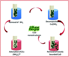
Superhydrophobic surfaces of CuO were synthesized using a successive ionic-layered adsorption reaction technique by varying the number of deposition cycles followed by a thermal annealing process. The prepared superhydrophobic surface was composed of monoclinic CuO, which was confirmed by X-ray diffraction and X-ray photoelectron spectroscopy. Dynamic contact angle measurements were obtained using a droplet evaporation method. The contact angles measured on CuO surfaces after 20, 40, and 60 deposition cycles were similar, all showing hydrophilicity. After the thermal treatment, the prepared films exhibit super-hydrophobicity with a high water contact angle of approximately 157°, which contributed to the stable superhydrophobic surface. A considerable increase in surface roughness (from 23.81 to 74.54 nm) and the conical-shaped CuO nanostructures led to super-hydrophobicity. Also a possible mechanism for the wettability behavior is proposed. Finally, the superhydrophobic CuO surface which was used for the detection of H2S gas showed a very fast response. These results indicate that the low temperature deposition of CuO nanostructured thin films were promising for reliable high-performance gas sensors.


Introduction

Extremely water repellent (superhydrophobic) surfaces have attracted considerable attention in the field of surface engineering because of their advantages in applications such as self-cleaning, drug delivery, anticorrosion, and lab-on-a-chip technology.1 In addition, hydrophobic interactions are of interest in biological systems, where they are essential for the formation of lipid bi-layer cell membranes in organisms. The lotus leaf has a distinct water repelling surface produced by its high roughness conical-shaped epidermal cell structures.2 On this basis, researchers have focused on the preparation of such surfaces using metals, metal oxides, polymers and natural materials. The roughness and morphology are promising factors for controlling the wettability of inorganic materials, which have been defined theoretically by Wenzel, and Cassie and Baxter.3,4 High roughness is achieved by patterning or coating different substrates with ligands or thiol modified surfaces. For example, the surfaces of glass, copper, gold, aluminum, and silica substrates have been successfully modified with octadecanethiol or dodecanoic acid to produce high roughness hydrophobic surfaces that prevent the adsorption of water droplets.5–7 In addition, micro/nanostructures bestow an excellent super-hydrophobicity and such surfaces are mostly manufactured using inorganic semiconductors because of their easy synthesis and controlled morphology. Cupric oxide (CuO) is becoming popular for industrial applications, as it is a non-toxic and abundant material. Although cupric oxide is a well-known hydrophilic material, it exhibits extreme water repulsion with a water contact angle (∼154° to 158°) after surface modification with octadecanethiol and fluoroalkylsilane.8 Without surface modification, such innovative superhydrophobic surfaces are difficult to produce.

In general, specialized equipment (e.g., spray pyrolysis) is needed to produce superhydrophobic surfaces.9 In the present work, superhydrophobic surfaces of CuO were prepared without surface modification or patterning, using the simple and cost-effective SILAR (successive ionic layer adsorption and reaction) process under mild reaction conditions. The unique part of this work is that the annealing process allows the formation of high roughness CuO films without oxidation, and producing novel superhydrophobic surfaces. CuO is a p-type semiconductor with a narrow energy bandgap (Eg = 1.2 eV),10 and surfaces of such material are very interesting for gas sensing, particularly for H2S detection. Since the high sensitivity of CuO nanoparticle-decorated SnO2 nanostructures for H2S detection was reported,11 CuO-based nanostructure sensors have been studied extensively for this application.10–17 Although, the sensitivity to H2S gas of such nanostructures is extremely high, the response time is slow. In this study, the sensing properties of a superhydrophobic surface of CuO towards H2S gas were examined and compared to those of CuO nanoparticle-decorated SnO2 nanostructures. A response of ∼34% with response and recovery times of 107 and 127 s towards 2 ppm H2S, respectively, at 200 °C were achieved, which are considerably shorter than those of CuO nanoparticle-decorated SnO2 nanostructures (response time = 150 s and recovery time = 2350 s).11

Experimental

Materials

Copper sulfate dihydrate (CuSO4·2H2O, Himedia, 99.9%, AR grade), 25% ammonia (NH3) solution (Himedia), and distilled water (DW) were used as received to prepare the superhydrophobic surfaces of CuO.

Design of superhydrophobic surfaces of CuO

Superhydrophobic surfaces of CuO nanostructures were prepared using a SILAR process as reported in a previous study for fabricating ZnO.18 In a typical procedure, CuSO4·2H2O was dissolved in diluted NH3 to form a copper ammonia complex solution, which acted as a cationic precursor. The SILAR growth process is a deposition cycle involving the alternate immersion of the substrate in cationic and anionic solutions interspersed with a rinse in double distilled (DD) water kept at room temperature. The substrate was first immersed in a beaker containing the cationic precursor for 40 s, resulting in the adsorption of the copper ammonia complex [(Cu(NH3)4)2+] onto the substrates due to the Van der Waals forces. Subsequent immersion of the substrate in DD water for 20 s resulted in the conversion of the adsorbed copper ammonia complex to copper hydroxide (Cu(OH)2). The Cu(OH)2 coated substrate was immersed in the anionic precursor (DW at 80 °C) for 60 s to convert the copper hydroxide (Cu(OH)2) molecules to CuO.19 Then the substrates were dipped into DD water to detach the loosely bonded molecules. A drying period of 20 s was used between each deposition cycle. Uniform CuO nanostructures were obtained by repeating the deposition (20, 40 or 60 cycles). Fig. 1 shows a schematic diagram of the preparation of the CuO nanostructures. The detailed chemical reactions involved in the SILAR growth process are as follows:
[Cu(NH3)4]2+ + H2O → Cu2+ + 4NH3 + OH

Cu2+ + 2OH → Cu(OH)2
 
Cu(OH)2 → CuO (s) + H2O (1)

image file: c6ra00209a-f1.tif
Fig. 1 Schematic diagram of the growth of CuO nanostructure thin films using the SILAR method.

Characterization techniques

X-ray diffraction (XRD, X'Pert PRO) of the prepared nanostructures was performed using filtered Cu-Kα radiation (λ = 1.5406 Å). X-ray photoelectron spectroscopy (XPS) was also performed (Kratos Analytical, ESCA-3400, Shimadzu). The spectra were corrected by −1.25 eV using the standard binding energy of the C–C bonds (C 1s, 284.6 eV) from surface contaminations. The surface morphologies of the samples were investigated using a field-emission scanning electron microscopy (FESEM, FEI Quanta-250). Atomic force microscopy (AFM, Veeco diCaliber) was performed in tapping mode. The water contact angle measurements were carried out using an FTA 188 video Tensiometer instrument.

Gas sensing

For the gas sensing tests, multiple electrically connected CuO thin film sensors were prepared. The CuO thin film samples were dispersed ultrasonically in a mixture of deionized water (5 ml) and isopropyl alcohol (5 ml). The samples were placed on 200 nm thick SiO2-coated Si (100) substrates equipped with pairs of interdigitated electrodes (IDE) Ni (∼200 nm)/Au (∼50 nm) with gaps of 20 μm. The flow-through technique was used to test the gas sensing properties. All measurements were performed in a temperature-stabilized sealed chamber with a constant gas flow rate of 200 cm3 min−1 at 100, 200, or 300 °C under 40% relative humidity (RH). The H2S concentration was controlled by mixing H2S gas with synthetic air at different ratios. The electrical resistances of the gas sensors were determined by measuring the electric current using a Keithley source meter-2612 with a source voltage of 1 V. Detailed procedures for the sensor fabrication and testing are described elsewhere.20

Results and discussion

Structural and surface analyses

The phase purity and crystallinity of the prepared CuO nanostructured thin films were analyzed by XRD. Fig. 2 shows the XRD patterns of the as-prepared and annealed samples from the different SILAR cycles. All the XRD peaks were easily indexed to the standard JCPDS (PDF#05-0661) file for CuO. The XRD patterns of the as-prepared and annealed thin films showed peaks from the monoclinic phase of crystalline CuO with (−111) and (111) lattice planes. No extra diffraction peaks were detected from copper hydroxide or cuprous oxide, clearly showing that CuO was the only crystalline material formed in the substrate. An increase in the peak intensity and decrease in peak widths of the nanostructured thin films was observed with increasing annealing temperature from 100–300 °C, indicating increasing crystallinity with annealing. Therefore, the annealing process and deposition cycle improved the crystallinity of the CuO thin films deposited on glass substrates using the SILAR method. The heat energy from the annealing process was available to form tight-packed and highly crystalline films.8 All the annealed samples showed improved crystallinity compared to that of the pure CuO, as confirmed by grain growth calculated using Scherrer's formula (as shown in Fig. 2d). The mean grain size increased from approximately 11 to 19 nm when the annealing temperature increased from 100 to 300 °C.
image file: c6ra00209a-f2.tif
Fig. 2 XRD pattern of the CuO nanostructured thin films (a) 20 cycles (b) 40 cycles (c) 60 cycles (d) average grain sizes of the thin films prepared at different deposition cycles.

The as-prepared and annealed CuO nanostructured thin films were analyzed by XPS to verify the surface composition of the film, and similar spectra were observed. Fig. 3 and 4 shows the peaks corresponding to Cu 3d, 3p, 3s, 2p, and O 1s. No peak shifts or unidentified peaks were observed. The C 1s peak was also observed, which was attributed to the exposure of the samples to air. The main peak of Cu (2p3/2), for both the as-prepared and annealed samples, was observed at a binding energy of 933.15 eV and assigned to Cu2+ ions, indicating the presence of CuO.21 In addition, the O (1s) peak was observed at a binding energy of 529.99 eV, which corresponds to CuO.22 Based on the phase diagram of CuO, it has a stable phase up to 300 °C.23 Hence, we can conclude that the prepared films are pure CuO.


image file: c6ra00209a-f3.tif
Fig. 3 XPS spectra of the as-prepared CuO thin films prepared at (a) 20, and (b) 60 deposition cycles, and (c) and (d) their corresponding magnified spectra.

image file: c6ra00209a-f4.tif
Fig. 4 XPS spectra of the annealed (at 300 °C) CuO thin films prepared at (a) 20, and (b) 60 deposition cycles, and (c) and (d) their corresponding magnified spectra.

The surface morphologies of the CuO films were analyzed by FESEM. Fig. 5(a–f) shows FESEM images of the CuO nanostructured thin films prepared at 20, 40 and 60 SILAR deposition cycles at two different magnifications. The CuO films grown at 20 deposition cycles had randomly distributed nano-spindles (Fig. 5b). These spindle-like structures were 300–400 nm in length and 100–200 nm in width. When the number of deposition cycles was increased to 40, the edges of the nano-spindles became longer and sharper (Fig. 5d). With further increases in the number of deposition cycles to 60, these spindles became denser. When the deposition cycles were increased, a larger number of spindles were formed as shown in Fig. 5f. Fig. 6 shows FESEM images of the films prepared at different deposition cycles and at three different annealing temperatures. With increasing annealing temperature of the films prepared at 20 deposition cycles, the spindles grew closer together and at 300 °C, they exhibited a flower-like structure. When the film was prepared at 40 cycles, flower-like morphology was obtained at 200 °C and it had the appearance of an aloe vera plant, different to that formed at 20 cycles. For the CuO films prepared at 60 cycles, a highly dense film of spindles was formed. In general, as the annealing temperature was increased the spindles grew closer to each other and formed a flower-like morphology. The CuO nanostructures were distributed over the entire area of the films with no porosity or agglomeration. As shown in the images, the films have good thickness uniformity, as well as a smooth and dense surface. Such surface morphologies consisting of spindles composed of nanosized features are similar to that observed on lotus leaves.2 The growth of CuO nanoflowers was attributed to the following mechanism. When water is used as a solvent, it tends to produce a large number of OH ions24 with the reaction with dilute ammonia. These OH ions combine with the Cu2+ ions and produce a spindle-like morphology. Owing to the polarity of the water, the spindles grow closer together as the deposition time increases.


image file: c6ra00209a-f5.tif
Fig. 5 FESEM images of the as-prepared CuO nanostructured thin films (a) and (b) 20 cycles (c) and (d) 40 cycles (e) and (f) 60 cycles.

image file: c6ra00209a-f6.tif
Fig. 6 FESEM images of CuO nanostructured thin films annealed at 100 °C for as prepared (a) 20 cycles (b) 40 cycles (c) 60 cycles and annealed at 200 °C for (d) 20 cycles (e) 40 cycles (f) 60 cycles similarly annealed at 300 °C for (g) 20 cycles (h) 40 cycles, and (i) 60 cycles.

Fig. 7 shows three-dimensional (3-D) AFM images of the CuO nanostructured thin films prepared at 20 deposition cycles and annealing temperatures of 100 °C or 300 °C. As shown in Fig. 7, the surface morphology of all the samples has a spindle-like morphology. When increasing the annealing temperature, the edges of the spindles become sharper and homogeneous. High-density spindles were observed when the annealing temperature was increased (Fig. 7b and c). The mean size distribution obtained from the histogram was 100–300 nm. The root-mean-square (RMS) surface roughness of the CuO thin films was obtained using the following equation.25

 
image file: c6ra00209a-t1.tif(2)
where N is the number of data points and rn is the surface height of the nth datum.


image file: c6ra00209a-f7.tif
Fig. 7 AFM images and their corresponding histograms of nanostructured CuO thin films prepared at 20 cycles (a–c) as prepared and annealed at (d–f) 100 °C and (g–i) 300 °C.

The observed root-mean-square surface roughness values were approximately 23.815 nm, 54.0721 nm and 74.5492 nm for the films as-prepared, annealed at 100 °C, and annealed at 300 °C, respectively. The films prepared with 20 deposition cycles exhibited a much smoother surface than the films annealed at 100 °C and 300 °C. Increased surface roughness of the CuO films was observed with increasing annealing temperature. Such a nanoscale structure can act as an excellent bio-inspired design for use as a hydrophobic surface.

Wettability of CuO nanostructured thin films

The wettability of the CuO films, both as prepared and annealed at different temperatures, was evaluated by measuring the water contact angle using the sessile drop method at ambient temperature. Water droplets of about 3 μL from a hydrophobized needle on a micro-syringe were dropped carefully onto the surfaces. The average WCA value was determined using image analysis software, SCA20, built up in this OCAM and a fitting strategy to the experimental drop profiles at five different positions for the sample. Fig. 8(a–e) shows the variation of the WCA of the CuO films with different deposition cycles and the mechanism behind the superhydrophobic nature of CuO. The as-prepared films showed a WCA value of 27o indicating super-hydrophilicity. When the films were annealed, the maximum WCA was approximately 157°, which indicates super-hydrophobicity. The WCA values (Fig. 8(b–e)) indicate that the wettability of the CuO films transforms from hydrophilicity to super-hydrophobicity as the annealing temperature is increased.
image file: c6ra00209a-f8.tif
Fig. 8 (a) Mechanism of the super-hydrophobicity of CuO thin films, water contact angles of CuO nanostructured thin films deposited at (b) 20 cycles (c) 40 cycles (d) 60 cycles and (e) plot of the contact angle vs. annealing temperatures.

Fig. 8a shows a schematic of the wettability gradient of the CuO surfaces with the contact angle illustrating the mechanism behind the transformation from superhydrophilic to superhydrophobic. Cassie and Baxter proposed that if the surface is rough enough, a large amount of air will be trapped at the interface between the water and the film surface.3,4 As observed in the FESEM and AFM images, the high roughness of the film maximizes the water contact angle. The films exhibit Cassie–Baxter wetting behavior because water droplets on the surface showed high hydrophobicity. The super-hydrophobicity of the CuO surfaces is attributed to the two main features observed from FESEM and AFM: (i) a surface morphology that imitates the lotus leaf and has conical shaped edges; and (ii) a high surface roughness from the CuO nanostructures which amplifies the hydrophobicity of the surface. In the present case, thermal annealing resulted in high surface roughness. The repulsion of water from a superhydrophobic surface also has the effect of limiting contact of any components in the water with the surface.

H2S gas sensing behavior

Here, the sensing characteristics of CuO nanostructured films were investigated using H2S gas, which is colorless, corrosive, and flammable, with the characteristic foul odor of rotten eggs. Fig. 9 shows the gas response transients of the CuO nanostructured thin film (60 deposition cycles) to H2S pulses for gas concentrations ranging from 0.1 to 10 ppm at 300 °C. The measured resistance increased for each H2S pulse and recovered completely to the initial value when the supply of H2S gas was stopped and the sample was exposed to air. Hence, the electrical responses of the CuO sensors were reversible and reproducible.
image file: c6ra00209a-f9.tif
Fig. 9 Gas response transients of a CuO nanostructured thin film (60 deposition cycles).

Fig. 10a shows the responses of the CuO thin film to H2S gas as a function of the H2S gas concentration. The response is defined as (RgRa)/Ra, where Rg and Ra are the electrical resistances of the sensors to H2S gas and air, respectively. The CuO thin film sensor exhibited a response of 2.8–37.7% to 0.1–10 ppm of H2S, respectively, at 300 °C. Fig. 10b shows the effect of the operating temperature on the response of the sensor to H2S gas. The CuO thin film sensors showed the strongest response at 200 °C. Oxygen molecules adsorbed on the surface of the CuO thin films form different oxygen ions depending on the working temperature. According to the literature, below 100 °C, O2 forms. In the temperature range of 100–300 °C, O forms, and O2− forms above 300 °C. In this study, the CuO sensor showed a relatively weak response at 100 °C due to the formation of O2. The response became stronger when the temperature was increased from 100 to 200 °C due to the formation of O. When the temperature was increased from 200 to 300 °C, the response of the CuO sensors decreased because of the formation of O2−. The decrease in the response of the sensor while increasing the temperature from 200 to 300 °C was attributed partly to the desorption of the adsorbed species at high temperature. As the strongest response was obtained at 200 °C, we conclude that this is the optimal working temperature for such a device.


image file: c6ra00209a-f10.tif
Fig. 10 (a) Gas response transients of the CuO thin film sensor at different temperatures, (b) response of the CuO thin film sensor as a function of temperature.

Fig. 11a shows the response time of the CuO thin film to H2S gas as a function of the H2S gas concentration. Fig. 11b shows the recovery time of the CuO thin film to H2S gas as a function of the H2S gas concentration. In this study, the response time and recovery time are defined as the times to achieve a 90% change in resistance upon exposure to H2S and air, respectively. Regarding the effect of the working temperature on the sensing speed of the CuO film, the fastest response and recovery was observed at 200 °C and 300 °C, respectively. In addition, the sensor showed the shortest sensing time (sum of the response time and recovery time) at 200 °C. However, the response and recovery times showed little dependence on the H2S concentration. The dependence of the response time and recovery time of the sensors on the working temperature could also be explained in a similar manner to the response transients. Different oxygen ion species form at different temperatures after the adsorption of oxygen molecules by the sensor surfaces and the reaction rate of H2S with O at 200 °C might be stronger than that of O2 at 100 °C or O2− at 300 °C, leading to the fastest sensing at 200 °C. As shown in Table 1, the CuO thin films synthesized in this study showed shorter sensing time towards H2S gas than other CuO or Cu-based sensors, even though the former showed slightly weaker response to H2S gas than the latter.


image file: c6ra00209a-f11.tif
Fig. 11 (a) Response time and (b) recovery time of the CuO nanostructure thin film sensor at different temperatures.
Table 1 Responses, response times and recovery times of the nanomaterial sensors showing high responses to H2S
Nanomaterials H2S conc. (ppm) Response time (s) Recovery time (s) Ref.
CuO thin films 10 71 133 Present work
SnO2 thin films with CuO islands 20 14 481 26
CuO-modified SnO2 nanoribbons 3 75 415 8
Cu-doped SnO2 nanowires 50 150 2350 11
Pt-doped SnO2 nanofibers 20 1 280 27
Pd-doped CuO nanorods 20 700 120 28


The sensing mechanism of the CuO sensors towards H2S gas can be explained as follows29,30 CuO is a p-type semiconductor and upon exposure to air, the CuO surface adsorbs oxygen readily and creates holes that form an accumulation layer at the CuO surface due to the following reaction:

 
1/2O2 (g) → O (ad) + h+ (3)

Upon exposure to low H2S concentrations, the following reaction occurs between H2S and the pre-adsorbed oxygen species at 300 °C:

 
2H2S (g) + 6O (ad) + 6h+ → 2H2O + 2SO2 (g) (4)

Upon exposure to high H2S concentrations, a CuS layer might form on the surface of the CuO sensor according to the following reaction:

 
CuO (g) + H2S (s) → CuS (s) + H2O (g) (5)

The formation of metallic CuS decreases the electrical resistance significantly. CuS formation has been reported previously.11–16 When the H2S gas supply is stopped, the CuS layer will be oxidized back to CuO by the following reaction:

 
2CuS3+ + 6O (ad) + 6h+ → 2CuO + 2SO2 (6)

Consequently, recovery of the resistance will occur.

Conclusions

A simple and cost effective SILAR process can produce a functional superhydrophobic CuO surface. Observed changes in surface roughness and morphology are attributed to the thermal annealing process, which contributed to the significant differences in contact angles. XRD and XPS confirmed that the prepared nanostructures were pure CuO and no oxidation process took place after annealing. The superhydrophobic surfaces of CuO was tested for H2S gas detection and a response of ∼34% with response and recovery times to 2 ppm H2S of 107 and 127 s, respectively, were achieved at 200 °C. These values are considerably shorter than those of CuO nanoparticle-decorated SnO2 nanostructures, which are known as excellent H2S gas sensing materials (response time of 150 s and recovery time of 2350 s). The superhydrophobic CuO surfaces demonstrated in this study also have potential applications in self-cleaning and water repelling surfaces.

Acknowledgements

This study was supported by Basic Science Research Program through the National Research Foundation of Korea (NRF) funded by the Ministry of Education (2010-0020163).

References

  1. W. Barthlott and C. Neinhuis, Planta, 1997, 202, 1 CrossRef CAS.
  2. Z. Burton and B. Bhushan, Ultramicroscopy, 2006, 106, 709 CrossRef CAS PubMed.
  3. R. N. Wenzel, Ind. Eng. Chem., 1936, 28, 988 CrossRef CAS.
  4. A. B. D. Cassie and S. Baxter, Trans. Faraday Soc., 1944, 40, 546 RSC.
  5. B. Wang, J. Li, G. Wang, W. Liang, Y. Zhang, L. Shi, Z. Guo and W. Liu, ACS Appl. Mater. Interfaces, 2013, 5, 1827 CAS.
  6. G. Wang and T. Y. Zhang, ACS Appl. Mater. Interfaces, 2012, 4, 273 CAS.
  7. S. Barthwal, Y. S. Kim and S. H. Lim, Int. J. Precis. Eng. Manuf., 2012, 13, 1311 CrossRef.
  8. X. Liu, Z. Jiang, J. Li, Z. Zhang and L. Ren, Surf. Coat. Technol., 2010, 204, 3200 CrossRef CAS.
  9. S. S Latthe, P. Sudhagar, C. Ravidhas, A. J. Christy, D. D. Kirubakaran, R. Venkatesh, A. Devadoss, C. Terashima, K. Nakata and A. Fujishima, CrystEngComm, 2015, 17, 2624 RSC.
  10. J. Chen, K. Wang, L. Hartman and W. Zhou, J. Phys. Chem. C, 2008, 112, 16017 CAS.
  11. X. Kong and Y. Li, Sens. Actuators, B, 2005, 105, 449 CrossRef CAS.
  12. I. Hwang, J. Choi, S. Kim, K. Dong, J. Kwon, B. Ju and J. Lee, Sens. Actuators, B, 2009, 142, 105 CrossRef CAS.
  13. X. Xue, L. Xing, Y. Chen, S. Shi, Y. Wang and T. Wang, J. Phys. Chem. C, 2008, 112, 12157 CAS.
  14. A. Chowdhuri, V. Gupta, K. Sreenivas, R. Kumar, S. Mozumdar and P. Patanjali, Appl. Phys. Lett., 2004, 84, 1180 CrossRef CAS.
  15. L. Patil and D. Patil, Sens. Actuators, B, 2007, 122, 357 CrossRef.
  16. F. Shao, M. Hoffmann, J. Prades, R. Zamania, J. Arbiolc, J. Orante, E. Varechkina, M. Rumyantseva, A. Gaskov, I. Giebelhaus, T. Fischer, S. Mathur and F. Hernandez-Ramirez, Sens. Actuators, B, 2013, 181, 130 CrossRef CAS.
  17. S. Park, S. Kim, H. Ko and C. Lee, Appl. Phys. A, 2014, 117, 1259 CrossRef CAS.
  18. P. Suresh Kumar, A. D. Raj, D. Mangalaraj and D. Nataraj, Appl. Surf. Sci., 2008, 255, 2382 CrossRef.
  19. M. Basu, A. K. Sinha, M. Pradhan, S. Sarkar, Y. Negishi and T. Pal, J. Phys. Chem. C, 2011, 115, 20953 CAS.
  20. S. Park, S. An, Y. Mun and C. Lee, ACS Appl. Mater. Interfaces, 2013, 5, 4285 CAS.
  21. F. Shi and C. Cui, Inorg. Mater., 2010, 46, 565 CrossRef CAS.
  22. C. Plackowski, M. A. Hampton, A. V. Nguyen and W. J. Bruckard, Langmuir, 2013, 29, 2371 CrossRef CAS PubMed.
  23. M. F. Alkuhaili, Vacuum, 2008, 82, 623 CrossRef CAS.
  24. T. H. Tran and V. T. Nguyen, Int. Scholarly Res. Not., 2014, 2014, 1 CrossRef.
  25. K. Miyoshi and Y. W. Chung, Surface diagnostics in tribology: fundamental principles and Applications, World scientific publishing, 1993, p. 75 Search PubMed.
  26. J. Y. Park, S.-W. Choi, J. W. Lee, C. Lee and S. S. Kim, J. Am. Ceram. Soc., 2009, 92, 2551 CrossRef CAS.
  27. A. Kolmakov, Y. Zhang, G. Cheng and M. Moskovits, Adv. Mater., 2003, 15, 997 CrossRef CAS.
  28. Q. Wan and T. H. Wang, Chem. Commun., 2005, 30, 3841 RSC.
  29. H. Kim, C. Jin, S. Park, S. Kim and C. Lee, Sens. Actuators, B, 2012, 161, 594 CrossRef CAS.
  30. N. Yamazoe and K. Shimanoe, Sens. Actuators, B, 2010, 150, 132 CrossRef CAS.

This journal is © The Royal Society of Chemistry 2016