 Open Access Article
Creative Commons Attribution 3.0 Unported Licence
Metal nanoparticles reveal the organization of single-walled carbon nanotubes in bundles†
Raul D.
Rodriguez
*ab,
Thomas
Blaudeck
*c,
Jana
Kalbacova
ab,
Evgeniya
Sheremet
d,
Steffen
Schulze
d,
David
Adner
e,
Sascha
Hermann
bc,
Michael
Hietschold
d,
Heinrich
Lang
be,
Stefan E.
Schulz
bcf and
Dietrich R. T.
Zahn
ab
aSemiconductor Physics, Technische Universität Chemnitz, 09107 Chemnitz, Germany. E-mail: raul.rodriguez@physik.tu-chemnitz.de
bCenter for Advancing Electronics Dresden (cfaed), Technische Universität Chemnitz, 09107, Chemnitz, Germany
cCenter for Microtechnologies, Technische Universität Chemnitz, 09107 Chemnitz, Germany. E-mail: thomas.blaudeck@zfm.tu-chemnitz.de
dSolid Surfaces Analysis, Technische Universität Chemnitz, 09107 Chemnitz, Germany
eInorganic Chemistry, Technische Universität Chemnitz, 09107 Chemnitz, Germany
fFraunhofer Institute for Electronic Nano Systems (Fraunhofer ENAS), 09126 Chemnitz, Germany
First published on 26th January 2016
Abstract
Single-walled carbon nanotubes (SWCNTs) were decorated with metal nanoparticles. Using a complementary analysis with spatially resolved micro-Raman spectroscopy, high resolution transmission electron microscopy, electron diffraction, and tip-enhanced Raman spectroscopy, we show that the SWCNTs form bundles in which smaller diameter SWCNTs are the ones preferentially affected by the presence of Au and Ag nanoparticles. This result is exploited to evaluate the structural organization of SWCNTs with mixed chiralities in bundles, leading us to postulate that smaller diameter SWCNTs surround larger ones. We found that this effect occurs for very distinct scenarios including SWCNTs both in nanometer thin films and in field effect transistor configurations at the wafer-level, suggesting a universal phenomenon for SWCNTs deposited from dispersions.
Introduction
Single-walled carbon nanotubes (SWCNTs) have remarkable properties that render them ideal nanoelectronic constituents1 for technological applications, e.g. in high-frequency electronics2–4 and sensorics.5–7 The conceived components comprise transistors with channels formed by ultra-dense SWCNT arrays2,4,5 or networks,3,5,6 or based on individualized (i.e., de-bundled) SWCNTs.5,7,8 Recently, these developments led to the construction of an entire computer.9 Additional device functionality and enhanced performance could be accomplished by decorating SWCNTs with plasmonic nanoparticles for optoelectronic applications.10 The idea is that coupling light with metal nanoparticles would induce electron transfer to or from the SWCNT due to the plasmonic excitation thus changing the transfer characteristics of the SWCNT field-effect transistor (CNT-FET).11,12 With Raman spectroscopy we discovered that nanoparticles on SWCNT films and CNT-FETs affect particular carbon nanotube chiralities. In view of this observation, we investigated the possibility to probe the outer shells of bundles by analyzing the influence of metal nanoparticles on their Raman spectra. The chirality of a nanotube determines its fundamental physical properties, and the knowledge of it allows a realistic simulation of SWCNT and a proper comparison to experimental results.13 From the chemical and functionalization point of view, being able to identify which nanotubes lay at the outer layer of bundles is an important achievement since these SWCNTs are the ones directly interacting with the environment. Moreover, this information is critical for device functionalization, e.g. engineering of SWCNT devices for sensing applications.14,15Experimental methods
In our study, we experimentally compare the Raman spectra of (i) aligned SWCNT films in CNT-FET device geometry and (ii) SWCNT network films both (a) in the pristine state and (b) decorated with metal nanoparticles. Two different functionalization protocols, i.e. microfluidic decoration (case i) and electrochemical deposition (case ii) were employed to exclude chemical effects. Au and Ag nanoparticles were selected on the basis of established decoration protocols. Both metal systems are plasmon-active under light excitation in the visible range.16In the CNT-FETs used in this study, the source/drain patterns were produced using standard microfabrication techniques. In this transistor configuration, a back-gate electrode is formed by the p-doped silicon substrate. In detail, the silicon wafers (p-type, (100); e.g. Si-Mat 044GN1, MEMC) with 200 nm thermal oxide, were cleaned and metallized with a sophisticated pattern of Pd electrodes (width: 2 μm, gap distance: 0.8–1.6 μm). The sequence of standard microfabrication techniques further comprised wet cleaning, annealing, photolithography, dry etching, oxidation, wet etching, HF etching, Al sputtering, Pd electron beam deposition, and lift off.17 The individual or small-bundled SWCNTs were deposited and electrokinetically aligned between the electrodes18,20 and consequently functionalized19 to form a tunable transistor channel. The deposition and alignment of the SWCNTs were performed from aqueous dispersions of SWCNTs (Nanointegris Inc., >98% semiconducting, length ca. 2 μm) prepared according to a previous protocol including homogenization and debundling in sodium dodecyl sulfate (SDS, Sigma Aldrich, ACS/BioXtra grade or comparable) dissolved in deionized water (18 MΩ cm), followed by ultrasonication (Sonotrode KE76, Bandelin) and centrifugation (2 h at 55![[thin space (1/6-em)]](https://www.rsc.org/images/entities/char_2009.gif) 000g).20 For functionalization of CNT-FETs at the wafer level, Au nanoparticles were synthesized according to the procedure by Lang and co-workers19,21 and for deposition a soft organosilicon stamp with a channel-like opening towards the silicon wafer was aligned over the CNT-FET structures and supplied with microfluidic tubing. A microsyringe pump with a controllable flow rate of a few to several hundred μL per minute was used to guide the dispersion of Au nanoparticles over the CNT-FETs.19
000g).20 For functionalization of CNT-FETs at the wafer level, Au nanoparticles were synthesized according to the procedure by Lang and co-workers19,21 and for deposition a soft organosilicon stamp with a channel-like opening towards the silicon wafer was aligned over the CNT-FET structures and supplied with microfluidic tubing. A microsyringe pump with a controllable flow rate of a few to several hundred μL per minute was used to guide the dispersion of Au nanoparticles over the CNT-FETs.19
The SWCNT films were produced according to the procedure reported by Wu et al.22 High-resolution transmission electron microscopy (HRTEM) was performed on several SWCNT bundles prepared from liquid dispersions dried on a carbon-coated copper grid. A Philips CM20FEG electron microscope with Schottky emitter was operated at 200 kV for imaging and electron diffraction. Scanning electron microscopy measurements were performed using a NovaNanoSEM 200 microscope from FEI. The SWCNT film was transferred to a mica substrate with an evaporated layer of gold (ca. 100 nm). The Kataura plot was adapted from literature,23,24 and updated with experimental data acquired using two Raman spectrometers, Dilor XY with Kr+ laser lines and a LabRam HR800 with 325.0, 514.7, and 632.8 nm excitation laser lines. The characterization of CNT-FET structures was carried out with a Horiba Raman Spectrometer LabRam HR800 with 100× objective (N.A. 0.9). Diffraction gratings of 600 l mm−1 and 2400 l mm−1 provide a spectral resolution experimentally determined of 3.1 and 0.8 cm−1, respectively under λ = 514.7 nm. Raman spectroscopy and Raman imaging were performed using a solid state laser with 514.7 nm wavelength.
Ag nanoparticles were electrochemically grown on a SWCNT film under a bias of 1 V, with an Au coil acting as a counter electrode, and an aqueous solution of AgNO3 as the Ag source.
Tip-enhanced Raman spectroscopy (TERS) experiments were performed in side-illumination/side-collection configuration (Agilent 5420 AFM coupled to a LabRam spectrometer). The electrochemically sharpened Ag tips and setup used were described previously.25
Results and discussion
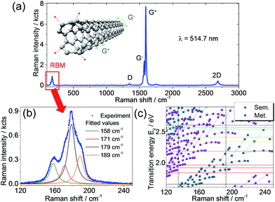
When SWCNTs stretch radially due to lattice vibrations a band appears in the Raman spectra in the low frequency range (typically 100–400 cm−1). This is the so-called radial breathing mode (RBM) shown in the Raman spectrum in Fig. 1a and b. The tube diameter is inversely proportional to the Raman shift of the RBM (the higher the Raman shift, the lower the tube diameter and vice versa). In addition to the RBM region, Fig. 1a shows the higher-frequency Raman modes that are typical for SWCNTs.26 The D band around 1350 cm−1 only appears when defects are present.27 The G band is characteristic for all carbon materials with sp2 hybridization. This band around 1590 cm−1 splits into two, G− and G+ in carbon nanotubes due to the tube curvature that gives rise to longitudinal optical (LO) and transverse optical (TO) phonons for vibrations along and across the tube axis, respectively.28 The intensity ratio (i.e. the peak maxima) between the D and G bands gives an indication of defect concentration. The 2D band around 2700 cm−1, also known as G′, provides information on doping due to its high sensitivity to perturbations of the SWCNT electronic structure.28A very significant part of the Raman spectra and the most important for this work concerns the RBM region. The analysis of the RBM bands under different excitation wavelengths provides information on the carbon nanotube chiralities and chirality families related to the electronic transition energies (Eii) under resonance conditions.29 A complete picture of the optical transition energies of the SWCNTs and their dependence on diameter and chirality can be given in form of a Kataura plot.30Fig. 1c shows such a plot depicting the transition energies as a function of the Raman shift, with semiconducting and metallic SWCNT families indicated by circles and squares, respectively. By using different laser excitations that matched the optical transitions we were able to complement the theoretical Kataura plot with our experimental values. The laser excitations used in our work are indicated in Fig. 1c by horizontal colour lines matching a given SWCNT electronic transition, Eii. The fulfillment of this resonance condition leads to the appearance of RBM peak(s) in the Raman spectra at defined wavenumbers, like the four bands deconvoluted in Fig. 1b. Due to small phonon softening in metallic tubes (but not for semiconducting ones), the RBM position is only weakly affected by external parameters such as temperature, pressure, or environment.31 We would like to stress here that in this study, we employed a laser line which is in resonance solely with semiconducting SWCNTs and, thus, do not expect to observe any shift of the RBMs. In contrast, the RBM intensity is highly sensitive to external changes and the CNT environment due to the coupling of RBM with electronic transition energies Eii.
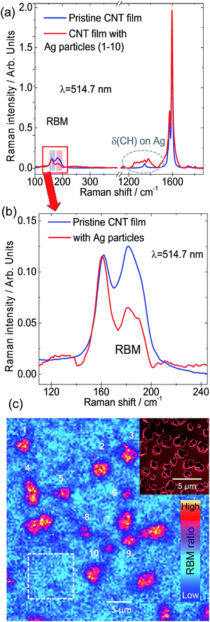
It is already well-known from Dai, Smalley, and co-workers32 that SWCNTs form superstructures such as solids, fibers, ropes, or bundles. They can comprise 100 to 500 individual SWCNTs, arranged in quasi-one-dimensional triangular arrays with a hexagonal lattice constant.32 However, this aggregate formation is often considered detrimental as it limits, for instance, the performance of the SWCNT devices. The particular internal structure of these superstructures, i.e. SWCNT morphology and the spatial location of different SWCNT chiralities in the bundle, were not explored until now. The reasons for this open issue are related to the limitations of current analytical methods. In general, bundles of nanotubes can be treated as a colloidal system, for which coagulation, i.e. the aggregate formation of its constituents, is driven by the relative interplay between attractive van der Waals interactions and repulsive barrier mechanisms, e.g. electrostatic interactions.8 In order to improve this situation and provide unprecedented insights on the bundle morphology, we combined different analytical methods that together offer complementary information on the bundle structure of SWCNTs. In particular, we expect that the tubes lying on the outer shell of the bundle will be mostly affected by the change of environment, i.e. the RBM intensity obtained from Raman analysis will change. Therefore, the analysis of RBM intensity changes upon decoration with metal nanoparticles gives an indirect way to determine which SWCNTs are located at the outer layers. Notably, we found that the SWCNTs arrangement in bundles is not random. Fig. 2 shows the micro-Raman spectroscopy analysis of a SWCNT film functionalized with electrochemically grown Ag nanoparticles. Here we used samples with electrochemically grown metal nanoparticles on SWCNT networks as a reference system since this approach excludes the influence of additional solvents involved in the microfluidic deposition. We relied on Ag nanoparticles in favour of Au as the protocol for electrochemical deposition of Ag particles is better established in our group33 and both material systems show a significant plasmonic response in the visible range. Fig. 2a shows the average Raman spectra over two different regions, with and without Ag particles. A zoom-in of the RBM range is shown in Fig. 2b. The RBM intensity ratio map presented in Fig. 2c was obtained from the bands marked by rectangles in Fig. 2a (zoomed in Fig. 2b), in the spectral ranges 156–164 cm−1 and 177–188 cm−1.
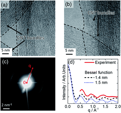
These RBM frequency regions correspond to SWCNTs with diameters between 1.5–1.6 nm and 1.3–1.4 nm, respectively. The different regions are indicated in the Raman map of the RBM intensity ratio in Fig. 2c, where the Ag clusters are numbered from 1 to 10, while the particle-free pristine region is indicated by the white dashed frame. The characteristic Ag nanoparticles observed by SEM on a Pt film are shown as an inset in Fig. 2c. It is evident from Fig. 2b that the intensity of RBM bands at higher frequency decreases after Ag particle functionalization. The contrast increase at the Ag clusters in the RBM intensity ratio map in Fig. 2c clearly reveals the selective modification of specific SWCNTs. By employing the Kataura plot (Fig. 1c), we can deduce which chirality families correspond to those RBM bands with decreased intensity. The intensity of bands above 170 cm−1 decreased when in contact with Ag particles, while SWCNTs with RBMs below 170 cm−1 retained their intensity relative to the G+ band. The two possible explanations for this effect are either (i) that there is a change in the dielectric constant of the environment after metal nanoparticle functionalization or (ii) that the silver nanoparticles induce charge transfer to/from the SWCNT and the plasmonic nanoparticles. Atomic force microscopy and electron microscopy and electron diffraction observations show that the SWCNTs in films arrange in bundles. Therefore, these results imply that those SWCNTs affected by Ag nanoparticles are located at the outer shell of bundles screening the SWCNTs at the core. This interpretation is coherent with high-resolution transmission electron microscopy (HRTEM) and electron diffraction results shown in Fig. 3.
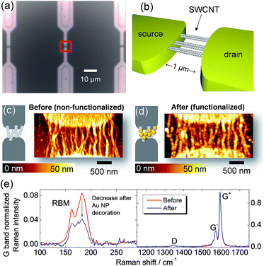
Fig. 3a and b show HRTEM images of SWCNTs deposited from dispersion on a carbon grid; the CNT bundle formation is directly verified at this resolution. The electron diffraction presented in Fig. 3c was obtained from an area of 170 × 170 nm2. The in-plane reflections from the 2D carbon lattice result in the maxima observed at 29.5 nm−1, 51.1 nm−1, and 58.7 nm−1 along the bundle axis (Fig. 3c and d).34 The intensity distribution I(q) in the diffraction pattern of a single SWCNT perpendicular to the fiber axis depends on the tube diameter according to I(q) ∼ (J0(qr))2, with J0 being the zero-order Bessel function.34,35Fig. 3d shows the intensity distribution perpendicular to the bundle axis determined from the experimental data in comparison with calculations of the Bessel distributions for SWCNTs with 1.4 nm and 1.5 nm diameters. In this way a good agreement is found that also verifies the Raman results. In conclusion of these findings, the HRTEM and electron diffraction observations confirm that the SWCNT form bundles and that these can be modeled as composed of SWCNT with diameters from 1.4 to 1.5 nm. Going beyond SWCNT films, we extended this analysis to SWCNTs integrated horizontally at the device level to investigate the bundle structure. The CNT-FET structure shown as an optical image in Fig. 4a and as a schematic drawing in Fig. 4b was characterized with atomic force microscopy (AFM), scanning electron microscopy (SEM), and micro-Raman spectroscopy before and after decoration with gold nanoparticles. The AFM observations of the device before and after functionalization in Fig. 4c and d show the successful decoration of the SWCNT by Au nanoparticles. We also observed that the nanoparticles attach preferentially to the SWCNT bundles rather than to the SiO2 substrate or Pd electrodes (Fig. 4d).18 This effect can possibly be ascribed to the interaction between Au and the remaining surfactant molecules on SWCNTs but is currently subject of further investigations.
The Raman spectra of the same device before and after functionalization are shown in Fig. 4e. Usual procedures for functionalization of graphene or carbon nanotubes have the drawback of introducing defects. However, a significant result of the present work is the negligible change in defect concentration after functionalization as evidenced by a constant D/G bands intensity ratio.
In the RBM region, we observe the overall intensity decrease of all modes. This overall intensity decrease can be attributed to the physical screening of SWCNTs by Au nanoparticles. Similarly, for the case of thin films, in Fig. 4e we also observe the selective decrease in the RBM intensity around 180 cm−1 for the CNT-FET device functionalized with Au nanoparticles.
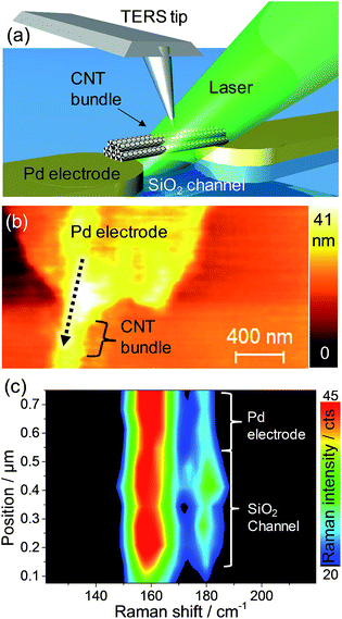
This plasmonic effect is expected to play an important role, especially in the case of Au nanoparticles where the plasmon resonance closely matches the laser excitation used (see ESI†). In order to rule out one of the mechanisms, the effect of a localized interaction was investigated using tip-enhanced Raman spectroscopy (TERS). We consider that a TERS tip (apex: 20–50 nm) interacting with aligned but non-functionalized SWCNTs in CNT-FET geometry makes a model for a hybrid system consisting of a plasmonic nanoparticle and a SWCNT bundle. The TERS tip in AFM even allows controlling the local interaction with SWCNT at the nanometer scale.36 The RBM region was mapped in TERS over the non-functionalized CNT-FET device as shown schematically in Fig. 5a. We observe noticeable changes in the RBM intensity in TERS at the interface between the Pd electrode and the SiO2 channel. The AFM image of the structure measured in TERS along with the direction and region of the line scan is shown in Fig. 5b. The TERS result in Fig. 5c shows that the change in environment between the Pd electrode and the SiO2 channel has a similar impact on the RBM intensity as do metal nanoparticles in the results discussed above. This result can occur as a direct effect of dielectric function change on RBM intensity or the effect of the substrate dielectric function on the intensity of the electric field created at the Ag tip apex due to an image dipole effect. The first one is the most likely reason behind the RBM changes in TERS since the change of electric field due to different substrate (Pd vs. SiO2) would affect the whole volume of the bundle rather than only the outer layer. Notice that in the TERS results in Fig. 5c the RBM intensity ratio is much lower than in the micro-Raman experiments shown in Fig. 4e. This difference is due to the continuous and strong interaction between metallic tip and CNT bundle that changes the resonance conditions of smaller diameter SWCNT.
The micro- and nano-Raman spectroscopy results are consistent with the interpretation that a particular CNT chirality is affected by the change in local environment. Therefore, we expect that those SWCNTs at the outer shell will be more affected by the environment change compared to those located at the inner shell. From these experimental observations we deduce that small diameter SWCNTs constitute the outer shell of bundles, while SWCNTs with larger diameters remain located in the bundle core. From the analysis of the RBM bands affected by Au nanoparticles, and with the aid of the Kataura plot in Fig. 1c, we can identify the possible SWCNT chiralities as (22, 2) and (21, 2), as well as others with diameters in the range of 1.2–1.6 nm. This result has significant implication on the functionalization of SWCNT-FET since any chemical processing, functionalization, and doping can be targeted specifically to those chiralities. It also implies that, when modeling the CNT–electrode interfaces, these ones are the SWCNT chiralities responsible for contact resistance and Schottky barriers.
Conclusions
In summary, decoration of single-walled carbon nanotubes (SWCNTs) with metal nanoparticles was conducted for SWCNT network films and SWCNT wafer-level field-effect transistors. HRTEM and electron diffraction show the formation of bundles that can be described by SWCNTs with a diameter distribution of 1.4 and 1.5 nm. Resonance Raman spectroscopy verifies the coexistence of several chirality families with nominal diameters varying in the range between 1.2 and 1.6 nm. Changes in the intensity of radial breathing modes before and after functionalization demonstrate that some specific SWCNT are most affected by Ag and Au nanoparticles. These SWCNT correspond to those with the smaller diameters in the bundle. We attribute the change in RBM intensities to the environmental change induced by the SWCNT-nanoparticle interaction. This hypothesis is supported by TERS results showing that different environments at the Pd/SiO2 interface also contribute to changes in RBM for SWCNT with the smaller diameter. The methodology demonstrated here allows a rapid and convenient identification of the SWCNTs located at the outmost bundle layers, which ultimately determine the device properties. The systematic investigation of different scenarios for which changes in RBM were observed: SWCNT film/Ag nanoparticles, SWCNT-FET with Au nanoparticles, and SWCNT-FET with a single Ag particle in the form of a TERS tip demonstrate a universal arrangement for bundles formed from dispersions. Our results open now a new question: what is the driving force that makes SWCNTs aggregate in the way evidenced in this work?Acknowledgements
We thank Parisa Bayat for performing the AFM measurements of the SWCNT-FETs. This work was supported by the DFG Cluster of Excellence “Center for Advancing Electronics Dresden” (cfaed), DFG Research Unit FOR1713. This work was performed in the context of the European COST Action MP1302 Nanospectroscopy.References
- A. Javey, M. Shim and H. Dai, Appl. Phys. Lett., 2002, 80, 1064–1066 CrossRef CAS.
- C. Rutherglen, D. Jain and P. Burke, Nat. Nanotechnol., 2009, 4, 811–819 CrossRef CAS PubMed.
- J. Vaillancourt, H. Zhang, P. Vasinajindakaw, H. Xia, X. Lu, X. Han, D. C. Janzen, W.-S. Shih, C. S. Jones and M. Stroder, Appl. Phys. Lett., 2008, 93, 243301 CrossRef.
- M. Steiner, M. Engel, Y.-M. Lin, Y. Wu, K. Jenkins, D. B. Farmer, J. J. Humes, N. L. Yoder, J.-W. T. Seo and A. A. Green, Appl. Phys. Lett., 2012, 101, 053123 CrossRef.
- S. Liu, Q. Shen, Y. Cao, L. Gan, Z. Wang, M. L. Steigerwald and X. Guo, Coord. Chem. Rev., 2010, 254, 1101–1116 CrossRef CAS.
- K. Melzer, V. D. Bhatt, T. Schuster, E. Jaworska, K. Maksymiuk, A. Michalska, P. Lugli and G. Scarpa, IEEE Sens. J., 2015, 15, 3127–3134 CrossRef CAS.
- T. Helbling, R. Pohle, L. Durrer, C. Stampfer, C. Roman, A. Jungen, M. Fleischer and C. Hierold, Sens. Actuators, B, 2008, 132, 491–497 CrossRef CAS.
- M. S. Amara, S. p. Rouzière, E. Paineau, M. Bacia-Verloop, A. Thill and P. Launois, J. Phys. Chem. C, 2014, 118, 9299–9306 CAS.
- M. M. Shulaker, G. Hills, N. Patil, H. Wei, H.-Y. Chen, H.-S. P. Wong and S. Mitra, Nature, 2013, 501, 526–530 CrossRef CAS PubMed.
- J. M. Lee, J. Lim, N. Lee, H. I. Park, K. E. Lee, T. Jeon, S. A. Nam, J. Kim, J. Shin and S. O. Kim, Adv. Mater., 2015, 27, 1519–1525 CrossRef CAS PubMed.
- A. Manjavacas, J. G. Liu, V. Kulkarni and P. Nordlander, ACS Nano, 2014, 8, 7630–7638 CrossRef CAS PubMed.
- Z. Li, Y. Xiao, Y. Gong, Z. Wang, Y. Kang, S. Zu, P. M. Ajayan, P. Nordlander and Z. Fang, ACS Nano, 2015, 9, 10158–10164 CrossRef CAS PubMed.
- E. C. Neyts, Y. Shibuta, A. C. T. van Duin and A. Bogaerts, ACS Nano, 2010, 4, 6665–6672 CrossRef CAS PubMed.
- P. Qi, O. Vermesh, M. Grecu, A. Javey, Q. Wang, H. Dai, S. Peng and K. J. Cho, Nano Lett., 2003, 3, 347–351 CrossRef CAS.
- S. Liu and X. F. Guo, NPG Asia Mater., 2012, 4, 1–10 CrossRef.
- C. Tserkezis, R. W. Taylor, J. Beitner, R. Esteban, J. J. Baumberg and J. Aizpurua, Part. Part. Syst. Charact., 2014, 31, 152–160 CrossRef CAS.
- S. Hermann, H. Fiedler, Y. Haibo, S. Loschek, J. Bonitz, S. E. Schulz and T. Gessner, Systems, Signals and Devices (SSD), 9th International Multi-Conference, 2012, pp. 1–5 Search PubMed.
- H. Yu, S. Hermann, Z. Dong, J. Mai, W. J. Li and S. E. Schulz, Sens. Actuators, A, 2013, 201, 36–42 CrossRef CAS.
- T. Blaudeck, D. Adner, S. Hermann, H. Lang, T. Gessner and S. E. Schulz, Microelectron. Eng., 2015, 137, 135–140 CrossRef CAS.
- R. D. Rodriguez, M. Toader, S. Hermann, E. Sheremet, S. Müller, O. D. Gordan, H. Yu, S. E. Schulz, M. Hietschold and D. R. T. Zahn, Nanoscale Res. Lett., 2012, 7, 1–6 CrossRef PubMed.
- A. Tuchscherer, D. Schaarschmidt, S. Schulze, M. Hietschold and H. Lang, Dalton Trans., 2012, 41, 2738–2746 RSC.
- Z. Wu, Z. Chen, X. Du, J. M. Logan, J. Sippel, M. Nikolou, K. Kamaras, J. R. Reynolds, D. B. Tanner and A. F. Hebard, Science, 2004, 305, 1273–1276 CrossRef CAS PubMed.
- A. Jorio, M. S. Dresselhaus, R. Saito and G. Dresselhaus, Raman spectroscopy in graphene related systems, John Wiley & Sons, 2010 Search PubMed.
- J. Maultzsch, H. Telg, S. Reich and C. Thomsen, Phys. Rev. B: Condens. Matter Mater. Phys., 2005, 72, 205438 CrossRef.
- R. D. Rodriguez, E. Sheremet, S. Müller, O. Gordan, A. Villabona, S. Schulze, M. Hietschold and D. R. T. Zahn, Rev. Sci. Instrum., 2012, 83, 123708 CrossRef CAS PubMed.
- M. S. Dresselhaus, G. Dresselhaus and M. Hofmann, Vib. Spectrosc., 2007, 45, 71–81 CrossRef CAS.
- M. M. Lucchese, F. Stavale, E. H. M. Ferreira, C. Vilani, M. V. O. Moutinho, R. B. Capaz, C. A. Achete and A. Jorio, Carbon, 2010, 48, 1592–1597 CrossRef CAS.
- M. S. Dresselhaus, A. Jorio and R. Saito, in Annual Review of Condensed Matter Physics, ed. J. S. Langer, 2010, vol. 1, pp. 89–108 Search PubMed.
- Q. Cheng, S. Debnath, E. Gregan and H. J. Byrne, Appl. Phys. A: Mater. Sci. Process., 2011, 102, 309–317 CrossRef CAS.
- H. Kataura, Y. Kumazawa, Y. Maniwa, I. Umezu, S. Suzuki, Y. Ohtsuka and Y. Achiba, Synth. Met., 1999, 103, 2555–2558 CrossRef CAS.
- H. Farhat, H. Son, G. G. Samsonidze, S. Reich, M. Dresselhaus and J. Kong, Phys. Rev. Lett., 2007, 99, 145506 CrossRef CAS PubMed.
- A. Thess, R. Lee, P. Nikolaev, H. Dai, P. Petit, J. Robert, C. Xu, Y. H. Lee, S. G. Kim and A. G. Rinzler, Science, 1996, 273, 483–487 CAS.
- L. Mikoliunaite, R. D. Rodriguez, E. Sheremet, V. Kolchuzhin, J. Mehner, A. Ramanavicius and D. R. T. Zahn, Sci. Rep., 2015, 5, 13150 CrossRef CAS PubMed.
- A. A. Lucas and P. Lambin, Rep. Prog. Phys., 2005, 68, 1181 CrossRef CAS.
- H. Jiang, A. G. Nasibulin, D. P. Brown and E. I. Kauppinen, Carbon, 2007, 45, 662–667 CrossRef CAS.
- P. Verma, T. Ichimura, T. Yano, Y. Saito and S. Kawata, Laser Photonics Rev., 2010, 4, 548–561 CrossRef CAS.
Footnote |
| † Electronic supplementary information (ESI) available. See DOI: 10.1039/c5ra28181d |
| This journal is © The Royal Society of Chemistry 2016 |

