Dzung Viet Dao†
*ab,
Hoang-Phuong Phan†*a,
Afzaal Qamara and
Toan Dinha
aQueensland Micro- and Nanotechnology Centre, Griffith University, Queensland, Australia. E-mail: d.dao@griffithuni.edu.au; hoangphuong.phan@griffithuni.edu.au
bSchool of Engineering, Griffith University, Queensland, Australia
First published on 12th February 2016
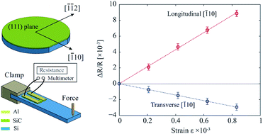
This paper presents for the first time the effect of strain on the electrical conductivity of p-type single crystalline 3C–SiC grown on a Si (111) substrate. 3C–SiC thin film was epitaxially formed on a Si (111) substrate using the low pressure chemical vapor deposition process. The piezoresistive effect of the grown film was investigated using the bending beam method. The average longitudinal gauge factor of the p-type single crystalline 3C–SiC was found to be around 11 and isotropic in the (111) plane. This gauge factor is 3 times smaller than that in a p-type 3C–SiC (100) plane. This reduction of the gauge factor was attributed to the high density of defects in the grown 3C–SiC (111) film. Nevertheless, the gauge factor of the p-type 3C–SiC (111) film is still approximately 5 times higher than that in most metals, indicating its potential for niche mechanical sensing applications.
Recently, demand for electronic and sensing devices which can withstand harsh environments has prompted research on large band gap materials such as silicon carbide (SiC), gallium nitride, and diamond like carbon.12–14 Among these materials, SiC has been emerging as a promising candidate thanks to its superior electrical and mechanical properties, as well as excellent chemical inertness. Many studies have paid great attention to SiC-MEMS sensors for applications in combustion chambers, automotive engines, and deep-oil exploration.15,16 SiC-MEMS transducers, such as gas sensors, temperature sensors, and mechanical sensors were reported elsewhere.14,17–21 SiC mechanical sensors are expected to play an important role in future sensing technology.
To date, there has been a large number of studies on the piezoresistive effect in several SiC poly types, including 3C–SiC, 4H–SiC, and 6H–SiC, poly and amorphous SiC.22–27 Among these poly types, 3C–SiC is expected as a promising material due to its large magnitude of piezoresistive effect and, particularly, its ability to be grown directly on large silicon substrates.28–32 The gauge factors of n-type and p-type 3C–SiC have been reported along with its orientation and temperature dependencies. The experimental and theoretical results are useful for SiC-MEMS mechanical sensor developers. To the best of our knowledge, there has been no experimental result reported for the piezoresistive effect of p-type 3C–SiC grown on Si (111) substrates.
This paper reports for the first time the piezoresistive effect of a p-type 3C–SiC (111) film grown on a Si (111) wafer. The orientation independence of the effect in the (111) crystallographic plane is also theoretically demonstrated. The maximum gauge factor found along the [110] direction in the 3C–SiC (111) is compared with that of 3C–SiC (100) grown on a Si (100) wafer, and the discrepancy is explained.
The thickness of the grown SiC film was measured to be 245 nm using a Nanospec/AFT 210 spectrophotometer. X-ray diffraction (XRD) with θ–2θ scan mode was utilized to investigate the epitaxial relationship of grown SiC film and the Si substrate. Accordingly, the peaks at 2θ = 35.6° and 2θ = 75.5° corresponding to 3C–SiC (111) and 3C–SiC (222) were observed (Fig. 1). We also detected other two peaks at 2θ = 28° and 2θ = 57°, corresponding to Si (111) and Si (222), respectively. These results confirmed that the 3C–SiC film was epitaxially grown on Si, having the same orientation as the substrate. Furthermore, atomic force microscopy was used to measure the roughness of the grown thin film, which showed a root mean square (RMS) roughness of 8.6 nm for a scan area of 5 μm × 5 μm (the inset Fig. 1).
![]() | ||
| Fig. 1 X-ray diffraction graph of the grown SiC on a Si (111) substrate. The inset shows an atomic force microscopy (AFM) image of 5 μm × 5 μm 3C–SiC. Reproduced from ref. 35 with permission from the Royal Society of Chemistry. | ||
The electrical properties of the grown film were characterized using Hall effect measurements. The polarization of the output voltage in the Hall measurement indicated that the grown SiC film was a p-type semiconductor. Furthermore, from the ratio of the Hall current and voltage, the carrier concentration of the p-type 3C–SiC was found to be 8 × 1018 cm−3. In addition, hole mobility was then calculated to be 1.88 cm2 V−1 s−1.
After the SiC thin film was grown on a Si substrate (step 1), SiC resistors were fabricated using a conventional photolithography process as shown in Fig. 2. Silicon carbide patterns were formed using Inductively Coupled Plasma (ICP) etching with an etch-rate of approximately 100 nm min−1, in which SF6 and O2 were the reactive gases (step 2). A thin layer of Al with a thickness of 100 nm was then deposited on the SiC/Si wafer using a metal sputtering machine ™Surrey Nano Systems-γ (step 3). Subsequently, the Al film was patterned to form the electrodes of SiC resistors (step 4). Finally, the Si wafer with SiC resistors fabricated on its surface was diced into smaller strips with dimensions of 60 mm × 10 mm × 0.625 mm for the subsequent experiments (step 5). The dimensions of each longitudinal and transverse resistor are 100 μm × 100 μm × 0.245 μm.
Fig. 3(a) shows photographs of the fabricated p-type 3C–SiC resistors. To investigative the orientation dependence of the piezoresistive effect in 3C–SiC on the (111) plane, SiC resistors were formed in longitudinal and transverse directions with respect to the longitudinal axis of the Si beam as shown in Fig. 3(a), and aligned in different orientations such as [
10] and [![[1 with combining macron]](https://www.rsc.org/images/entities/char_0031_0304.gif)
2] as illustrated in Fig. 3(b). For each orientation (e.g. transverse and longitudinal directions), six samples were fabricated; therefore, there were a total of 12 SiC resistors subjected to the subsequent bending experiment in order to characterize the piezoresistive effect in p-type 3C–SiC (111) (Fig. 3(c)).
![]() | ||
| Fig. 3 (a) Photographs of the fabricated longitudinal and transverse resistors; (b) the orientations of SiC resistors on the (111) plane; (c) a schematic sketch of the bending experiment. | ||
![]() | ||
| Fig. 4 The current–voltage characteristic of a SiC resistor and the leakage current through the SiC/Si junction. | ||
Next, the bending beam method was utilized to investigate the piezoresistive effect of the fabricated SiC resistors.33 In this experiment, one end of the SiC/Si cantilevers was fixed using a metal clamp, while the other end was deflected using different weights. Consequently, the free end of a SiC/Si cantilevers was deflected downward, inducing a mechanical tensile strain into the SiC resistors located at the vicinity of the fixed end. Since the thickness of the SiC layer (245 nm) was much smaller than that of the Si substrate (625 μm), the applied strain to the SiC resistors was approximately the same as that of the top surface of Si. As a result, the applied strain (ε) was calculated to be:
![]() | (1) |
The resistances of the SiC resistors under mechanical strains were monitored using a multimeter ™Agilent 34410A. Fig. 5 plots the relative resistance change of a 3C–SiC resistor aligned in the [
10] orientation, and another 3C–SiC resistor aligned in the transverse [
10] direction. Evidently, the resistance changes of SiC had a linear relationship with the applied strain varying from 0 to 800 ppm. Additionally, the resistance of the SiC resistor aligned in the longitudinal direction increased with increasing the strain; while that of the transverse resistor had an opposite trend. It can also be seen from Fig. 5 that the changing rate of the longitudinal resistance was larger than that of the transverse one. Based on the relative resistance change (ΔR/R) and the induced strain (ε), the gauge factors (GF) of SiC resistors were calculated, using the following equation:
![]() | (2) |
![]() | ||
Fig. 5 The relationship between the relative resistance change of SiC resistors aligned in longitudinal [ 10], and transverse [ 10] orientations with the applied strains. | ||
Table 1 lists the gauge factors of SiC resistors used in this study. The gauge factors of longitudinal resistors were in a range of 9.5 to 12.5, while those of the transverse resistors varied from −2 to −3.5.
| Orientations | [ 10] |
[![]() 2] |
||||||||||
|---|---|---|---|---|---|---|---|---|---|---|---|---|
| Longitudinal | Transverse | Longitudinal | Transverse | |||||||||
| Sample no. | 1 | 2 | 3 | 4 | 5 | 6 | 7 | 8 | 9 | 10 | 11 | 12 |
| Gauge factor | 10.7 | 12.4 | 11.1 | −3.5 | −2.2 | −3.3 | 10.1 | 9.6 | 11.2 | −2.1 | −3.0 | −2.8 |
10] (sample no. 1, 2, 3) and [![[1 with combining macron]](https://www.rsc.org/images/entities/char_0031_0304.gif)
2] orientations (sample no. 7, 8, 9) were similar, and ranged from approximately 9.5 to 12.5. The gauge factors of the resistors aligned in transverse [
10] (sample no. 4, 5, 6) and [![[1 with combining macron]](https://www.rsc.org/images/entities/char_0031_0304.gif)
2] orientations (sample no. 10, 11, 12), on the other hand, had relatively small values ranging from −2 to −3.5. The longitudinal gauge factor was much larger than the transverse one. The observed results can be explained as follows.
In the case when a uniaxial strain is applied, the stress is related to the strain via Hooke’s law:
| σ = ESiCε | (3) |
Consequently, the longitudinal and transverse gauge factors are connected to the piezoresistive coefficients through the following equation:3,13
![]() | (4) |
![]() | (5) |
![]() | (6) |
For the case of the 3C–SiC (111) plane, ϕ = 3π/4 [rad],
, and ψ is the angle between the longitudinal axis of a resistor and [
10] direction, as illustrated in Fig. 6. Substituting ϕ, θ, and ψ into eqn (6) and (5), the longitudinal and transverse piezoresistive coefficients are:
![]() | (7) |
Evidently, from eqn (7), πl and πt are independent of the rotation angle ψ about the [111] axis, indicating their isotropic property. In the other words, the longitudinal (or transverse) gauge factor of a SiC resistor should remain constant regardless its direction on the (111) plane. The comparability of the measured longitudinal (or transverse) gauge factors in the [
10] and [![[1 with combining macron]](https://www.rsc.org/images/entities/char_0031_0304.gif)
2] directions in our experiments were consistent with the above-mentioned theoretical analysis. Additionally, the gauge factors in transverse orientations were much smaller than those of the longitudinal resistors, which is due to the fact that in p-type 3C–SiC, π44 is larger than π11 and π12.38
Furthermore, the longitudinal gauge factors measured in this study (GF ≈ 11) were smaller than that of the 3C–SiC (100) plane in the [
10] direction reported by Phan et al. (GF ≈ 30).38 We considered this diminution in the gauge factor of p-type 3C–SiC in the (111) plane is caused by crystal defects. The epitaxial growth of 3C–SiC (100) on Si (100) by different techniques (LPCVD, APCVD, MWCVD) leads to a high amount of defects in the film due to lattice mismatch and the growth temperatures of the thin film.39,40 As such, the study on the electrical properties of 3C–SiC films grown by the LPCVD process reported by Tanner et al.40 indicated that the growth of 3C–SiC (111) was more challenging than 3C–SiC (100). The quality of SiC films grown on (100) plane significantly increased with increasing their thickness; whereas for 3C–SiC (111) films, the defect density of SiC films was relatively high even when increasing the film thickness.41,42 Additionally, the Hall measurement also showed that the hole mobility in SiC (111) films (1.88 cm2 V−1 s−1) was much smaller than that of (100) films (10 cm2 V−1 s−1) at the same range of carrier concentration.35,40 This is due to the fact that the crystal defects in 3C–SiC (111) distributing within the whole thickness of the film could reduce the mobility of holes due to defect scattering.35,40 In addition, our previous work regarding the influence of crystal defects on the piezoresistive effect in p-type 3C–SiC (100) also showed that, when the thickness of the high-density defect layer in a 3C–SiC (100) film is comparable to that of the low-density defect layer, the gauge factor of the 3C–SiC nano thin film significantly decreased.34 Therefore, crystal defects could play an important role in the decrease in the gauge factor of the fabricated 3C–SiC resistors on the (111) plane.
10] crystallographic orientation was found to be almost similar to that in the [![[1 with combining macron]](https://www.rsc.org/images/entities/char_0031_0304.gif)
2] direction, and 3 to 4 times larger than the transverse gauge factors along the same orientations. The isotropic property of longitudinal and transverse piezoresistive coefficients in p-type 3C–SiC (111) films was demonstrated. The gauge factors in the [
10] crystallographic orientation of p-type 3C–SiC (111) were relatively smaller than that of the p-type (100) 3C–SiC films grown on a (100) silicon substrate. The discrepancy is hypothesized to be due to the influence of crystal defect density, which was much higher in the SiC (111) film. Finally, the longitudinal gauge factor in the [
10] orientation of the p-type 3C–SiC (111) is 5 times higher than that of metal, indicating its possible application in mechanical sensor development.
Footnote |
| † Dzung Viet Dao and Hoang-Phuong Phan contributed equally to this work. |
| This journal is © The Royal Society of Chemistry 2016 |