
Surface modification of aligned CdO nanosheets and their enhanced field emission properties†
Vivekanand S. Bagalab,
Girish P. Patila,
Amol B. Deorea,
Sachin R. Suryawanshic,
Dattatray J. Lated,
Mahendra A. Morec and
Padmakar G. Chavan*a
aDepartment of Physics, School of Physical Sciences, North Maharashtra University, Jalgaon 425001, India. E-mail: pgchavan@nmu.ac.in; Fax: +91-257-2258403; Tel: +91-257-52257474 ext. 215
bDepartment of Applied Sciences & Humanities, SVKM's NMIMS, Mukesh Patel School of Technology Manangement& Engineering, Shirpur Campus-425405, India
cDepartment of Physics, Center for Advanced Studies in Materials Science and Condensed Matter Physics, Savitribai Phule Pune University, Pune 411007, India
dPhysical and Materials Chemistry Division, CSIR-National Chemical Laboratory, Dr. Homi Bhabha Road, Pune 411008, Maharashtra, India
First published on 15th April 2016
Abstract
Porous aligned CdO nanosheets were grown on a cadmium (Cd) substrate by the simple and cost effective method of thermal annealing. Further, decoration of gold (Au) nanoparticles on the porous aligned CdO nanosheets (specimen A) was achieved by coating with a Au thin film and subsequent annealing treatment. The average diameters of decorated Au nanoparticles were found to be 15 nm, 21 nm and 28 nm for the Au thin films with 20 s, 40 s and 60 s (specimens B, C, and D) coating times. Detailed characterizations, such as structural and morphological analysis of porous CdO nanosheets and Au/CdO nanocomposite (Au decorated porous CdO nanosheets), have been carried out using a Field Emission Scanning Electron Microscope (FESEM), X-ray diffraction (XRD) and a Transmission Electron Microscope (TEM). Field emission studies of specimens A, B, C and D were carried out in the planar diode configuration. Turn-on fields of 1.9 V μm−1, 1.1 V μm−1, 2.4 V μm−1 and 2.8 V μm−1 have been found for the emission current density of 10 μA cm−2 for specimens A, B, C and D, respectively. The observed low turn-on field of specimen B (Au diameter of 15 nm) was found to be superior to other semiconducting nanostructures reported in the literature. The field emission current stability over a period of 3 h at the preset current density of 1 μA cm−2 is found to be excellent for all specimens. To the best of our knowledge, field emission studies along with surface modification of porous aligned CdO nanosheets have not been reported in the literature. The simple synthesis route, facile surface modification and the superior field emission results make the present emitter very suitable for micro/nano electronic devices.
1. Introduction
In the last few decades, intense research has taken place in the field of synthesis and application of nanomaterials due to their extraordinary physical and chemical properties.1 The manipulation of materials at the nanoscale makes them potential candidates for various technological applications.2–4 Nanostructured materials like hollow spheres, tubular structures and porous materials have attracted the scientific community due to their technological importance in advanced electronic and magnetic devices5 and sensors.6 Various porous materials such as nitride, silica, metal sulfides and metal oxides have already been reported for their enhanced properties in comparison with their colloids, films and other forms.7 Such porous nanostructures are more important than single-crystalline structures in few respects due to the presence of nanopores, which offer higher surface areas and high chemical reactivity, and possible improved desorption and adsorption performance.5Cadmium oxide (CdO) is an important n-type semiconductor from II–VI group with direct band gap between 2.2 and 2.7 eV and indirect band gap between 1.36 and 1.98 eV.8 In recent years, CdO gain reputation in optoelectronic applications due to its high linear refractive index value (n0 = 2.49)9 and it is used in the fabrication of solar cells, phototransistors and photodiodes.10–13 Synthesis of various CdO as well as Cd(OH)2 nanostructures are reported by different techniques.11,14–16
To improve the properties of various nanostructures the process of making nanocomposite materials is now emerging research area. Decoration of nanoparticles of noble metals like Au, Ag, Cu and Pt on the surface of various semiconducting materials leads in the modification of the fundamental properties.17–20 Due to high electronic, chemical stability, excellent biocompatibility and electronic affinity,21 Au nanoparticles have been widely used to modify optoelectronic properties of various semiconducting nanostructures.
The attempts for enhanced field emission properties of different semiconducting nanomaterials such as ZnO, CuO have been takes place by decorating the nanomaterial surface.22,23 Electron emission from the surface of nanoscale materials in the action of an applied strong electrostatic field have great application in the field of electronic displays, medical devices, space research, X-ray source, telecommunication satellites etc.24 Field emission is extensively geometry dependent, surface sensitive phenomenon and it can be enhanced by modifying the emitter surface by making the nanoprotrusions. The material surface with nanoprotrusions is proved as an ideal field emitter.5 Due to nanoprotrusions the local electric field at the surface of the porous nanostructure increase in large extend.25 To best of our knowledge the field emission study of porous CdO nanostructures as well as Au decorated porous CdO nanostructures is found to be unexplored, hence it is of scientific and technological importance to explore their field emission behavior.
In the present paper we report the synthesis of Cd(OH)2 nanosheets by simple chemical bath deposition (CBD) technique. Cd(OH)2 nanosheets have been further converted into porous CdO nanosheets by thermal annealing. Gold (Au) nanoparticles are decorated on the surface of porous CdO nanosheets by simple and economical route. Field emission studies of porous CdO and Au nanoparticle decorated porous CdO nanosheets have been reported and discussed. A good correlation is found between the morphology of CdO nanosheets and field emission results.
2. Experimental details
2.1. Synthesis
An aqueous solution bath was prepared by mixing 0.1 M cadmium chloride (CdCl2) in 50 ml double distilled water with drop wise addition of aqueous NH3 solution (∼10 ml) under constant stirring at room temperature. To prevent unwanted homogeneous precipitation and slows down surface reactions on substrate for complete reaction time period (i.e. 22 h) ammonia solution was added as a complexing agent. The role of complexing agent (liquid ammonia) is to slow down the rate of reaction by releasing OH− ions in the bath for the formation of Cd(OH)2 film on the substrate surface. Also, in order to prevent bulk precipitation of hydroxide, but not too strong, which may prevent deposition of the desired film overall for the complete reaction time period of (i.e. 22 h).26
Initially the pH value of the solution was ∼4 (without addition of ammonia). The small amount of addition of ammonia (0.4 ml) leads to the formation of precipitation in the solution resulting in the increase in pH ∼7. With further drop wise addition of ammonia in the solution upto 8 ml leads to increase in the pH value of the solution (∼10) which results into the formation of partially clear solution. The drop wise addition of 2 ml excess ammonia in the same solution leads into the formation of clear solution with resultant pH ∼12 (i.e. basic bath), which is the requirement for the formation of Cd(OH)2 film. The solution was stirred for a few seconds and then transferred into the reaction bath where pre-cleaned substrate were already being placed horizontally. The reaction bath was maintained at room temperature for 22 h, resulting in the deposition of Cd(OH)2 nanosheets on the Cd substrate.
| Cd(OH)2 → [Cd2+ + 2(O2− + H+)]solid → [Cd2+ + O2−] + [O2− + 2H+] → [CdO]solid + [H2O]gas | (1) |
The brown colour CdO film appeared on the substrate after releasing H2O vapours during annealing.
 | ||
| Fig. 1 Schematic of synthesis of Au decorated porous CdO nanosheets. | ||
2.2. Characterizations
The surface morphology and phase identification of as-synthesized Cd(OH)2, annealed and Au decorated CdO nanosheets was studied by using Field Emission Scanning Electron Microscope (FESEM) (Model Hitachi S-4800) and X-ray diffraction (XRD) (D8 Advance, Bruker instrument) respectively. The morphology and the crystalline nature of the Au nanoparticles decorated porous CdO nanosheets were further studied by Transmission Electron Microscope (TEM), High Resolution Transmission Electron Microscope (HRTEM), Selected Area Electron Diffraction (SAED) (model number, Tecnai G2 20 Twin, FEI). The field emission current density–applied field (J–E) and current–time (I–t) measurements were carried out by field emission microscope in a ‘close proximity’ (planar diode) configuration. The detailed procedure for field emission measurement is explained by Chavan et al.28 Specific surface area and pore size measurement was calculated by the Brunauer–Emmet–Teller (BET) method using nitrogen adsorption on TriStar 3000 system.3. Results and discussion
The synthesis of Cd(OH)2 nanosheets is done by CBD technique on Cd substrate. Later on, it is converted into porous CdO nanosheets by thermal annealing treatment and is defined as specimen A. The porous CdO nanosheets are then sputter coated with Au for 20 s, 40 s and 60 s time duration and further followed by thermal annealing treatment and are defined as specimen B, C and D respectively.3.1. Structural studies
The XRD spectrum of the as-synthesized Cd(OH)2 nanosheets and specimen A, B, C and D are shown in Fig. 2. In case of the as-synthesized Cd(OH)2 nanosheets the diffracted peaks are found at 17.28°, 23.69°, 29.33°, 30.49°, 34.77°, 36.51°, 49.72°, 50.9° and are indexed to the monoclinic crystalline structure of Cd(OH)2 with lattice parameter a = 5.63 Å, b = 10.18 Å, c = 3.40 Å (JCPDS file no. #200179). Also the diffraction peaks at 38.65°, 61.40° and 62.55° are indexed to Cd (JCPDS file no. #653363). | ||
| Fig. 2 XRD spectra of the as-synthesized Cd(OH)2 nanosheets, specimen A, B, C and D. | ||
The XRD pattern of specimen A shows a set of well defined diffraction peaks implying the crystalline nature of the porous CdO nanosheets. The diffracted peaks found at 32.27°, 33.56°, 38.83°, 50.27°, 55.74°, 58.42°, 66.38°, 69.76° are indexed to the cubic crystalline structure of CdO with lattice parameter a = b = c = 6.48 Å (JCPDS file no. #651085), also the diffraction peaks at 53.55°, 59.12°, 61.50° and 62.80° are indexed to Cd (JCPDS file no. #011178). For specimen B the diffracted speaks found at 32.27°, 33.46°, 38.63°, 48.18°, 55.64° 66.28° and 69.56° corresponds to CdO with cubic structure and also the diffracted peaks appears at 66.87°, 34.76° for Cd (JCPDS file no. #651183) and Au (JCPDS file no. #021095) respectively. Similarly for specimen C peaks are appears at 33.56°, 38.73°, 55.74°, 66.28°, 69.66° and 72.25° corresponds to CdO with cubic structure. Also diffracted peaks appeared at 73.84° and 77.61°are indexed to Cd (JCPDS file no. #651183) and Au (JCPDS file no. #040784). In case of specimen D diffracted peaks are appeared at 33.36°, 38.63°, 49.87°, 55.54°, 66.18° and 69.56°are indexed to CdO with cubic structure and the peaks at 75.92° and 44.01° indexed Cd (JCPDS file no. #651183) and Au (JCPDS file no. #040784) respectively.
Furthermore, the average particle size of Cd(OH)2 nanosheets, specimen A, B, C and D is estimated by Scherrer formula and is found to be 68.59 nm, 52.62 nm, 73.17 nm, 43.82 nm and 41.05 nm for Cd(OH)2 nanosheets, specimen A, B, C and D respectively.
3.2. Surface morphology
Fig. 3(a) and (b) are low and high magnification FESEM images of as-synthesized Cd(OH)2 nanosheets, which clearly shows uniform and aligned Cd(OH)2 nanosheets. Detailed investigation of Cd(OH)2 nanosheets indicates that the average thickness of nanosheets is 9 nm. Fig. 3(c) and (d) shows the low and high magnification images of specimen A. It is revealed from Fig. 3(c) and (d) that annealed CdO nanosheets exhibit porous nature. Au thin film was coated on specimen B, C and D for different time duration of 20 s, 40 s and 60 s by sputter system. After thermal annealing of Au coated porous nanosheets the Au film was a breakdown into nanoparticles due to thermal migration and re-condensation of the continuous grains of gold.29 For attachment of Au nanoparticles on the surface of CdO nanosheets the van der Waals interaction force is responsible.30 Fig. 4(a–f) shows the low and high magnification FESEM images of specimen B, C and D respectively, which clearly indicates the formation of Au nanoparticles on the surface of porous CdO nanosheets. A careful observation of Fig. 4(a–f) reveals that the average diameter of Au nanoparticles are 15 nm, 21 nm and 28 nm for specimen B, C and D respectively. It is clearly observed that (Fig. 4) Au nanoparticle size is increased with increase in thickness of Au thin film. Coalescence of Au nanoparticles examined the larger diameter with an increase in Au thin film thickness also the decrement in the density of Au nanoparticles is observed.31 A careful observation of FESEM images of specimen D indicate ineffective formation of nanoparticles (at a few sections of specimen) from Au thin film deposited for the time duration of 60 s (ESI S1†). Therefore, Au film of time duration more than 60 s was not deposited on porous CdO nanosheets. | ||
| Fig. 3 (a) Low magnification, (b) high magnification FESEM images of Cd(OH)2 nanosheets grown on Cd substrate and (c) low magnification, (d) high magnification FESEM images of porous aligned CdO nanosheets after annealing at 450 °C (specimen A). | ||
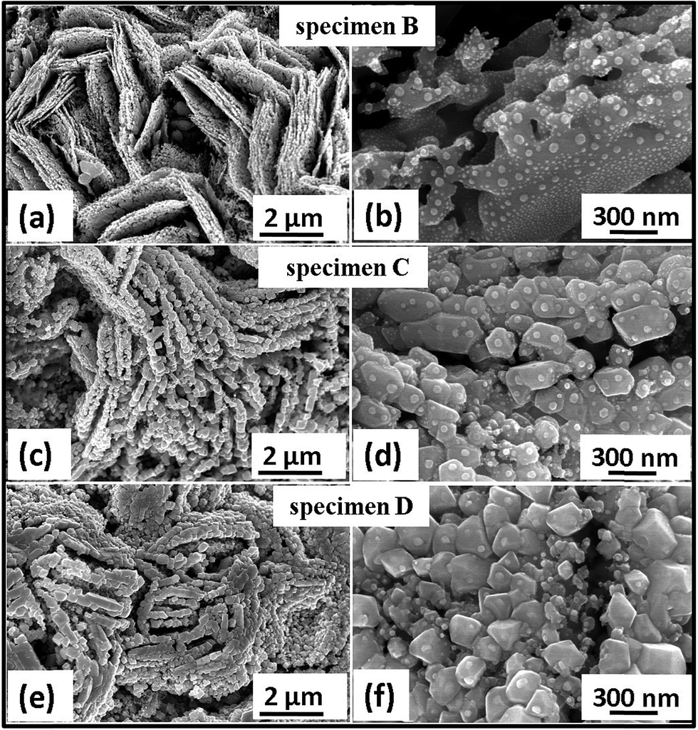 | ||
| Fig. 4 FESEM images of Au/CdO nanocomposite, (a) and (b) for specimen B (20 s Au coated CdO), (c) and (d) for specimen C (40 s Au coated CdO) and (e) and (f) for specimen D (60 s Au coated CdO). | ||
The specific surface area and pore size measurement is done by the Brunauer–Emmet–Teller (BET) method is found to be 3.9242 m2 g−1 and 9.1 nm respectively.
3.3. TEM analysis
The TEM characterizations of Au/CdO nanocomposite were carried out to reveal the crystallinity of synthesized product. Fig. 5(a) shows the bright field image of specimen B which clearly indicates uniform decoration of Au nanoparticles on the porous CdO nanosheets. Fig. 5(b) is the HRTEM image of specimen B, which depicts crystalline nature of porous CdO nanosheets with fringe spacing of 0.27 nm along (111) lattice plane. Also the fringe spacing of 0.24 nm has been seen for Au nanoparticles, which is consistent with literature value.32 Fig. 5(c) shows the SAED pattern of specimen B which indicates the polycrystalline nature of Au/CdO nanocomposite. | ||
| Fig. 5 TEM images of the Au/CdO nanocomposite (specimen B). (a) Low magnification bright field image, (b) HRTEM image of Au/CdO nanocomposite and (c) the corresponding selected area electron diffraction (SAED) pattern. | ||
3.4. Growth mechanism for porous aligned CdO nanosheets
The growth of porous aligned CdO nanosheets is due to dehydration. When as-synthesized Cd(OH)2 nanosheets are annealed at 450 °C, water vapour is released due to which the length of chemical bonds is changed from 0.231 nm (Cd–(OH)2) to 0.229 nm (Cd–O) which leads to contraction of the crystal lattice. So the tensile stress is formed on the surface and results in the cracking of the crystal lattice. Hence occurrence of the continuous breaking process finally leads to the formation of the porous CdO nanosheets. Detailed growth mechanism is shown schematically in Fig. 6. | ||
| Fig. 6 Growth mechanism of porous CdO nanosheets. | ||
3.5. Field emission studies
Fig. 7(a) depicts J–E plot of specimen A, B, C, and D. In present case, the current density J is defined as J = I/A, where I is the emission current and A is the overall area of the emitter (∼0.25 cm2). The applied field (E) is defined as E = V/d, where V is the applied voltage and d is the separation between anode and cathode. The values of the turn-on field, defined as the field required by material to draw an emission current density of 10 μA cm−2 for specimen A, B, C and D are found to be 1.9 V μm−1, 1.1 V μm−1, 2.4 V μm−1 and 2.8 V μm−1 respectively. Furthermore, the high current density of 530 μA cm−2 has been drawn from specimen A, B, C and D at an applied electric field of 2.9 V μm−1, 2.3V μm−1, 3.7 V μm−1 and 4.5 V μm−1 respectively. The observed field emission properties of all specimens A, B, C and D are listed in Table 1. The observed low turn-on field of specimen B is found to be superior than other semiconducting nanostructures reported in the Table 233–35 and also superior than the rest of all specimens. Zhao et al.33 synthesized the Si nanowires by chemical approach and decorate that by Au nanoparticles using thermal annealing in a hydrogen atmosphere and they found the turn-on field value at 1.9 V μm−1 for emission current density 10 μA cm−2. The ZnO nanopillars were synthesized by Chang et al.34 using simple vapor-phase transport process and Au nanoparticles decorated on ZnO nanopillars by sputter coater and they found the lowest turn of value at 2.65 V μm−1 for emission current density 10 μA cm−2. Also Chen et al.35 synthesized the boron nitride nanotubes by ball milling and annealing method and Au nanoparticles are decorated using dc sputtering, they found turn-on field value at 3.9 V μm−1 for emission current density 10 nA cm−2. | ||
| Fig. 7 (a) J–E plots of specimen A, B, C and D, indicating the exponential dependance (b) corresponding Fowler–Nordheim (F–N) plots. | ||
| Specimen | Turn-on field (V μm−1) (for 10 μA cm−2) | Maxm current density (530 μA cm−2) | Field enhancement factor (β) |
|---|---|---|---|
| A | 1.9 | 2.9 V μm−1 | 4302 |
| B | 1.1 | 2.3 V μm−1 | 5306 |
| C | 2.4 | 3.7 V μm−1 | 2110 |
| D | 2.8 | 4.5 V μm−1 | 1429 |
Observation of low turn-on field of specimen B is attributed to porous nature, high aspect ratio of nanosheets and nanometric dimension of Au nanoparticles which offers a large number of emission sites. As seen in FESEM images (Fig. 4(a and b)) the porous nanosheets are well covered by Au nanoparticles, which are responsible for creation of surface nanoprotrusions. These surface nanoprotrusions results into the increment in a local electric field. Schematic band diagram of Au/CdO nanocomposite is shown in Fig. 8. A large number of free electrons from CdO can move straight forward to the energy band or jump into the energy level of Au and further contribute for field emission.
 | ||
| Fig. 8 Energy band diagram of Au/CdO nanocomposite, indicating electron transport phenomenon across Au and CdO. | ||
The field emission behavior of specimen C and D is found to be not superior than specimen B. This is may be due to the thickness of Au film increases, the Au particle size is seen to be increases and also corresponding Au nanoparticles are decreases after annealing which is shown in Fig. 4(c–f).
The Fowler–Nordheim (F–N) plot, i.e., ln(J/E2) versus (1/E), derived from the observed J–E characteristic is shown in Fig. 7(b) which shows the non-linear behavior for all specimens (A–D). The emission current density obtained from an emitter depends exponentially on field enhancement factor (β), which is defined by the shape and size (i.e. aspect ratio) of the emitter.36 Field enhancement factor (β) has been calculated from the slope of the F–N plot using the following equation.37

By considering the work function of CdO as 3.45 eV (ref. 38) and for Au as 4.9 eV (ref. 39). The field enhancement factor (β) for all specimens A, B, C and D are calculated and found to be 4302, 5306, 2110 and 1429 respectively. The observed low turn-on field of specimen B may also attributed due to the high value of β.
Application point of view, the current stability is one of the important parameters for field emission study. The I–t plots for specimen A, B, C and D at the pre-set value of 1 μA recorded for a period of 3 h are depicted in Fig. 9. It is found that the emission current is nearly stable for all specimens. The appearance of ‘spike’ type fluctuations in the emission current is attributed to various atomic scale process such as desorption, adsorption, diffusion of residual gas species on the emitter surface.40 The average emission current remains constant for all specimens over the entire duration of measurement and shows no sign of degradation. Field emission images of all specimens are shown as an inset of Fig. 9. From the field emission images it is clear that a large number of tiny spots are observed for the specimen A, B and C. which indicating the participation of large emitters in field emission. However, in case of the specimen D small amount of tiny spots are observed. This may be due to the limited number of emitter sites.
 | ||
| Fig. 9 I–t plots at the preset value of 1 μA for specimen A, B, C and D. The inset shows a typical field emission images which are indicating large number of tiny spots. | ||
4. Conclusions
Simple and economic route of thermal annealing was employed for the Au nanoparticles decoration on porous CdO nanosheets. Decoration of the porous CdO nanosheets by Au nanoparticles with an average diameter of 15 nm (specimen B) leads to superior field emission characteristics, with a low turn-on field value of 1.1 V μm−1 for emission current density 10 μA cm−2. Quite inexpensive route of synthesis of Au/CdO nanocomposite with excellent field emission results, indicates the possible applicability of the present emitter in micro/nano electronic devices.Acknowledgements
GPP and PGC sincerely thank to DST SERB (Ref. No. SB/EMEQ-208/2013 dated 23/08/2013) for financial support.References
- W. Bai, X. Zhu, Z. Zhu and J. Chu, Appl. Surf. Sci., 2008, 224, 6483–6488 CrossRef.
- R. W. Siegel, Physics of New Materials, ed. F. E. Fujita, Springer-Verlag Berlin, Geidelberg, ch. 4, 1994 Search PubMed.
- R. P. Andre, Mater. Res., 1989, 4, 704–736 CrossRef.
- H. Z. Gleiter, Metallkd., 1995, 86, 78–83 CAS.
- K. Dewangan, G. P. Patil, R. V. Kashid, V. S. Bagal, M. A. More, D. S. Joag, N. S. Gajbhiye and P. G. Chavan, Vacuum, 2014, 109, 223–229 CrossRef CAS.
- Y. Wang, J. Cao, S. Wang, X. Guo, J. Zhang, H. Xia, S. Zhang and S. Wu, J. Phys. Chem. C, 2008, 112, 17804–17808 CAS.
- J. Liu, Z. Guo, F. Meng, T. Luo, M. Li and J. Liu, Nanotechnology, 2009, 20, 125501 CrossRef PubMed.
- N. Shanmugam, B. Saravanan, R. Reagan, N. Kannadasan, K. Sathishkumar and S. Cholan, Mod. Chem. Appl., 2014, 2, 1000124 Search PubMed.
- Z. X. Yang, W. Zhong, Y. X. Yin, X. Du, Y. Deng, C. Au and Y. W. Du, Nanoscale Res. Lett., 2010, 5, 961–965 CrossRef CAS PubMed.
- R. Ferro and I. A. Rodriguez, Sol. Energy Mater. Sol. Cells, 2000, 64, 363–370 CrossRef CAS.
- M. Ristic, S. Poporic and S. Music, Mater. Lett., 2004, 58, 2494–2499 CrossRef CAS.
- T. K. Subramanyam, S. Uthanna and N. B. Srinivasulu, Mater. Lett., 1998, 35, 214–220 CrossRef CAS.
- A. K. Srivastava, S. Pandey, K. N. Sood, S. K. Halder and R. Kishore, Mater. Lett., 2008, 62, 727–730 CrossRef CAS.
- X. Wu, R. Wang, B. Zou, P. Wu, L. Wang, J. Xu and W. Huang, Appl. Phys. Lett., 1997, 71, 2097–2099 CrossRef CAS.
- X. Liu, C. Li, S. Han, J. Han and C. Jhou, Appl. Phys. Lett., 2003, 82, 1950–1952 CrossRef CAS.
- Y. H. Luo, J. Huang and I. Ichinose, J. Am. Chem. Soc., 2005, 127, 8296–8297 CrossRef CAS PubMed.
- I. Paramasivam, J. M. Macak and P. Schmuki, Electrochem. Commun., 2008, 10, 71–75 CrossRef CAS.
- X. He, Y. Cai, H. Zhang and C. Liang, J. Mater. Chem., 2011, 21, 475–480 RSC.
- C. Ye, Y. Bando, X. Fang, G. Shen and D. Golberg, J. Phys. Chem. C, 2007, 111, 12673–12676 CAS.
- F. J. Sheini, J. Singh, O. N. Srivasatva, D. S. Joag and M. A. More, Appl. Surf. Sci., 2010, 256, 2110–2214 CrossRef.
- M. C. Daniel and D. Astruc, Chem. Rev., 2004, 104, 293–346 CrossRef CAS PubMed.
- F. Li, L. Zhang, S. Wu, Z. Li, Y. Wang and X. Liu, Mater. Lett., 2015, 145, 209–211 CrossRef CAS.
- F. Li, S. Wu, L. Zhang and Z. Li, Appl. Phys. A: Mater. Sci. Process., 2015, 120, 1383–1389 CrossRef CAS.
- P. G. Chavan, S. S. Badadhe, I. S. Mulla, M. A. More and D. S. Joag, Nanoscale, 2011, 3, 1078–1083 RSC.
- D. J. Late, M. A. More, S. Sinha, K. Dasgupta, P. Mishra and B. N. Singh, et al., Appl. Phys. A: Mater. Sci. Process., 2011, 104, 677 CrossRef CAS.
- G. Hodes, Chemical Solution Deposition of Semiconductor films, Marcel Dekker, Inc., New York, 2002, p. 7 Search PubMed.
- D. S. Dhawale, A. M. More, S. S. Latthe, K. Y. Rajpure and C. D. Lokhande, Appl. Surf. Sci., 2008, 254, 3269–3273 CrossRef CAS.
- S. K. Panda, A. Datta, G. Sinha, S. Chaudhuri, P. G. Chavan, S. S. Patil, M. A. More and D. S. Joag, J. Phys. Chem. C, 2008, 112, 6240–6244 CAS.
- Z. Y. Zou, Q. Wang, X. J. Chen and S. L. Qu, J. Appl. Phys., 2009, 105, 103114 CrossRef.
- G. A. Rance, D. H. Marsh, S. J. Bourne, T. J. Reade and A. N. Khlobystov, ACS Nano, 2010, 4(8), 4920–4928 CrossRef CAS PubMed.
- H. Kim, C. Choi, J. Khamwannah, S. Y. Noh, Y. Zhang, T. Y. Seong and S. Jin, J. Renewable Sustainable Energy, 2013, 5, 053104 CrossRef.
- Z. X. Yang, W. Zhong, Y. X. Yin, X. Du, Y. Deng, C. Au and Y. W. Du, Nanoscale Res. Lett., 2010, 5, 961–965 CrossRef CAS PubMed.
- F. Zhao, G. Cheng, R. Zheng, D. Zhao, S. Wu and J. Deng, Nanoscale Res. Lett., 2011, 6, 176 CrossRef PubMed.
- Y. M. Chang, M. L. Lin, T. Y. Lai, H. Y. Lee, C. M. Lin, Y. C. Wu and J. Y. Juang, ACS Appl. Mater. Interfaces, 2012, 4, 6676–6682 CAS.
- H. Chen, H. Zhang, L. Fu, Y. Chen, J. S. Williams, C. Yu and D. Yu, Appl. Phys. Lett., 2008, 92, 243105 CrossRef.
- G. P. Patil, V. S. Bagal, C. R. Mahajan, V. R. Chaudhari, S. R. Suryawanshi, M. A. More and P. G. Chavan, Vacuum, 2016, 123, 167–174 CrossRef CAS.
- S. R. Suryawanshi, A. K. Singh, M. Deo, D. J. Late, S. Sinha and M. A. More, CrystEngComm, 2015, 17(21), 3936–3944 RSC.
- D. Xi, Nanostructured Conjugated Polymers for Photovoltaic Devices, University of California, Los Angeles, 2008, p. 76 Search PubMed.
- S. Wang, Fundamentals of Semiconductor Theory and Device Physics, Prentice-Hall Inc., NJ, 1989, p. 131 Search PubMed.
- G. Sinha, S. K. Panda, A. Datta, P. G. Chavan, D. R. Shinde, M. A. More, D. S. Joag and A. Patra, ACS Appl. Mater. Interfaces, 2011, 3, 2130 CAS.
Footnote |
| † Electronic supplementary information (ESI) available. See DOI: 10.1039/c5ra28000a |
| This journal is © The Royal Society of Chemistry 2016 |