Highly sensitive electrochemical detection of circulating tumor DNA based on thin-layer MoS2/graphene composites

Yilan Chu, Bin Cai, Ye Ma, Minggang Zhao, Zhizhen Ye* and Jingyun Huang*
School of Materials Science and Engineering, Zhejiang University of China, Hangzhou, 310027, China. E-mail: huangjy@zju.edu.cn; yezz@zju.edu.cn

Received 24th December 2015 , Accepted 4th February 2016

First published on 12th February 2016


Abstract

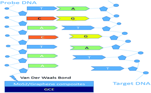
By integrating thin-layer molybdenum disulfide (MoS2) and graphene through a hydrothermal process and an ultrasonic method, a label-free, amplification-free and ultrasensitive circulating tumor DNA electrochemical sensor was made. Compared with other methods, this preparation process was simpler and the electrochemical properties were enhanced. Using a differential pulse voltammetry test, this sensor can detect trace amounts of DNA in the range from 10−16 M to 10−13 M. Compared with other methods that are used to detect the same circulating tumor DNA, this sensor has an obvious advantage in sensitivity, cost and simplicity because it removes the need for labelling processes and amplifiers.


1. Introduction

Thin-layer molybdenum disulfide (MoS2) is a new material that has the properties of a two-dimensional (2-D) material. In thin 2-D materials free charges are immobile in one spatial dimension, but mobile in the other two. This property enables 2-D materials to have new or superior functions, distinct from traditional bulk materials or thin films.1 And its outstanding properties like direct semiconducting gap, excellent optical properties and great mechanical properties make it a promising material in photovoltaics, nanoelectronics, energy storage, catalysis and biosensing.2

Nowadays gene diagnosis and therapy attract more and more attention because of its application in many aspects such as tumor detection, forensic investigation and environmental monitoring.3–6 Among the methods for gene detection, the electrochemical DNA sensor aiming at the detection of oligonucleotide sequences is a promising and convenient way to detect specific gene sequences, especially at low physiological levels. There are some other methods based on optical and chemiluminescence properties that have been widely used in the modern life. However, these methods usually have some shortcomings. For example, the chemiluminescence DNA biosensor needs to label the oligonucleotide probes that increases the cost and complexity. Compared with these methods, electrochemical DNA biosensor is label-free and enzyme-free which provides convenience. The complexity is reduced and the test time could be greatly shortened.7–9 Because of these merits, electrochemical biosensors have received more attention and been applied widely in DNA detection.

In DNA detection, circulating tumor DNA (ctDNA) detection is a new and prospering application direction because of its value in tumor prognosis and treatment.10 Circulating tumor DNA could be used as a biomarker. It is a double stranded DNA which has tumor-specific sequence mutations and its existence could be a proof of specific cancer. ctDNA could be found in the cell-free fraction of blood which means the detection just need a sample of blood instead of tissue biopsy. This feature could reduce the risk of patients and provide convenience. The traditional biopsy which is widely used for cancer prognostic procedure is inadequate according to the result made by Charles Swanton. The result shows that biopsy may miss mutations away in a small range that might affect the judgment of illness.11 Besides, the information provided by biopsies is static and could not reflect real-time dynamic of the tumor. On the contrary, the ctDNA detection can monitor the evolution and offer more comprehensive data of tumor. It can help doctors know about therapeutic effect of present treatment and resistance evolution.12 However, concentrations of ctDNA is quite low and hard to detect. The amounts of ctDNA are typically low and extremely variable. Usually ctDNA makes up barely 1–0.01% of the circulating DNA in blood. When people have very advanced cancers, the ctDNA come from tumors and the concentration would increase. For this reason, early sequencing technologies were unable to detect the ctDNA and the sensitivity of the ctDNA sensor is very important.12

In order to improve detection limit, many efforts have been made, such as surface plasmon resonance (SPR) biosensors.10,13,14 In 2014, Huang et al. combine MoS2 with multi-walled carbon nanotubes to improve the electronic conductivity and electrochemical activity, then the composites were further combined with gold nanoparticles to immobilize DNA on the composites' surface via Au–S bonds self-assembly. By enzyme multiple signal amplification, the DNA biosensor could achieve sub-femtomolar DNA detection, that would improve the limit of detection.

In this contribution, an ultra-sensitive label-free electrochemical biosensor for detecting ctDNA was made. To improve the electronic conductivity and electrochemical activity, MoS2 was integrated with graphene by hydrothermal method, which was further ultrasonicated for 6 h to get the MoS2/graphene nanosheets, and probe DNA could be directly immobilized on the nanosheets by van der Waals force between nucleobases of single stranded DNA (ssDNA) and the basal plane of nano MoS2.16 Then K3[Fe(CN)6] was used as the electroactive indicator to monitor the changes happened on the electrode surface. The changes caused by DNA immobilization and hybridization were detected by directly monitoring the differential pulse voltammetric (DPV) response of the guanine bases. Compared with other biosensors, such a sensor is quite convenient and cheap because there is no fluorophore labelling and enzyme amplification step. In addition, the high sensitivity is also a remarkable advantage.10

2. Experimental section

2.1. Reagents and instruments

Electrochemical measurements were performed on a CHI 760E electrochemical workstation (Shanghai CH Instrument Company, China) with a conventional three-electrode system. A platinum wire was used as the auxiliary electrode, a saturated calomel as the reference electrode (SCE) and the MoS2/graphene composites modified GCE as the working electrode. The composites were characterized by scanning electron microscopy (SEM, FB2200/S3400N machine, HIT, Tokyo, Japan) and transmission electron microscopy (TEM, Titan ChemiSTEM, FEI, USA). X-ray diffraction (XRD) pattern was obtained on Bede D1 X-ray diffraction system. Raman spectra was obtained on a Raman system model 1000 spectrometer at room temperature. Brunauer–Emmett–Teller (BET) tests were made on surface area analyzer (Autosorb-1-C).

Graphene oxide suspension (2 mg mL−1, dissolved in deionized water) was purchased from Tanmei Sinocarbon Materials Technology Company (Taiyuan, China). The bulk MoS2, L-cysteine, NaOH, KCl, K3[Fe(CN)6], N,N-dimethylformamide (DMF) and Na2MoO4·2H2O were purchased from Tianjin Ba Si Fu Reagent Company (Tianjin, China).

The DNA oligonucleotides were synthesized by Shanghai Sangon Biological Engineering Technological Co. Ltd (Shanghai, China). Their base sequences are listed below:

Probe DNA (pDNA): 5′-AGT GAT TTT AGA GAG-3′;

Complementary DNA (cDNA): 5′-TCA CTA AAA TCT CTC-3′;

One-mid-base mismatch ssDNA (1MTDNA): 5′-TCA CTA ATA TCT CT-3′;

Two-mid-bases mismatch ssDNA (2MTDNA): 5′-TCA CAA ATA TCT CT-3′;

Non-complementary ssDNA (ncDNA): 5′-CAC TCC GCG CTA ACT-3′.

2.2. Preparation of MoS2/graphene composites modified GCE

Fig. 1 is the electrode setup for DNA detection. The MoS2/graphene composites were prepared as follows: 39.7 mL graphene oxide suspension was diluted in 40 mL deionized water. Then 0.3 g Na2MoO4·2H2O was added into the suspension. After 20 minutes stirring, the pH value of the mixture was adjusted to 6.5 with 0.1 M NaOH and then 0.8 g L-cysteine was added into the mixture. After vigorous stirring for about 1 h, the mixture was transferred into a 100 mL Teflon-lined stainless steel autoclave and heated at 180 °C for 24 h.
image file: c5ra27625j-f1.tif
Fig. 1 Electrode setup figure for DNA detection.

Then transfer the residue into 100 mL deionized water, stir the mixture for about 1 h and followed by ultrasonication for 6 h and get a homogenous suspension of nano MoS2/graphene composites (0.01 M). The GCE was sequentially polished with 0.3 and 0.05 μm alumina slurries and rinsed with acetone, 0.5 M water dilute nitric acid for 1 min, respectively. Drip 40.0 μL of the suspension on the polished GCE surface and dried naturally at room temperature. Then the composites modified GCE was prepared. For comparison, the same concentration of MoS2 homogenous suspension was also prepared and tested.

2.3. Immobilization and hybridization of DNA

As 57 °C is the recommended hybridization temperature in the oligo product information offered by the Shanghai Sangon Biological Engineering Technological company, 20.0 μL probe DNA (pDNA) solution (pH 7.0, containing 1.0 × 10⁻⁶ M pDNA) was dripped on the nano MoS2/graphene modified GCE surface and dried in a drying oven at 57 °C for 35 min. After pDNA immobilization, dripping 20.0 μL complementary DNA (cDNA) on the pDNA modified GCE surface and similarly dried in the drying oven at 57 °C for 30 min to hybridize the pDNA and the cDNA. Then keep the electrode in 1.0 M KCl solution containing 0.2 M K3[Fe(CN)6] at −0.7 V for 300 s to release the double-stranded DNA (dsDNA) which is produced by hybridization of pDNA and cDNA.7,17,18 After rinsing with deionized water the electrode started electrochemical measurements.

2.4. Electrochemical measurements

Cyclic voltammetry (CV) experiments were recorded in 1.0 M KCl solution containing 0.2 M K3[Fe(CN)6] at a scan rate of 0.10 V s−1 from 0.6 V to −0.3 V. It cost 1 min. Electrochemical impedance spectroscopy (EIS) experiment was also made in the 1.0 M KCl solution containing 0.2 M K3[Fe(CN)6]. The ac voltage amplitude was 5 mV, and the voltage frequencies were ranged from 105 Hz to 0.01 Hz. The applied potential was 0.281 V (vs. GCE). It cost about 15 min. Differential pulse voltammetry (DPV) experiments were recorded in the same solution at a pulse amplitude of 0.05 V, a pulse width of 0.05 s, and a pulse period of 0.5 s. Before DPV scanning the electrode underwent a process of preconditioning at −0.7 V for 300 s with gentle agitation and quiet for 2 s. All experiments were carried out at room temperature.

3. Results and discussion

3.1. Characterization of MoS2/graphene composites

The MoS2/graphene composites were prepared by a method which combined the hydrothermal method and the ultrasound exfoliation method. The SEM images which are listed below showed the surface morphology of the composites which had not been ultrasound exfoliated. Fig. 2A is the SEM image of the MoS2/graphene (1[thin space (1/6-em)]:[thin space (1/6-em)]1) composites and it shows that the composites have sphere-like morphology consisting of nano MoS2 sheets and graphene forms a 3D architecture which combines MoS2 sphere-like structures. Fig. 2B is the SEM image of the MoS2/graphene (1[thin space (1/6-em)]:[thin space (1/6-em)]2) composites and it shows a plate-like morphology implying a smaller specific surface area that is not good for biosensing performance. Fig. 2C is the SEM image of the MoS2/graphene (2[thin space (1/6-em)]:[thin space (1/6-em)]1) composites and it shows a same plate morphology like MoS2/graphene (1[thin space (1/6-em)]:[thin space (1/6-em)]2) composites.
image file: c5ra27625j-f2.tif
Fig. 2 Morphology (A) SEM images of MoS2/graphene (1[thin space (1/6-em)]:[thin space (1/6-em)]1) composites. (B) MoS2/graphene (2[thin space (1/6-em)]:[thin space (1/6-em)]1) composites. (C) MoS2/graphene (1[thin space (1/6-em)]:[thin space (1/6-em)]2) composites.

Fig. 3A is the XRD patterns of the MoS2/graphene (1[thin space (1/6-em)]:[thin space (1/6-em)]1) composite and pure MoS2. From the pattern we can see that diffraction peaks of the MoS2/graphene composite show at 2θ = 15°, 33°, 40° and 59°, which corresponds to (002), (100), (103), and (110) planes of MoS2 (JCPDS no. 37-1492), respectively.19 The pattern of MoS2/graphene composites is similar with the pattern of pure MoS2 material. One reason of this phenomenon is that graphene usually does not have obvious and particular peak in XRD pattern. And all the peak widths are wide, which shows that the composites have poorly crystalline due to amorphism of the composites. The amorphism of the composites was attributed to the hydrothermal process used to incorporate the MoS2 nanosheets and graphene. Because the graphene inhibited the growth of the layered MoS2 crystalin the hydrothermal process.15


image file: c5ra27625j-f3.tif
Fig. 3 (A) XRD patterns of MoS2 nanosheets and MoS2/graphene (1[thin space (1/6-em)]:[thin space (1/6-em)]1) composites. (B) Raman spectra of MoS2/graphene (1[thin space (1/6-em)]:[thin space (1/6-em)]1) composites.

For further confirming the prepared material and the structural and electronic properties, the Raman spectrum of the MoS2/graphene composites was recorded (Fig. 3B). The Raman spectrum showed two strong bands at 1342 cm−1 that was caused by sp3-hybridized carbon and the G bands at 1586 cm−1 that was because of the E2g zone center mode of the graphene. And the other bands at 357.3 cm−1 and 409.2 cm−1 were the characteristic bands of MoS2 which aroused from the E2g and A1g peaks respectively.20 Above-mentioned peaks could prove the presence of graphene and MoS2 in the composites, which was consistent with the results in the XRD diffraction studies.

Fig. 4 is the TEM image of the MoS2/graphene (1[thin space (1/6-em)]:[thin space (1/6-em)]1) composites which were ultrasound exfoliated for 6 h. From the Fig. 4A, we can see that the composites are thin sheets morphologies and have large specific surface area which were in agreement with the SEM images. The images showed the composites had thin layer structure and the layers folded and tangled together. From Fig. 4B, graphene inserted in the layered MoS2 nanosheets and the MoS2 served as the substrate. This was because in the preparation process, MoS2 sheets served as the substrate for the nucleation and growth of graphene and turned to a layered structure. The presence of the graphene disturbed the growth of the layered structure, and the 6 h exfoliation promoted the separation of the layered structure of the composites, too. These factors directly influence the structure of the composites, which turned the material to the few-layer MoS2/graphene composites. Such a thin-layer structure remarkably increased the specific surface area and the recombination of the MoS2 and the graphene enhanced the electrical conductivity, which promoted the upgrade of the electrochemical performances of the MoS2/graphene composites. Also the BET tests showed that the specific surface area of 2D MoS2/graphene composites is 12.42 m2 g−1 and the specific surface area of bulk MoS2 is 3.62 m2 g−1, that proved this analysis.


image file: c5ra27625j-f4.tif
Fig. 4 (A and B) TEM images of MoS2/graphene (1[thin space (1/6-em)]:[thin space (1/6-em)]1) composites. (C) TEM images of graphene. (D) TEM images of MoS2.

Fig. 5 is the TEM surface scanning spectrum diagram scanned by energy dispersive spectrometer (EDS). Fig. 5A displays the K-spectrum of the carbon, Fig. 5B displays the K-spectrum of the molybdenum and Fig. 5C displays the K-spectrum of the sulfide. These figures display the distribution of three elements in the same area. The bright areas of the spectra are almost the same and coincident, which shows that the graphene and MoS2 were relatively well distributed in the composites nanosheets.


image file: c5ra27625j-f5.tif
Fig. 5 EDS images of MoS2/graphene (1[thin space (1/6-em)]:[thin space (1/6-em)]1) composites. (A) K-spectrum of C. (B) K-spectrum of Mo. (C) K-spectrum of S.

3.2. Electrochemical characterization of MoS2/graphene composites

3.2.1 CV response of different electrodes. The cyclic voltammetry (CV) was performed in a 1.0 M KCl solution containing 0.2 M K3[Fe(CN)6] solution and was used to characterize the modification of the GCE and the DNA fixation on the modified GCE. Fig. 6A shows the CV curves of bare GCE, MoS2/graphene composites modified GCE, 100 μM probe DNA immobilized MoS2/graphene/GCE, another bare GCE, bulk MoS2 modified GCE and 100 μM probe DNA immobilized bulk MoS2/GCE. The MoS2/graphene composites modified GCE showed higher redox peak currents and a little wider ΔEp (the difference of peak potentials) than bare GCE.
image file: c5ra27625j-f6.tif
Fig. 6 (A) CVs of different electrodes (GCE 1, MoS2/graphene (1[thin space (1/6-em)]:[thin space (1/6-em)]1) composites modified GCE 1, pDNA immobilized MoS2/graphene (1[thin space (1/6-em)]:[thin space (1/6-em)]1) composites modified GCE 1, GCE 2, bulk MoS2/GCE 2, pDNA immobilized MoS2/GCE 2) in a 1.0 M KCl solution containing 0.2 M K3[Fe(CN)6] solution. (B) Nyquist diagrams of different electrodes in a 1.0 M KCl solution containing 0.1 M K3[Fe(CN)6] solution. The red spots are bulk MoS2/GCE and the black spots are MoS2/graphene (1[thin space (1/6-em)]:[thin space (1/6-em)]1) composites modified GCE.

As the concentration of the electrolyte was the same, the higher peak current confirmed that the composites modified GCE had good electrochemical activity. The CV curve of the pDNA modified GCE showed significantly difference with the other two curves as the pDNA adsorbed on the electrode surface and changed its electrical conductivity. The figure showed that the anodic peak current value of the probe DNA immobilized MoS2/graphene composites modified GCE had an obvious increase compared with the probe DNA immobilized bulk MoS2 modified GCE, while the peak current of the composites modified GCE was quite close with the bulk MoS2 modified GCE.

From the formula ‘i = FAC*0(D0b)1/2π1/2χ(σb)’. The current is directly proportional to C0 (initial concentration of reactants) and ν1/2 (scanning speed). The scanning speed is fixed and the initial concentration of reactants is proportional to the weight of reactants. So the weight of reactants (MoS2) is involved in the decrease/increase in conductivity. As the pure bulk MoS2 material weighed more, this phenomenon showed that the nano MoS2/graphene composites had better electrical conductivity than the bulk MoS2 material which meant that compounded with graphene improved the conductivity of the nano MoS2 material. The decrease of the probe DNA immobilized bulk MoS2 modified GCE showed that bulk MoS2 could not effectively adsorbed probe DNA which means that the electrode cannot gather K3[Fe(CN)6] because of its poor specific surface area. And graphene and similar 2D structure materials have nucleobase–graphene inter-molecular π–π stacking interactions with ssDNA, that is also beneficial to immobilize ssDNA on the 2D MoS2/graphene composites.21 And this phenomenon also proved that the probe DNA has been immobilized on the nano MoS2/graphene composites modified electrode surface.

3.2.2 EIS response of different electrodes. The electrochemical impedance spectroscopy experiment (EIS) was made in the 1.0 M KCl solution containing 0.2 M K3[Fe(CN)6]. The EIS results also proved that the nano MoS2/graphene composites had better electrical conductivity than the bulk MoS2 material.

Fig. 6B is the Nyquist diagram of nano MoS2/graphene modified GCE and bulk MoS2 modified GCE. The interface electron-transfer resistance (Ret) was the diameter of arc in the high-frequency section of the curve and the figure displays composites had lower Ret than the bulk MoS2 owing to the better electric conductivity. Ret (composites) = 172 ohm, Ret (MoS2) = 225.5 ohm. The EIS experiments were in good accordance with the DPV experiments presented later on.

3.2.3 Working mechanism of the sensor. The usual DNA monitor is EB in the past experiments. As K3[Fe(CN)6] could monitor the change of the electrode surface which was induced by the hybridization of the probe DNA and complementary DNA while ethidium bromide (EB) has certain carcinogenic risk, here we used K3[Fe(CN)6] to replace EB as the electroactive indicator. The DPV curves comparison was shown in the Fig. 7.
image file: c5ra27625j-f7.tif
Fig. 7 DPV plots of K3[Fe(CN)6] at pDNA immobilized MoS2/graphene composites modified GCE before and after immobilization.

The DPV plots (Fig. 7) showed the signals of K3[Fe(CN)6] at probe DNA immobilized MoS2/graphene composites modified GCE before and after pDNA immobilization. From the plots we can see that after the pDNA immobilized on the modified GCE, the DPV anodic peak current value had an increase and it was caused by more [Fe(CN)6]3− gathering together around the probe DNA immobilized electrode surface. From this we can know that probe DNA had been successfully bounded to the MoS2/graphene composites modified GCE surface. Xinxing Wang and his team had made a work proving that the positively charged guanine and adenine could not only adsorb on the nano MoS2 surface via the van der Waals force, but also through electrostatic adsorption.7 Before this experiment, another probe DNA (5′-CGA CAG TGG TCC CAA AGA-3′) which had been used and in that experiment the concentration of the K3[Fe(CN)6] was one half of this experiment while the oxidation peak current value of DPV signals was the same. Comparing two probe DNA, the biggest difference was the base number (5′-AGT GAT TTT AGA GAG-3′ and 5′-CGA CAG TGG TCC CAA AGA-3′). It also implied that the MoS2/graphene composites could immobilize the probe DNA because of the van der Waals bond between the probe DNA and the nanosheets.

3.2.4 DPV results analysis. In this experiment, we use the synthetic sequence of the E542K oligonucleotide probe of the PIK3CA gene related to gastric carcinoma as the target DNA to investigate the specific complementary ssDNA on the nano MoS2/graphene sensing platform.

Fig. 8A shows the DPV signals of the nano MoS2/graphene composites modified GCE after different concentration (1.0 × 10⁻¹⁷ M to 1.0 × 10⁻¹² M, 20 μL) cDNA hybridizing with the pDNA and probe DNA immobilized MoS2/graphene composites modified GCE. The DPV experiment was made in the 1.0 M KCl solution containing 0.2 M K3[Fe(CN)6]. We can see that the DPV signal of oxidation peak current value had an obvious decrease which illustrates that the amount of remaining pDNA had decreased, because the dsDNA formed by the hybridization of pDNA and cDNA had been released from the electrode surface by the electrochemical pretreatment (−0.7 V, 300 s). From the change of the DPV signals we can see that with the hybridization the oxidation peak current value decreased fast. It shows an opposite tend with that in pDNA immobilization, which proves that the amount of pDNA has decreased and the hybridization has successfully conducted.


image file: c5ra27625j-f8.tif
Fig. 8 (A) DPV plots of 0.2 M K3[Fe(CN)6] at pDNA (1.0 × 10⁻⁶ M) immobilized MoS2/graphene composites modified GCE in 1.0 M KCl and that after hybridization with different concentrations of E542K gene sequence. (B) The plot of −ΔIpc vs. the logarithm of E542K gene sequence concentrations.

From the DPV plots we can find that with the hybridization conducting the oxidation peak current value decreases, and the difference (namely ΔIpc) between the oxidation peak current value of K3[Fe(CN)6] could be used as the measurement signal. As the plot of 10−12 M and 10−17 M deflected too much, the linear relationship used the data from 10−16 M to 10−13 M. And from the data we can conclude a linear relationship between ΔIpc and the concentration of the target (cDNA) from 1.0 × 10⁻¹⁶ M to 1.0 × 10⁻¹³ M, and the R square is 0.985, the regression equation is −ΔIpc/A = 1.142[thin space (1/6-em)]log[thin space (1/6-em)]C/M − 22.761. The limit of detection (LOD) is 10−17 M and 10−12 M is the value at which the response starts reaching a plateau. Fig. 8B is figure of the linear fit. And this detection limit is the remarkable sub-femtomolar LOD of our assay compares well with that of similar magnitude previously reported by other with the same E542K gene detection (50 fM) and similar gene detection (miRNA-21, 100 aM).10,22 These results show that the nano MoS2/graphene composites modified GCE has high electrochemical activity and has an ultrahigh sensitivity for the DNA biosensing.

Fig. 9 compares three percentages of ΔIpc/Ipc in different ssDNA hybridization with the probe DNA including one-middle-base mismatched DNA (1MT DNA), two-middle-bases-mismatched DNA (2MT DNA) and non-complementary DNA (ncDNA) sequence.


image file: c5ra27625j-f9.tif
Fig. 9 Comparison of hybridization signal changes for pDNA immobilized MoS2/graphene composites modified GCE with cDNA, single-base mismatched DNA (1MT DNA), three-base mismatched DNA (3MT DNA), and non-complementary DNA (ncDNA). The detection concentrations of these sequences were all selected as 1.0 × 10⁻¹⁷ M.

From the figure we can see that the highest ΔIpc is the complementary DNA sequence followed by 1MT DNA, 2MT DNA and the non-complementary DNA successively. Compared with the ΔIpc of the complementary DNA, the signal decrease of the non-complementary DNA was much lower and could be neglected. Although the selectivity of 1MT DNA is not so good, other mismatched DNA sequences can be easily distinguished. From this result we can conclude that the specificity of the DNA sensor is high selectivity and could distinguish most mismatched DNA sequences.

3.2.5 High sensitivity explanation. As MoS2/graphene composites have large specific surface area, the amount of fixed pDNA can be increased. This property is beneficial to the fixation of ssDNA on the composites and it improves the sensitivity. The nucleobase–graphene inter-molecular π–π stacking interactions also help immobilize ssDNA on the 2D MoS2/graphene composites modified GCE. Besides the combination of graphene and MoS2 improves the electric conductivity of the composites, that also enhance the sensitivity.

4. Conclusions

Here a new ultra-sensitive and selective label-free electrochemical circulating tumor DNA sensing platform based on the prepared nano MoS2/graphene composites has been developed. The material was made by simply integrating nano MoS2 and graphene through hydrothermal process and ultrasonic method. As the sensor avoided the dye labelling and enzyme amplifying process, the cost and simplicity of the sensor preparation is largely decreased. The limit of detection could get 1 × 10⁻¹⁷ M and detection range is from the 1.0 × 10⁻¹⁶ M to 1.0 × 10⁻¹³ M. Also the proposed sensor could be used in detecting other probe DNA.

Acknowledgements

This work was financially supported by National Natural Science Foundation of China (91333203), Natural Science Foundation of Zhejiang province (LY14E020006).

Notes and references

  1. S. Das, M. Kim, J. W. Lee and W. Choi, Crit. Rev. Solid State Mater. Sci., 2014, 39, 231–252 CrossRef CAS.
  2. S. Z. Butler, S. M. Hollen, L. Y. Cao, Y. Cui, J. A. Gupta, H. R. Gutierrez, T. F. Heinz, S. S. Hong, J. X. Huang, A. F. Ismach, E. Johnston-Halperin, M. Kuno, V. V. Plashnitsa, R. D. Robinson, R. S. Ruoff, S. Salahuddin, J. Shan, L. Shi, M. G. Spencer, M. Terrones, W. Windl and J. E. Goldberger, ACS Nano, 2013, 7, 2898–2926 CrossRef CAS PubMed.
  3. H. F. Cui, L. Cheng, J. Zhang, R. H. Liu, C. Zhang and H. Fan, Biosens. Bioelectron., 2014, 56, 124–128 CrossRef CAS PubMed.
  4. S. Jampasa, W. Wonsawat, N. Rodthongkum, W. Siangproh, P. Yanatatsaneejit, T. Vilaivan and O. Chailapakul, Biosens. Bioelectron., 2014, 54, 428–434 CrossRef CAS PubMed.
  5. J. Sui, L. J. Zhang and H. Peng, Eur. Polym. J., 2013, 49, 139–146 CrossRef CAS.
  6. S. Y. Niu, J. Sun, C. C. Nan and J. H. Lin, Sens. Actuators, B, 2013, 176, 58–63 CrossRef CAS.
  7. X. Wang, F. Nan, J. Zhao, T. Yang, T. Ge and K. Jiao, Biosens. Bioelectron., 2015, 64, 386–391 CrossRef CAS PubMed.
  8. Y. Wan, H. Xu, Y. Su, X. H. Zhu, S. P. Song and C. H. Fan, Biosens. Bioelectron., 2013, 41, 526–531 CrossRef CAS PubMed.
  9. W. Yao, L. Wang, H. Y. Wang, X. L. Zhang, L. Li, N. Zhang, L. Pan and N. N. Xing, Biosens. Bioelectron., 2013, 40, 356–361 CrossRef CAS PubMed.
  10. A. H. Nguyen and S. J. Sim, Biosens. Bioelectron., 2015, 67, 443–449 CrossRef CAS PubMed.
  11. M. Gerlinger, A. J. Rowan, S. Horswell, J. Larkin, D. Endesfelder, E. Gronroos, P. Martinez, N. Matthews, A. Stewart, P. Tarpey, I. Varela, B. Phillimore, S. Begum, N. Q. McDonald, A. Butler, D. Jones, K. Raine, C. Latimer, C. R. Santos, M. Nohadani, A. C. Eklund, B. Spencer-Dene, G. Clark, L. Pickering, G. Stamp, M. Gore, Z. Szallasi, J. Downward, P. A. Futreal and C. Swanton, N. Engl. J. Med., 2012, 366, 883–892 CrossRef CAS PubMed.
  12. E. Yong, Nature, 2014, 511, 524–526 CrossRef CAS PubMed.
  13. K. E. Fong and L. Y. L. Yung, Nanoscale, 2013, 5, 12043–12071 RSC.
  14. K. A. Willets and R. P. Van Duyne, in Annual Review Of Physical Chemistry, Annual Reviews, Palo Alto, 2007, vol. 58, pp. 267–297 Search PubMed.
  15. K. J. Huang, Y. J. Liu, H. B. Wang, Y. Y. Wang and Y. M. Liu, Biosens. Bioelectron., 2014, 55, 195–202 CrossRef CAS PubMed.
  16. C. F. Zhu, Z. Y. Zeng, H. Li, F. Li, C. H. Fan and H. Zhang, J. Am. Chem. Soc., 2013, 135, 5998–6001 CrossRef CAS PubMed.
  17. T. Yang, Q. Guan, X. H. Guo, L. Meng, M. Du and K. Jiao, Anal. Chem., 2013, 85, 1358–1366 CrossRef CAS PubMed.
  18. X. Z. Zhang, K. Jiao, S. F. Liu and Y. W. Hu, Anal. Chem., 2009, 81, 6006–6012 CrossRef CAS PubMed.
  19. A. L. Liu, G. X. Zhong, J. Y. Chen, S. H. Weng, H. N. Huang, W. Chen, L. Q. Lin, Y. Lei, F. H. Fu, Z. L. Sun, X. H. Lin, J. H. Lin and S. Y. Yang, Anal. Chim. Acta, 2013, 767, 50–58 CrossRef CAS PubMed.
  20. S. Larentis, J. R. Tolsma, B. Fallahazad, D. C. Dillen, K. Kim, A. H. MacDonald and E. Tutuc, Nano Lett., 2014, 14, 2039–2045 CrossRef CAS PubMed.
  21. A. K. Manna and S. K. Pati, J. Mater. Chem. B, 2013, 1, 91–100 RSC.
  22. C. Y. Hong, X. Chen, T. Liu, J. Li, H. H. Yang, J. H. Chen and G. N. Chen, Biosens. Bioelectron., 2013, 50, 132–136 CrossRef CAS PubMed.

This journal is © The Royal Society of Chemistry 2016
Click here to see how this site uses Cookies. View our privacy policy here.