
A wafer-scale Bernal-stacked bilayer graphene film obtained on a dilute Cu (0.61 at% Ni) foil using atmospheric pressure chemical vapour deposition†
M. J. Madito,
N. Manyala*,
A. Bello,
J. K. Dangbegnon,
T. M. Masikhwa and
D. Y. Momodu
Department of Physics, Institute of Applied Materials, SARCHI Chair in Carbon Technology and Materials, University of Pretoria, Pretoria 0028, South Africa. E-mail: ncholu.manyala@up.ac.za; Fax: +27 12 420 2516; Tel: +27 12 420 3549
First published on 7th March 2016
Abstract
A bilayer graphene film was synthesized on a dilute Cu (0.61 at% Ni) foil using atmospheric pressure chemical vapour deposition (AP-CVD). Atomic force microscopy average step height analysis, scanning electron microscopy micrographs and the Raman optical microscopy images and spectroscopy data supported by selected area electron diffraction data showed that the bilayer graphene film obtained on a dilute Cu (0.61 at% Ni) foil is of high-quality, continuous over a wafer-scale (scale of an entire foil) and mainly Bernal stacked. These data clearly showed the capability of a dilute Cu (0.61 at% Ni) foil for growing a wafer-scale bilayer graphene film. This capability of a dilute Cu (0.61 at% Ni) foil was ascribed primarily to the metal surface catalytic activity of Cu and Ni catalyst. A wafer-scale bilayer graphene film obtained on a dilute Cu (0.61 at% Ni) foil has a sheet resistance of 284 Ω sq−1 (measured using a four-point probe station). Time-of-flight secondary ion mass spectrometry and X-ray photoelectron spectroscopy showed a high surface concentration of Ni in the dilute Cu (0.61 at% Ni) foil which altered the surface catalytic activity of the Cu to grow a wafer-scale bilayer graphene film.
Introduction
Graphene has attracted wide interest due to its promising potential applications in electronics and photonics.1–3 However, many of these applications are restricted by the zero band gap of graphene.4,5 Nonetheless, a considerable band gap of up to ∼250 meV can be opened up in Bernal (AB) stacked bilayer graphene by applying a perpendicular electric field between the two superimposed layers.5–7 Hence, graphene synthesis has been focused on growing high-quality and large-area AB-stacked bilayer graphene. Chemical vapour deposition (CVD) is a favourable synthesis technique for graphene since it can grow high-quality and large-area or wafer-scale graphene, which is important for electronic devices.8,9 In addition, atmospheric-pressure CVD is technologically more accessible for graphene growth.Generally, CVD synthesis of graphene starts with the decomposition of hydrocarbon into active carbon atoms on catalytic metal substrates (e.g. Cu, Ni, Fe, Pd, Pt).5,10–14 In CVD graphene growth, Cu is a favourable catalytic metal substrate due to its very low solubility of carbon (i.e. <0.001 at% at 1000 °C),15 low cost, high etchability and capability of growing a homogeneous monolayer graphene film. Despite its favourability, it is a challenge to grow uniform large-area bilayer or multilayer graphene films with continuous AB stacking on a Cu substrate.11,16–18 Such a challenge for Cu is typically ascribed primarily to the low decomposition rate of hydrocarbon gas on the substrate surface.17,19,20 CVD synthesis of graphene on a Cu substrate typically favours monolayer graphene growth due to the very low solubility of carbon in Cu.19 According to Harpale et al.,21 a surface-to-bulk diffusion of carbon atoms in Cu is restricted by preferential carbon–carbon bonds formation (i.e. carbon–carbon dimer pairs) over Cu–carbon bonds. Therefore, isothermal CVD synthesis of graphene on Cu occurs predominantly during the hydrocarbon exposure for several minutes.19 In contrast to Cu, Ni is known to have higher decomposition rate of hydrocarbon and higher solubility of carbon (i.e. ∼1.3 at% at 1000 °C (ref. 22)) which leads to a sufficient supply of active carbon atoms for CVD synthesis of graphene multilayers.17,20 However, a CVD multilayer graphene film on Ni typically has non-uniform and randomly rotated layers of graphene due to non-uniform precipitation or segregation of carbon atoms from different grains surfaces and grain boundaries.12,23
Interestingly, since CVD synthesis of graphene on Cu substrates is limited to the surface of the catalyst (favours monolayer graphene growth), a Cu surface engineered with Ni has a capability of growing large-area multilayers of graphene due to Ni since it has higher decomposition rate of hydrocarbon compared to Cu. In previous studies, Cu/Ni thin films and commercial Cu–Ni alloys have demonstrated such capability, including the growth of large-area AB-stacked bilayer graphene.20,24,25 In these studies, the Cu/Ni thin films have Ni concentrations >5 at% (ref. 17, 24 and 26) and commercial Cu (88.0 wt%)–Ni (9.9 wt%)27 and Cu (67.8 wt%)–Ni (31.0 wt%)20 foils have Ni bulk concentrations of ∼11 at% (ref. 27) and ∼33 at% (ref. 20) respectively, which are much higher than the Ni bulk concentration of 0.61 at% in the dilute Cu (0.61 at% Ni) foil used in this study. In non-dilute Cu–Ni foils (i.e. Cu foils with high Ni bulk concentrations), CVD graphene growth is known to dominate from segregation or precipitation processes which leads to variation in the thickness uniformity and stacking order in multilayer graphene films.20,23,25,26 Therefore, the idea of a dilute Cu (0.61 at% Ni) foil is aimed at obtaining high surface concentration of Ni (1 to 3 at%) in Cu (0.61 at% Ni) foil through bulk-to-surface diffusion of Ni while maintaining a low bulk concentration of Ni (<1 at%) in Cu(Ni) foil during hydrocarbon exposure for graphene growth. Mainly, the aim of using a dilute Cu (0.61 at% Ni) foil is to obtain a large-area AB-stacked bilayer graphene predominantly during the hydrocarbon exposure for several minutes. Liu et al.17 synthesized a high-quality and large-area AB-stacked bilayer graphene film using Cu (1200 nm)/Ni (400 nm) thin films which had a Ni surface concentration of about 3 at% during low pressure CVD graphene growth. Though their study shows a Ni surface concentration of about 3 at% in Cu (1200 nm)/Ni (400 nm) thin films, these films have a Ni bulk concentration of about 25 at% which could lead to CVD graphene growth by precipitation processes and that would lead to variation in the thickness uniformity and stacking order in multilayer graphene films. In addition, annealed Cu–Ni thin films have a preferential (111) surface which favourably grows monolayer graphene, in contrast, annealed Alfa Aesar Cu foil for graphene growth has a preferential (001) surface which causes compact graphene island formation. It is worth noting that the study of Liu et al.17 prepared graphene films at a temperature of 920 °C and background pressure of 0.2 mbar using CVD, but we are aiming at using atmospheric background pressure (AP-CVD) and temperatures higher than 920 °C (i.e. 970 °C). In a simplified view of the kinetics of the CVD process which are different for both low pressure and atmospheric pressure CVD,19 to get high quality/purity graphene layers in CVD the background pressure of the CVD substrate should be minimized to the high vacuum limit, particularly, at CVD temperatures around 900 °C (especially in the case when methane is a source of active carbon species). Therefore, the lower the background pressure of the CVD substrate (Low Pressure (LP-CVD)), the lower the density of impurities and residual gas in the system the higher the quality of graphene layers.19 In contrast to LP-CVD, AP-CVD grows defective/low-quality graphene layers at CVD temperatures around 900 °C. However, at temperatures higher than 900 °C (i.e. ∼1000 °C), AP-CVD grows high-quality (acceptable quality) graphene layers.
This study focused on the AP-CVD synthesis and characterization of a high-quality and wafer-scale (scale of an entire foil) AB-stacked bilayer graphene film obtained on a dilute Cu (0.61 at% Ni) foil and compared the growth to the results of AP-CVD growth under identical conditions on pure Cu foil (for monolayer and bilayer graphene films obtained on pure Cu foils see Fig. S1–S4 in the ESI†). Atomic force microscopy (AFM) average step height analysis showed the thickness of bilayer graphene, scanning electron microscopy (SEM) micrographs showed uniform and continuous graphene layers and the Raman optical microscopy images and spectroscopy data supported by selected area electron diffraction (SAED) data showed high-quality and continuous (wafer-scale) AB-stacked bilayer graphene for the graphene film obtained on the dilute Cu (0.61 at% Ni) foil, while bilayer graphene growth on the Cu foil showed bilayer domains on a monolayer graphene background (Fig. S3 and S4 in the ESI†). The wafer-scale bilayer graphene film obtained on a dilute Cu (0.61 at% Ni) foil has a sheet resistance of 284 Ω sq−1. After growth, a high surface concentration of Ni compared to the Ni bulk concentration in dilute Cu (0.61 at% Ni) foil was confirmed and quantified with time-of-flight secondary ion mass spectrometry (TOF-SIMS) and X-ray photoelectron spectroscopy (XPS) respectively.
Experimental
Graphene synthesis and transfer onto 300 nm SiO2/Si substrates
Cu foil samples (∼20 × 20 mm2) were obtained from a high purity (99.8%) 25 μm thick annealed Cu foil for graphene growth ordered from Alfa Aesar. The surface of obtained Cu foil samples was cleaned by immersing samples in aqueous nitric acid for 15 s to dissolve impurities, then in distilled water followed by a ultra-sonic bath with acetone and isopropanol and dry-blowing with N2 to remove water residues.28 A dilute Cu (0.61 at% Ni) foil was obtained by doping a Cu foil (mass = 268 mg) with Ni (mass = 1.5 mg). A 116 nm thin layer of high purity (99.99%) Ni was thermally evaporated onto a Cu foil in a vacuum chamber with a pressure of 3 × 10⁻³ Pa. After evaporation of Ni onto Cu, the Cu/Ni sample was annealed at 950 °C for 8 h under an argon atmosphere to obtain a homogeneous distribution of Ni concentration (0.61 at%) in Cu foil. Inductively coupled plasma optical emission spectrometry confirmed 0.61 at% Ni concentration in dilute Cu (0.61 at% Ni) foil. Pure Cu and Cu (0.61 at% Ni) foils were simultaneously loaded in AP-CVD at a centre of a quartz tube for bilayer graphene growth.Cu and Cu (0.61 at% Ni) foils were kept under Ar (300 sccm) and H2 (100 sccm) while the temperature was ramped from room temperature to 1050 °C at a heating rate of 0.5 °C s−1 and was maintained at this temperature for 20 min to obtain large Cu grains. After 20 min, the temperature was cooled at a cooling rate of −0.2 °C s−1 to 980 °C. At 980 °C, the bilayer graphene films on Cu and Cu (0.61 at% Ni) foils were obtained from a mixture of Ar (300 sccm), H2 (9 sccm) and CH4 (10 sccm) for 5 min. Immediately after growth, the CH4 flow was closed and the quartz tube was pushed to the cooler region of the furnace where samples rapidly cooled down to 600 °C within 90 s and then to a temperature of less than 80 °C before the samples were taken out.
The graphene thin films obtained on foils were transferred onto 300 nm SiO2/Si substrates and TEM grids for TEM/SAED measurements by spin coating (at 3000 rpm for 30 s) a thin layer of polymethyl methacrylate (PMMA) (average Mw ∼ 996![[thin space (1/6-em)]](https://www.rsc.org/images/entities/char_2009.gif) 000 by GPC dissolved in chlorobenzene with a concentration of 46 mg mL−1) on the as-grown graphene on foils. The PMMA/graphene/foils were placed in 1 M iron nitrate to etch off Cu and Cu(Ni). PMMA/graphene films floated in the etchant after the foils were etched. These films were then transferred using a polyethylene terephthalate (PET) to the 5% hydrochloride (HCl), then, to deionized (DI) water to dissolve the iron nitrate. Subsequently, the PMMA/graphene films were transferred onto 300 nm thick SiO2/Si substrates. Finally, PMMA was removed by placing samples in the acetone bath for 6 h.29
000 by GPC dissolved in chlorobenzene with a concentration of 46 mg mL−1) on the as-grown graphene on foils. The PMMA/graphene/foils were placed in 1 M iron nitrate to etch off Cu and Cu(Ni). PMMA/graphene films floated in the etchant after the foils were etched. These films were then transferred using a polyethylene terephthalate (PET) to the 5% hydrochloride (HCl), then, to deionized (DI) water to dissolve the iron nitrate. Subsequently, the PMMA/graphene films were transferred onto 300 nm thick SiO2/Si substrates. Finally, PMMA was removed by placing samples in the acetone bath for 6 h.29
Samples characterization
The step height analysis of graphene thickness was obtained using a Dimension Icon AFM (Bruker) with nanoscope analysis software in ScanAsyst contact mode. SEM micrographs of the prepared graphene films were observed with a Zeiss Ultra Plus 55 field emission scanning electron microscope (FE-SEM) operated at an accelerating voltage of 1.0 kV. Prepared graphene films were characterized with a WITec Alpha 300 micro-Raman imaging system with 532 nm excitation laser. Raman spectra were measured at room temperature with the laser power set below 2 mW in order to minimize heating effects. Electron diffraction patterns of graphene samples were obtained with high-resolution transmission electron microscopy (HRTEM) (Jeol JEM-2100F Field Emission Electron Microscope, with a maximum analytical resolution of 200 kV and a probe size under 0.5 nm). The graphene film sheet resistance measurements were carried out at room temperature using a Signatone four-point probe station, and a DC current in the range of 0–2.0 mA was used. The surface elemental map images of Cu and dilute Cu (0.61 at% Ni) foils were obtained with time-of-flight secondary ion mass spectrometry (TOF-SIMS) using a Ga+ primary ion beam and the analyses were carried out over an area of 500 × 500 μm2 and ion sputter gun area of 1000 × 1000 μm2. The mass spectra were calibrated to the following mass peaks in positive mode: Al, Na, Ni, Fe, Si, C, C2H5, K and Cu. The Ni surface concentration in dilute Cu (0.61 at% Ni) foil was quantified with X-ray photoelectron spectroscopy (XPS). A Physical Electronics VersaProbe 5000 instrument was used employing a 100 μm monochromatic Al-Kα to irradiate the Cu (0.61 at% Ni) foil surface. Photoelectrons were collected using a 180° hemispherical electron energy analyzer. The Cu (0.61 at% Ni) foil was analyzed at a 45° angle between the foil surface and the path to the analyzer. Survey spectra were obtained at the pass energy of 117.5 eV, with a step size of 0.1 eV. The high-resolution spectra of elements, C 1s, Cu 2p, Ni 2p, and O 1s were measured to obtain the chemical composition of the foil surface. High-resolution spectra were obtained at the pass energy of 23.5 eV, with a step size of 0.05 eV. The spectra were obtained before and after the foil were sputtered at a rate of 0.3 nm min−1 with an Ar beam operating at 500 V and 150 μA for several cycles while measuring the spectra after each sputter duration. All binding energies were referenced to that of the binding energy of the Fermi level (Ef = 0 eV).Results and discussion
Fig. 1(a) shows photographic images of the Cu (0.61 at% Ni) foil (∼20 × 20 mm2) used in AP-CVD growth of a wafer-scale (on the scale of an entire foil) bilayer graphene and transferred bilayer graphene film on 300 nm SiO2/Si substrate with a continuous film. In Fig. 1(b), an AFM average step height profile across the graphene edge shown in the AFM micrograph shows that the thickness of the graphene film obtained on a dilute Cu (0.61 at% Ni) foil is about 1.4 nm, suggesting bilayer graphene.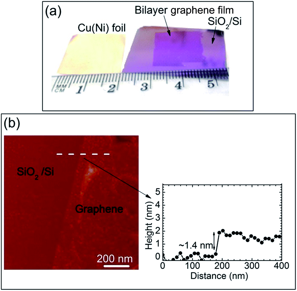 | ||
| Fig. 1 A continuous wafer-scale bilayer graphene film obtained using AP-CVD. (a) Photographs of the Cu (0.61 at% Ni) foil (∼20 × 20 mm2) with an as-grown bilayer graphene film and transferred bilayer graphene film on a 300 nm SiO2/Si substrate. (b) AFM image (showing the edge) of bilayer graphene transferred onto a SiO2/Si substrate and height profile measured along the dotted line. | ||
The SEM micrographs in Fig. 2(a) and (b) show uniform and continuous bilayer graphene film (at low and high magnifications respectively) obtained on a dilute Cu (0.61 at% Ni) foil and transferred onto a 300 nm SiO2/Si substrate. The area of the graphene film shown in the SEM micrographs in Fig. 2 is the same as those of other parts of the film (see Fig. S5 in the ESI†), suggesting a uniform and continuous graphene film over entire graphene film. In contrast, SEM micrographs of the bilayer graphene film obtained on pure Cu foil (Fig. S3 in the ESI†) shows non-uniform layers of graphene (lighter areas corresponding to monolayer and darker areas to multilayer (bilayer) graphene). Nonetheless, CVD synthesis of graphene on Cu favours monolayer graphene, hence its bilayer graphene shows bilayer domains on a monolayer graphene background.19 In the high magnification image (Fig. 2(b)), it can be seen that wrinkles due to graphene transfer are fewer in the bilayer graphene compared to monolayer graphene film transferred under identical conditions onto a 300 nm SiO2/Si substrate (see Fig. S1(a) in the ESI†).
 | ||
| Fig. 2 (a and b) SEM micrographs of a bilayer graphene film (at low and high magnifications respectively) obtained on a dilute Cu (0.61 at% Ni) foil and transferred onto a 300 nm SiO2/Si substrate. | ||
In the Raman spectrum of high-quality graphene, the main features that are observable are the G-band mode (∼1590 cm−1) and the 2D-band mode (∼2690 cm−1). The low intensity disorder-induced D-band (∼1350 cm−1) confirms the high-quality of graphene films.30–32 Fig. 3 shows the Raman data of a bilayer graphene film obtained on a dilute Cu (0.61 at% Ni) foil and transferred onto a 300 nm SiO2/Si substrate. In Fig. 3(a) and (b), the Raman optical microscope images (at low and higher magnifications respectively) also show a uniform and continuous graphene film over a large-area (analysed area) of graphene film obtained on a dilute Cu (0.61 at% Ni) foil in agreement with the photographic image (Fig. 1(a) for the sample transferred onto SiO2) and SEM images (Fig. 2). Fig. 3(b) shows a slightly higher contrast than that of a monolayer graphene (Fig. S1(b) in the ESI†) since the optical microscope images of graphene films display a colour contrast between monolayer and bi or multilayer graphene films. Fig. 3(c) shows the average Raman spectrum of spectra acquired from a 30 μm2 area (indicated with a square box in Fig. 3(b)) of a bilayer graphene film. In Fig. 3(c), the 2D peak full width at half maximum (FWHM) of 55.5 cm−1 compares well with the average values (53 cm−1,20 60.1 cm−1 (ref. 33) and 51 cm−1 (ref. 34)) obtained by others for AB-stacked bilayer graphene films.
 | ||
| Fig. 3 (a and b) Raman optical microscope images of a bilayer graphene film (at low and higher magnifications respectively) obtained on a dilute Cu (0.61 at% Ni) foil and transferred onto a 300 nm SiO2/Si substrate. (c) Average Raman spectrum of spectra acquired from a 30 μm2 area (indicated with a square box in (b)) of a bilayer graphene film. | ||
In the Raman spectrum of graphene, the 2D-band mode is adopted to distinguish between the numbers of layers contained in graphene sample and is also sensitive to the stacking order in few layers graphene samples.31–33 Fig. 4(a) and (b) show the mapping of the 2D peaks FWHMs and of the corresponding 2D to G peaks intensities ratio (I2D/IG) respectively of Raman spectra acquired from 30 μm2 areas of a bilayer graphene film obtained on a dilute Cu (0.61 at% Ni) foil. The 2D peaks FWHMs are in the range of 38–70 cm−1 (Fig. 4(a)), I2D/IG in the range of 0.8–2.5 (Fig. 4(b)) and the 2D peaks positions are in the range of 2685–2703 cm−1 (Fig. S6(c)†). Distinct from monolayer graphene features (Fig. S2 and Table S1 in the ESI†), these features demonstrate the characteristics of bilayer graphene. Similar results are obtained from other parts of the graphene film which suggest a continuous bilayer graphene film (Fig. S6 in the ESI†). Fang et al.33 have identified the AB-stacked bilayer graphene with 2D peaks FWHMs in the range of ∼40–70 cm−1 (with a cut-off FWHM of 70 cm−1) using a CVD graphene prepared on Cu foil.
 | ||
| Fig. 4 (a) The mapping of 2D peaks FWHMs and (b) of the corresponding 2D to G peaks intensities ratio (I2D/IG) for bilayer graphene film obtained on a dilute Cu (0.61 at% Ni) foil and transferred onto 300 nm SiO2/Si substrate. (c) Raman spectra from data mapped in (a) and the 2D peaks solid-lines are Lorentzians fits. | ||
The 2D peak in the Raman spectrum of graphene is a double-phonon resonant Raman process involving two in-plane transverse optical (iTO) mode phonons around the K-point.30–32 In monolayer graphene, the 2D peak has a single Lorentzian feature.30 In AB-stacked bilayer graphene the electronic band splits into two conduction and two valence bands and the split causes splitting of the phonon bands into two components which give rise to four peaks in the Raman 2D peak with peak frequencies at approximately 2655, 2680, 2700, and 2725 cm−1 and FWHMs equal to that of monolayer graphene.30 In AB-stacked bilayer graphene, these four peaks are fitted as four Lorentzians to the 2D peak in the Raman spectrum.30–32 The amplitudes of these four Lorentzians are relative, meaning, two Lorentzians at ∼2680 and ∼2700 cm−1 (inner peaks in 2D peak) have almost the same intensity and are higher than the other two at ∼2655 and ∼2725 cm−1 (outer peaks in 2D peak).32 For non-AB stacked bilayer graphene, the 2D peak is a single Lorentzian as in monolayer graphene, but with a larger FWHM and upshifted frequency from that of monolayer graphene.31 Fig. 4(c) shows the Raman spectra from data mapped in Fig. 4(a) and the 2D peaks were fitted with four Lorentzians which demonstrate features of AB-stacked bilayer graphene.
Table 1 shows a summary of the analysis results of the Raman spectra of monolayer and bilayer graphene films obtained on Cu (shown in the ESI†) and dilute Cu (0.61 at% Ni) foils. In this table, it can be seen that graphene features of bilayer graphene obtained on Cu foil overlap with those of monolayer graphene, suggesting the presence of a significant fraction of monolayer graphene in the prepared bilayer graphene film. In contrast to the bilayer graphene film obtained on Cu foil, the bilayer graphene film obtained on Cu (0.61 at% Ni) foil shows different features compared to monolayer graphene features as would be expected in Raman analysis of monolayer and multilayer (bilayer) graphene. The Raman spectral analysis showed that the bilayer graphene film obtained on the dilute Cu (0.61 at% Ni) foil is predominantly AB-stacked bilayer graphene and that was further supported by electron diffraction analysis.
| Graphene layers | CVD substrate | 2D peaks positions (cm−1) | 2D peaks FWHMs (cm−1) | 2D/G peaks |
|---|---|---|---|---|
| Monolayer | Cu foil | 2670–2682 | 28–36 | 2.5–4 |
| Bilayer | Cu foil | 2675–2703 | 28–53 | 0.8–4 |
| Bilayer | Cu (0.61 at% Ni) foil | 2685–2703 | 38–70 | 0.8–2.5 |
Fig. 5(a) shows a typical TEM image of the bilayer graphene film obtained on Cu (0.61 at% Ni) foil and transferred on a lacey carbon TEM grid (see Fig. S7(a) in the ESI† for the low magnification TEM image). In Fig. 5(a), regions A and B shown in a hole of a lacey carbon TEM grid show an area without graphene and with graphene respectively. Fig. 5(b) shows a typical high magnification TEM image of graphene in region B of Fig. 5(a), and (c) shows a SAED pattern from the corresponding area which shows two sets of hexagonal diffraction spots. TEM diffraction patterns were analysed using a diffraction ring profiler, which was developed for phase identification in complex microstructures.35 Fig. 5(d) shows the diffraction rings intensity profile which was indexed using the Miller–Bravais indices (hkil) for graphite where peaks at d = 1.23 Å and peak d = 2.13 Å in Fig. 5(d) correspond to indices (1−210) for outer hexagon and (1−110) for inner hexagon respectively.36 The electron diffraction patterns obtained at different positions of the graphene film show similar results (see Fig. S7 in the ESI†). It is known that the relative intensities of the spots in the outer hexagon are twice the intensities of the spots in the inner hexagon for AB-stacked bilayer graphene (shown with a schematic view in the figure inset).32,33,36 Therefore, the diffraction data (similar to that obtained from other spots of the same film) show that the graphene film obtained on dilute Cu (0.61 at% Ni) foil is predominantly AB-stacked bilayer graphene as evidenced by relative intensities shown in Fig. 5(d) in agreement with the Raman data above.
 | ||
| Fig. 5 (a) TEM image of bilayer graphene film obtained on Cu (0.61 at% Ni) foil and transferred onto a lacey carbon TEM grid (regions A and B shown in a hole of a lacey carbon TEM grid show an area without graphene and with graphene respectively). (b) A high magnification TEM image of graphene in region B of (a). (c) A selected area electron diffraction (SAED) pattern from an area shown in (b) and showing two sets of hexagonal diffraction spots. (d) The diffraction rings intensity profile of two sets of hexagonal diffraction spots in (c) and the inset to the figure shows a schematic view of the AB-stacked bilayer graphene and diffraction rings. | ||
A four-point probe/sheet resistance measuring system for thin films was used to measure the sheet resistance of the bilayer graphene film transferred onto the 300 nm SiO2/Si substrate and was obtained as 284 Ω sq−1 (see Fig. S8 in the ESI†). A sheet resistance of 284 Ω sq−1 measured for the bilayer graphene obtained on Cu (0.61 at% Ni) foil in this study is in the same order of magnitude with that measured from AB-stacked bilayer (287 Ω sq−1) graphene film in ref. 20.
Fig. 6(a) and (b) show the map images of TOF-SIMS secondary ion intensities measured from a dilute Cu (0.61 at% Ni) foil surface of the as-received sample (i.e. without surface sputtering with an ion gun) and after surface cleaning for 3 min with ion sputtering respectively. The foil was annealed under graphene growth conditions without methane source. Alfa Aesar Cu foil doped with Ni to obtain a dilute Cu (0.61 at% Ni) foil for graphene growth has a purity of 99.8% and about 0.2% unknown-impurities. The TOF-SIMS data (Fig. 6) shows the presence of Na, Al, Si, C2H5, K, Fe and Ni impurities in the Cu (0.61 at% Ni) surface and subsurface layers (bulk layers). These impurities have a potential to influence the CVD graphene growth and the effect of each impurity will be determined by its metal–carbon interaction energy, metal–methane decomposition rate and metal–carbon solubility. During CVD graphene growth at high temperatures (∼1000 °C), Na and K alkali-metals (and C2H5) will not dominate the surface due to their very low melting points (<100 °C). On the other hand, Al, Si and Fe impurities have bulk concentrations on the order of a few parts per million (<10 ppm) and Ni has 6100 ppm (0.61 at%) and hence Ni has a higher surface concentration than all other impurities detected with TOF-SIMS. In addition, Ni has strong metal–carbon atomic interaction, high metal–methane decomposition rate, high carbon solubility and as a result, Ni in the surface of a dilute Cu (0.61 at% Ni) foil will contribute significantly during the CVD graphene growth on Cu (0.61 at% Ni) foil. In brief, except for Ni which has very high bulk concentration of 6100 ppm, high relative intensities of Na, Al, Si, C2H5, K and Fe in Fig. 6 do not necessarily show high surface concentrations of these elements in Cu (0.61 at% Ni) foil since they have strong signals in TOF-SIMS.
 | ||
| Fig. 6 (a) The map images of TOF-SIMS secondary ion intensities measured from a dilute Cu (0.61 at% Ni) foil surface of the as-received sample (i.e. without surface sputtering with ion gun) and (b) after surface cleaning for 3 min with ion sputtering. The foil was annealed under graphene growth conditions without methane source. | ||
It is desirable to quantify the TOF-SIMS secondary-ion intensities measured; however, the quantification in TOF-SIMS is complicated because of the strong dependence of the secondary-ion yield on the matrix effects (target chemical and electronic character).37,38
Furthermore, the surface fractional concentration of Ni in the dilute Cu (0.61 at% Ni) foil with an as-grown bilayer graphene film was quantified with X-ray photoelectron spectroscopy. In the analysis, a resolved angle between the foil surface and the path to the analyzer focuses analysis within the topmost (∼5) atomic layers. In this instance, the topmost (∼5) atomic layers consist of two atomic layers of bilayer graphene and 2 atomic layers of Cu foil. The foil surface was sputter cleaned with ions for several cycles while measuring the spectra of elements, C 1s, Cu 2p, Ni 2p (shown in Fig. 7(a)–(c)) and O 1s after each sputter cycle, to obtain the chemical composition of the foil surface (Table 2). In Fig. 7 and Table 2, it can be seen that before surface sputter cleaning, C 1s have high concentrations compared to Cu 2p substrate, O 1s (adsorbed from air) and Ni 2p and that confirms a film of graphene on the foil surface. After a 2 min sputter cycle, Ni 2p shows a surface fractional concentration of 1.2 at% and the presence of C 1s and O 1s (restricted to the surface) suggest that the analysis is within the first atomic layer of a Cu foil (see Fig. 7 and Table 2).
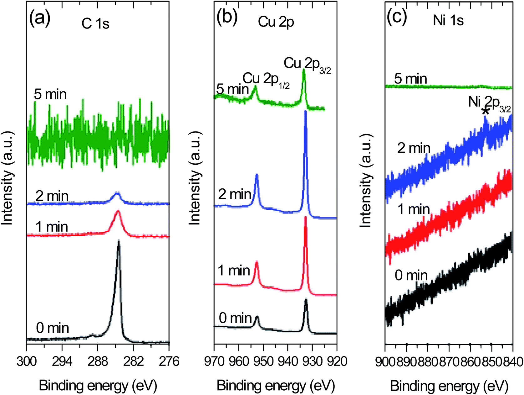 | ||
| Fig. 7 The XPS spectra of (a) C 1s, (b) Cu 2p and (c) Ni 2p after different sputter cycles of a dilute Cu (0.61 at% Ni) foil with as-grown bilayer graphene film. | ||
| Sputter cycles | C 1s (at%) | Cu 2p (at%) | O 1s (at%) | Ni 2p (at%) |
|---|---|---|---|---|
| 0 min | 54.9 | 28.0 | 17.1 | — |
| 1 min | 14.1 | 72.7 | 13.2 | — |
| 2 min | 6.5 | 83.0 | 9.3 | 1.2 |
| 5 min | — | 99.9 | — | — |
Interestingly, after a 5 min sputter cycle, Ni 2p, C 1s and O 1s are not detected and Cu shows a fractional concentration of 99.9 at% which correspond to a relatively pure Cu. In this instance, a 5 min sputter cleaning at a rate of 0.3 nm min−1 is equivalent to a removal of 1.5 nm thick material which in this instance consist of a bilayer graphene (∼1 nm thick including surface adsorbed carbon and oxygen from air) and approximately the first two atomic layers of Cu (∼0.5 nm). Accordingly, the analysis shown here after 5 min sputter cleaning are from the topmost subsurface atomic layers of Cu as confirmed by the absence (zero concentrations) of C 1s and O 1s which are restricted to the surface of Cu. In brief, this analysis confirms a surface alloying of Cu with Ni (similar to the TOF-SIMS data above) while maintaining relatively pure Cu in the topmost subsurface atomic layers of the Cu. However, a Ni surface fractional concentration of 1.2 at% should be larger than 1.2 at%, at least 2.1 at% as calculated in Fig. S9 in the ESI,† because 1.2 at% is the fractional/average value of Ni concentration measured in the presence of other species rather than Cu alone by XPS.
Fig. 8 shows the C 1s core level spectra of the as-grown bilayer graphene film on dilute Cu (0.61 at% Ni) foil. The fitted peaks, namely, sp2 C![[double bond, length as m-dash]](https://www.rsc.org/images/entities/char_e001.gif) C peak at 284.5 eV (graphene component), C–O–C peak at 286.2 eV, CO peak at 287.4 eV, O–CO peak at 289.4 eV (oxide components) and π–π* peak at 291.5 eV (satellite peak/electrons transition) were determined by reference to other studies.39–41 The fitted sp2 CC peak has a dominating intensity which confirms the sp2 hybridization property of graphene in the as-grown bilayer graphene film,30,41 the low-intensity oxide peaks could be due to adsorbed oxygen or carbon bonded oxygen during synthesis of the graphene film. The π–π* electrons transition enhances the carbon to carbon bonds in graphene and confirms the high quality of the graphene (suggested by the Raman data) since the π–π* bonds determine the fundamental electronic properties of graphene.30,40
C peak at 284.5 eV (graphene component), C–O–C peak at 286.2 eV, CO peak at 287.4 eV, O–CO peak at 289.4 eV (oxide components) and π–π* peak at 291.5 eV (satellite peak/electrons transition) were determined by reference to other studies.39–41 The fitted sp2 CC peak has a dominating intensity which confirms the sp2 hybridization property of graphene in the as-grown bilayer graphene film,30,41 the low-intensity oxide peaks could be due to adsorbed oxygen or carbon bonded oxygen during synthesis of the graphene film. The π–π* electrons transition enhances the carbon to carbon bonds in graphene and confirms the high quality of the graphene (suggested by the Raman data) since the π–π* bonds determine the fundamental electronic properties of graphene.30,40
 | ||
| Fig. 8 The high-resolution C 1s core level XPS spectra of as-grown bilayer graphene film on dilute Cu (0.61 at% Ni) foil. | ||
Conclusions
This study demonstrated the synthesis of a wafer-scale (on the scale of an entire foil) and high-quality AB-stacked bilayer graphene film on a dilute Cu (0.61 at% Ni) foil using AP-CVD. AFM, SEM, Raman, TEM/SAED and four-point probe/sheet resistance analysis showed that a bilayer graphene film obtained on a dilute Cu (0.61 at% Ni) foil is of high-quality, continuous (wafer-scale) and mainly Bernal stacked. This study clearly showed the capability of a dilute Cu (0.61 at% Ni) foil for growing a wafer-scale bilayer graphene film compared to a pure Cu foil which is known to grow bilayer domains on a monolayer graphene background in AP-CVD (see Fig. S3 and S4 in the ESI†). The capability of a dilute Cu (0.61 at% Ni) foil for growing a wafer-scale bilayer graphene film was ascribed to the carbon solubility and the metal surface catalytic activity of Cu and Ni in a dilute Cu (0.61 at% Ni) foil. In a dilute Cu (0.61 at% Ni) foil, a high surface concentration of Ni compared to a low bulk concentration of Ni was confirmed with TOF-SIMS and XPS.Acknowledgements
This work is based on research supported by the South African Research Chairs Initiative of the Department of Science and Technology and National Research Foundation (NRF) of South Africa (Grant No. 97994). M. J. Madito acknowledges the financial support from the university of Pretoria and NRF for his PhD studies. Mr W. A. Jordaan at NMISA is acknowledged for his assistance on the TOF-SIMS measurements. Dr N. Mathe and Ms R. Rikhotso at CSIR national centre for nano-structured materials are acknowledged for their assistance with the TEM/SAED measurements. Prof. Yury Gogotsi’s group at Drexel University is acknowledged for its assistance on the XPS measurements.References
- A. K. Geim and K. S. Novoselov, Nat. Mater., 2007, 6, 183–191 CrossRef CAS PubMed.
- M. Freitag, H. Chiu, M. Steiner, V. Perebeinos and P. Avouris, Nat. Nanotechnol., 2010, 5, 497–501 CrossRef CAS PubMed.
- F. Bonaccorso, Z. Sun, T. Hasan and A. C. Ferrari, Nat. Photonics, 2010, 4, 611–622 CrossRef CAS.
- F. Schwierz, Nat. Nanotechnol., 2010, 5, 487–496 CrossRef CAS PubMed.
- Y. Xue, B. Wu, Y. Guo, L. Huang, L. Jiang, J. Chen, D. Geng, Y. Liu, W. Hu and G. Yu, Nano Res., 2011, 4, 1208–1214 CrossRef CAS.
- W. J. Yu, L. Liao, S. H. Chae, Y. H. Lee and X. Duan, Nano Lett., 2011, 11, 4759–4763 CrossRef CAS PubMed.
- Y. Zhang, T. Tang, C. Girit, Z. Hao, M. C. Martin, A. Zettl, M. F. Crommie, Y. R. Shen and F. Wang, Nature, 2009, 459, 820–823 CrossRef CAS PubMed.
- C. Mattevi, H. Kim and M. Chhowalla, J. Mater. Chem., 2011, 21, 3324 RSC.
- L. Ma, W. Ren, Z. Dong, L. Liu and H. Cheng, Chin. Sci. Bull., 2012, 57, 2995–2999 CrossRef CAS.
- X. Li, W. Cai, J. An, S. Kim, J. Nah, D. Yang, R. Piner, A. Velamakanni, I. Jung, E. Tutuc, S. K. Banerjee, L. Colombo and R. S. Ruoff, Science, 2009, 324, 1312–1314 CrossRef CAS PubMed.
- A. Guermoune, T. Chari, F. Popescu, S. S. Sabri, J. Guillemette, H. S. Skulason, T. Szkopek and M. Siaj, Carbon, 2011, 49, 4204–4210 CrossRef CAS.
- A. Reina, S. Thiele, X. Jia, S. Bhaviripudi, M. S. Dresselhaus, J. A. Schaefer and J. Kong, Nano Res., 2009, 2, 509–516 CrossRef CAS.
- S. Y. Kwon, C. V. Ciobanu, V. Petrova, V. B. Shenoy, J. Bareño, V. Gambin, I. Petrov and S. Kodambaka, Nano Lett., 2009, 9, 3985–3990 CrossRef CAS PubMed.
- G. Imamura and K. Saiki, J. Phys. Chem. C, 2011, 115, 10000–10005 CAS.
- G. A. López and E. J. Mittemeijer, Scr. Mater., 2004, 51, 1–5 CrossRef.
- W. Liu, H. Li, C. Xu, Y. Khatami and K. Banerjee, Carbon, 2011, 49, 4122–4130 CrossRef CAS.
- W. Liu, S. Kraemer, D. Sarkar, H. Li, P. M. Ajayan and K. Banerjee, Chem. Mater., 2014, 26, 907–915 CrossRef.
- A. Mohsin, L. Liu, P. Liu, W. Deng, I. N. Ivanov, G. Li, O. E. Dyck, G. Duscher, J. R. Dunlap, K. Xiao and G. Gu, ACS Nano, 2013, 7, 8924–8931 CrossRef CAS PubMed.
- S. Bhaviripudi, X. Jia, M. S. Dresselhaus and J. Kong, Nano Lett., 2010, 10, 4128–4133 CrossRef CAS PubMed.
- S. Chen, W. Cai, R. D. Piner, J. W. Suk, Y. Wu, Y. Ren, J. Kang and R. S. Ruoff, Nano Lett., 2011, 11, 3519–3525 CrossRef CAS PubMed.
- A. Harpale, M. Panesi and H. B. Chew, J. Chem. Phys., 2015, 142, 061101 CrossRef PubMed.
- W. Cai, R. D. Piner, Y. Zhu, X. Li, Z. Tan, H. C. Floresca, C. Yang, L. Lu, M. J. Kim and R. S. Ruoff, Nano Res., 2009, 2, 851–856 CrossRef CAS.
- A. Reina, X. Jia, J. Ho, D. Nezich, H. Son, V. Bulovic, M. S. Dresselhaus and J. Kong, Nano Lett., 2009, 9, 30–35 CrossRef CAS PubMed.
- H. Choi, Y. Lim, M. Park, S. Lee, Y. Kang, M. S. Kim, J. Kim and M. Jeon, J. Mater. Chem. C, 2015, 3, 1463–1467 RSC.
- Y. Wu, H. Chou, H. Ji, Q. Wu, S. Chen, W. Jiang and Y. Hao, ACS Nano, 2012, 7731–7738 CrossRef CAS PubMed.
- N. Liu, L. Fu, B. Dai, K. Yan, X. Liu, R. Zhao, Y. Zhang and Z. Liu, Nano Lett., 2011, 11, 297–303 CrossRef CAS PubMed.
- Y. Wu, H. Chou, H. Ji, Q. Wu, S. Chen, W. Jiang, Y. Hao, J. Kang, Y. Ren, R. D. Piner and R. S. Ruoff, ACS Nano, 2012, 6, 7731–7738 CrossRef CAS PubMed.
- S. M. Kim, A. Hsu, Y.-H. Lee, M. Dresselhaus, T. Palacios, K. K. Kim and J. Kong, Nanotechnology, 2013, 24, 365602 CrossRef PubMed.
- M. Her, R. Beams and L. Novotny, Phys. Lett. A, 2013, 377, 1–3 CrossRef.
- Physics of Graphene, ed. H. Aoki and M. S. Dresselhaus, Springer, New York, 2014 Search PubMed.
- L. M. Malard, M. A. Pimenta, G. Dresselhaus and M. S. Dresselhaus, Phys. Rep., 2009, 473, 51–87 CrossRef CAS.
- A. C. Ferrari, J. C. Meyer, V. Scardaci, C. Casiraghi, M. Lazzeri, F. Mauri, S. Piscanec, D. Jiang, K. S. Novoselov, S. Roth and A. K. Geim, Phys. Rev. Lett., 2006, 97, 187401 CrossRef CAS PubMed.
- W. Fang, A. L. Hsu, R. Caudillo, Y. Song, A. G. Birdwell, E. Zakar, M. Kalbac, M. Dubey, T. Palacios, M. S. Dresselhaus, P. T. Araujo and J. Kong, Nano Lett., 2013, 13, 1541–1548 CAS.
- S. Lee, K. Lee and Z. Zhong, Nano Lett., 2010, 10, 4702–4707 CrossRef CAS PubMed.
- L. Zhang, C. M. B. Holt, E. J. Luber, B. C. Olsen, H. Wang, M. Danaie, X. Cui, X. Tan, V. W. Lui, W. P. Kalisvaart and D. Mitlin, J. Phys. Chem. C, 2011, 115, 24381–24393 CAS.
- A. Dato, V. Radmilovic, Z. Lee, J. Phillips and M. Frenklach, Nano Lett., 2008, 8, 2012–2016 CrossRef CAS PubMed.
- A. M. Belu, D. J. Graham and D. G. Castner, Biomaterials, 2003, 24, 3635–3653 CrossRef CAS PubMed.
- R. G. Wilson, J. Appl. Phys., 1988, 63, 5121 CrossRef CAS.
- Y. V. Butenko, S. Krishnamurthy, A. K. Chakraborty, V. L. Kuznetsov, V. R. Dhanak, M. R. C. Hunt and L. Šiller, Phys. Rev. B: Condens. Matter Mater. Phys., 2005, 71, 075420 CrossRef.
- M. Hsiao, S. Liao, M. Yen, C. Teng, S. Lee, N. Pu, C. Wang, Y. Sung, M. Ger, C. Ma and M. Hsiao, J. Mater. Chem., 2010, 20, 8496 RSC.
- S. Ogawa, T. Yamada, S. Ishidzuka, A. Yoshigoe, M. Hasegawa, Y. Teraoka and Y. Takakuwa, Jpn. J. Appl. Phys., 2013, 52, 110122 CrossRef.
Footnote |
| † Electronic supplementary information (ESI) available: Characterisation or results of monolayer and bilayer graphene films obtained on pure Cu foils. See DOI: 10.1039/c5ra27159b |
| This journal is © The Royal Society of Chemistry 2016 |