Fabrication and surface stochastic analysis of enhanced photoelectrochemical activity of a tuneable MoS2–CdS thin film heterojunction

M. Ziraka, M. Ebrahimia, M. Zhaob, O. Moradlouc, M. Samadia, A. Bayata, H.-L. Zhang*b and A. Z. Moshfegh*ad
aDepartment of Physics, Sharif University of Technology, P.O. Box 11555-9161, Tehran, Iran. E-mail: moshfegh@sharif.edu
bState Key Laboratory of Applied Organic Chemistry, College of Chemistry and Chemical Engineering, Lanzhou University, Lanzhou 730000, P. R. China. E-mail: Haoli.zhang@lzu.edu.cn
cDepartment of Chemistry, Alzahra University, P.O. Box: 1993893973, Tehran, Iran
dInstitute of Nanoscience and Nanotechnology, Sharif University of Technology, P.O. Box 14588-8969, Tehran, Iran

Received 11th December 2015 , Accepted 2nd February 2016

First published on 3rd February 2016


Abstract

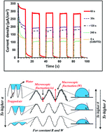
A very simple and well-controlled procedure was employed to prepare CdS nanoparticle/few-layer MoS2 nanosheet/Indium tin oxide (ITO) thin film heterostructures. To tune and fabricate the CdS/MoS2(t)/ITO thin films with various surface topographies, first electrophoretic deposition (EPD) was used to deposit MoS2 nanosheets on the ITO substrate under an optimized applied potential difference (8 V) for different deposition times (t) of 30, 60, 120 and 240 s. Then, CdS nanoparticles were deposited via a successive ion layer adsorption and reaction (SILAR) technique. The highest photo-current density of 285 μA cm−2 was measured for the CdS/MoS2(60 s)/ITO sample, which was about 2.3 times higher than the value obtained for bare CdS/ITO. The photo-enhancement mechanism of the CdS/MoS2(t)/ITO heterostructures was described using a stochastic model. The results show that the CdS/MoS2(60 s)/ITO electrode exhibits the highest roughness exponent (2α = 0.67) with the smoothest nanometric fluctuations, resulting in the best wetting properties, and thus, the highest interaction between the electrolyte and the sample surface, leading to the highest PEC activity. On the other hand, the samples with small α possess rough and nanometric-jagged fluctuations. The air trapping inside these microscopic surface fluctuations reduces the wettability as well as surface interaction between the sample and the electrolyte, resulting in low photo-current density.


1. Introduction

In recent years, accompanying the fascinating properties of graphene and its booming development, rapidly growing research interest and scientific attention has been focused on the other ultrathin 2D crystals. In particular, there is at present an increasing interest in transition metal dichalcogenides (TMDs) due to their potential for a wide range of applications.1–3 TMDs have the general formula of X–M–X (M is a transition metal such as Mo, W, Ti, V, and X is a chalcogen such as S and Se), in which two hexagonally-arranged X planes are separated by the same hexagonal metal plane. Inside each X–M–X layer, the atoms are bonded together covalently and adjacent layers stack over each other via weak van der Waals force.4 This weak interlayer force allows to easily exfoliating the bulk TMDs into atomically thick 2D nanosheets. These 2D crystals can improve the intrinsic properties of their bulk form and introduce a completely new and fascinating range of properties.

Of particular interest, 2D-MoS2 (the most famous and abundant member of TMDs) nanosheets have exhibited unique properties and applications such as hydrogen evolution reaction,5–7 nonlinear optical applications,2,8 field effect transistor,9,10 high performance lithium and sodium ion batteries,11–13 photoluminescence and bioimaging14 and so on.

It has been reported that MoS2 low dimensional nanostructures exhibit photo-responsivity due to their suitable band gap for solar spectrum absorption (MoS2 mono-layer is a direct band gap semiconductor with energy band gap of Eg ∼1.9 eV (ref. 15)) and photocatalytic stability against photocorrosion.16,17 many studies have reported the photocatalytic activity of MoS2 nanostructures toward water pollutant degradation,18,19 photocatalytic hydrogen production20,21 and photoelectrochemical activity,17 indicating promising potentials of MoS2 2D-nanosheets for solar energy harvesting and conversion.

Among various photo-active materials, CdS has been the subject of many interests because of its low cost and simple preparation methods for various applications.19,22 More importantly, CdS has a narrow direct band gap with Eg = 2.4 eV,23 making it a well-known photo-active material under visible light. However, bare CdS suffers from low photocatalytic activity and low stability under sunlight irradiation. To overcome these drawbacks, noble metal co-catalysts such as Pt, Pd, and Au are often used to improve its catalytic activity and stability.24,25 But, using noble metal co-catalyst is limited due to their high cost and scarcity. So, it is very interesting to find a low cost but effective alternative co-catalyst to improve CdS visible photo-activity and its stability against photocorrosion.

Recently, MoS2 nanostructures have been shown as a promising low cost co-catalyst to enhance CdS photocatalytic activity toward hydrogen production.25–28 Zong et al. have experimentally confirmed that photocatalytic activity of MoS2-loaded CdS is even higher than that of Pt/CdS under the same reaction conditions.25,29 Chen et al. have also obtained H2 evolution rate up to 1315 μmol h−1 using the MoS2/CdS photocatalyst which was much higher than 488 μmol h−1 reported for Pt/CdS photocatalyst.26

Although many fascinating photocatalytic results have been reported for MoS2–CdS hetero-structure, but, low-cost, easy and safe preparation method to obtain MoS2–CdS thin films and their photoelectrochemical (PEC) performance has been rarely investigated, and the PEC property of the MoS2–CdS thin film is still in its infancy. Specially, to the best of our knowledge, the effect of MoS2–CdS thin film topography on its PEC performance has not been reported, yet.

We have demonstrated in our recent reports that investigation of surface topography from a stochastic point of view, provides very useful information to understand various properties of prepared thin films such as field emission property30 and photoelectrochemical performance.31,32 Herein, for the first time, we have carefully explored the correlation between stochastic topographic properties and PEC performance of CdS/MoS2/ITO thin films. To do that, we have employed a facile, well-controlled, completely safe and straight forward procedure to prepare CdS/MoS2 thin films on indium tin oxide (ITO) substrate with tuneable surface topographies. At the end, a mechanism was suggested based on the surface stochastic analysis and the contact angle (CA) measurements. The proposed model can provide a guidance to prepare the CdS/MoS2/ITO thin film with specific surface topography and proper wettability leading to the highest PEC performance toward hydrogen production under sunlight irradiation.

2. Experimental and methods

2.1 Materials

Deionized water purified with Milli-Q System (Millipore, Billerica, MA, USA) was used during all preparation procedures. All other materials were commercially provided and used without any further purification. These are including: absolute ethanol (Rionlon Chemical Reagent Inc., China), indium tin oxide (ITO) sheets (30 Ω □−1), bulk MoS2 powder (1–6 μm diameter, Aladdin Reagent Inc., China), sodium sulphide (Na2S·9H2O, 98%, Tianjin Guangfu Fine Chemical Institute, China), cadmium nitrate (Cd(NO3)2·4H2O, 99%, Beijing Chemical Reagent Research Institute, China).

2.2 Few-layer MoS2 solution preparation

Based on our previous report,33 mixed-solvent strategy was used to prepare few-layer MoS2 solution. In brief, 250 mg of bulk MoS2 was dispersed into 50 mL mixed water[thin space (1/6-em)]:[thin space (1/6-em)]ethanol solution with the volume fraction of water/ethanol = 55/45. After 30 min stirring, the solution was sonicated for 15 h in a common bath sonicator. The sonicated solution was maintained in room condition for 48 h. Then the 2/3 of the supernatant of the solution was collected and centrifuged at 3800 rpm for 45 min.

2.3 Thin film preparation

Electrophoretic deposition method was employed to deposit MoS2 nanosheets. Two pre-cleaned ITO sheets were placed in parallel manner with distance of 15 mm inside the few-layer MoS2 solution. The optimized electrical potential of 8 V was applied between these two ITO electrodes for different deposition times (t) namely 30, 60, 120, and 240 s. After preparation of MoS2(t)/ITO thin films, the CdS nanoparticles were deposited on the layers via successive ion layer adsorption and reaction (SILAR) method. The layers were immersed into 50 mM Cd(NO3)2 and then in 50 mM Na2S aqueous solutions for 20 s. These two immersion steps were named as a SILAR cycle. The samples were rinsed with DI water between each immersion step. 20 SILAR cycles were repeated to obtain CdS/MoS2(t)/ITO thin films.

2.4 Photoelectrochemical measurements

The PEC results were obtained by using a three-electrode setup connected to a CHI 660D electrochemical workstation (Shanghai Chenhua Instrument Co., China). In this setup, the synthesized CdS/MoS2(t)/ITO thin films were used as working electrode, a saturated calomel electrode (SCE) as the reference electrode and a platinum wire as the counter electrode. All the electrodes were put into 50 mM Na2S aqueous solution as electrolyte and 0.1 V bias voltage was applied during all PEC tests. The same electrolyte was also used to carry out the electrochemical impedance spectroscopy (EIS) measurements with the AC voltage amplitude of 5 mV and the voltage frequency ranging from 100 kHz to 1 Hz. The EIS data were obtained under 3 W Xe lamp irradiation.

2.5 Material characterization

Atomic force microscopy AFM (Agilent SPM 5500, USA) in tapping-mode was used to identify the MoS2 nanosheets lateral size and thickness and the results were analysed by “WSxM 5.0 Develop 7.0” software.34 Surface topographies of the layers were investigated under the same conditions reported in our previous works.30,31,35 PGENERAL T6 spectrophotometer was utilized to obtain the UV-visible absorption spectra of the samples. To study nanostructure morphology and chemical composition of the prepared thin films, Tecnai-G2-F30 (USA) high resolution transmission electron microscope (HRTEM) was employed. Raman microscopy (Invia Renishaw, UK, exciting laser wavelength of 514.5 nm) was also used to identify the composition of the samples. Si Raman peak at 520 cm−1 was the reference for Raman spectra calibration.

2.6 Surface stochastic analysis

Surface stochastic analysis was used for better understanding of the surface topography effects on PEC activities of the samples. Most common concepts for stochastic study of a surface (two dimensional substrate of size L × L) are the mean height of growing film [h with combining macron], its surface roughness W and roughness exponent α defined by the following expressions:36
 
image file: c5ra26487a-t1.tif(1)
 
W(L, t) = (〈[h[h with combining macron]]2〉)1/2 (2)
where t and [x with combining right harpoon above (vector)] are the deposition time and lateral coordinate, respectively. The averaging over different realizations of the sample position is represented by notation of 〈…〉.

Surface structure function, S([r with combining right harpoon above (vector)]), is used to measure the roughness exponent of a surface. This function depends on the length scale of Δ[x with combining right harpoon above (vector)] = [r with combining right harpoon above (vector)] and is defined as:35

 
S([r with combining right harpoon above (vector)]) = 〈|h([x with combining right harpoon above (vector)] + [r with combining right harpoon above (vector)]) − h([x with combining right harpoon above (vector)])|2 (3)
Height–height correlation function for a stationary surface, C(r), is related to the surface structure function as follows:
 
S(r) = 2W2(1 − C(r)) (4)
C(r) is defined by the correlation length η and the roughness exponent α (Hurst exponent) as is shown below:35
 
image file: c5ra26487a-t2.tif(5)
Replacing eqn (5) into (4) and expand it for small r, the second order structure function S(r) scales with r as following:35
 
S(r) ∼ rα (6)

The roughness exponent α normally ranges between 0 and 1 (0 < α < 1), and it is defined within the context of a microscopic limit (L → 0). According to eqn (5), for times much larger than saturation time, smaller roughness exponent corresponds to a very rough and jagged surface (high microscopic fluctuation). On the other hand, a surface with the larger roughness exponent possesses a smoother texture.30,37 More information and detailed discussions about these parameters can be found elsewhere.36 These concepts will be used to correlate the variation of surface roughness and topography of the deposited thin films and generated photo-current densities from the CdS/MoS2(t)/ITO thin films during PEC process.

3. Results and discussion

3.1 Exfoliated MoS2 nanosheets

Fig. 1 shows the UV-visible absorption spectrum of the MoS2 few-layer solution. Obvious absorption peaks can be seen which are labelled as A, B, C and D peaks. A and B located at 676 and 619 nm, are excitonic transitions arising from spin–orbit splitting of K point of the Brillouin zone at the top of valence band (VB).15 C and D excitonic peaks located at 450 and 400 nm are related to interband transitions from the occupied dz2 orbital to unoccupied dxy, x2y2 and dxz, yz orbitals.17
image file: c5ra26487a-f1.tif
Fig. 1 UV-visible absorption spectrum of exfoliated MoS2 solution, the inset is the photograph of the corresponding MoS2 solution.

It is clear that absorption of MoS2 nanosheets increases from 800 to 400 nm (visible solar region) and decrease in UV region (400 to 200 nm), which indicates that MoS2 flakes are very good candidates for photovoltaic and photocatalytic application in visible region of solar spectrum. In the photovoltaic related studies, sun light transmission is also an important parameter which determines the output photocurrent density of the materials. Therefore the corresponding UV-visible transmittance of the obtained MoS2 solution has been depicted in Fig. S1 of ESI. The absorption spectrum and light-brownish colour of the exfoliated solution (Fig. 1 inset) are in good agreement with standard UV-visible absorption spectrum for 2H-MoS2 semiconducting phase,17,38 indicating that no crystal change occurred during our proposed preparation procedure.

AFM analysis was also employed to explore the dimensions of the final MoS2 flakes. A 2D-AFM image has been shown in Fig. 2a and height profiles of some selected flakes have been also plotted. As it can be seen, there is a distribution of flakes sizes between about 30 and 150 nm. The thicknesses of flakes have also a distribution between about 1 and 15 nm. It is well known that the flakes with the same size and thickness cannot be obtained by sonication–exfoliation methods and the final products have a distribution in thickness and size.39–41 Herein, the MoS2 nanosheets obtained via mixed-solvent strategy (a type of sonication–exfoliation methods) show the same behaviour too. The average thickness and lateral dimension of the flakes were measured to be ∼5 and ∼60 nm, respectively.


image file: c5ra26487a-f2.tif
Fig. 2 (a) 2D-AFM image and selected height profile of the MoS2 flakes on mica substrate. (b) TEM image of exfoliated MoS2 nanosheets.

It was reported that a monolayer MoS2 prepared via chemical exfoliation methods is about 0.8–1.2 nm thick.15,42 Based on these findings, it is estimated that the prepared MoS2 flakes contain 6 layers in average. It is worth to note that there are also many single-layer nanosheets in the final solution. The population of these single-layer flakes can be increased via higher speed centrifugation and appropriate filtrations.

The dimensions of the flakes were also investigated through direct observation via TEM analysis. The TEM image (Fig. 2b) clearly shows the MoS2 nanosheets with an average of 60 nm in lateral size, confirming our AFM results. These results indicate that our utilized method can be manipulated to obtain both few-layer and single-layer MoS2 nanosheets.

3.2 CdS/MoS2(t)/ITO thin films

After deposition of MoS2 flakes on the ITO substrate by EPD technique at various deposition times followed by CdS loading via SILAR method, the obtained CdS/MoS2(t)/ITO layers were analysed by UV-visible transmission spectroscopy. Fig. 3 shows the UV-visible transmittance spectra of the thin films. As it can be seen, all of the CdS/MoS2(t)/ITO thin films have lower transmittance than the bare CdS/ITO as it was expected. The CdS/ITO thin film has an absorption edge at ∼500 nm. The bulk CdS thin film exhibits an absorption edge at 520 nm.43 Thus, the observed blue-shift indicates that the obtained CdS/ITO thin film contains CdS nanostructures with the average dimension of ∼10 nm.43,44 A second absorption edge appears at ∼680 nm in the CdS/MoS2(t)/ITO thin film which it is absent in the bare CdS/ITO layer. This absorption edge is related to peak A as excitonic transition in 2H-MoS2 layer, as discussed before (see Section 3.1 and Fig. 1). Inspecting the Fig. 3 indicates that the addition of MoS2 few-layer nanosheets to the CdS/ITO thin film, increases the light intensity absorption and also extends the absorption edge from 500 nm to ∼700 nm, which are in favour of CdS thin film photo-activity enhancement under visible light. Similar observations have been also reported elsewhere for CdS–MoS2 (ref. 45) and CdS–WS2 heterostructures.46
image file: c5ra26487a-f3.tif
Fig. 3 UV-visible transmittance spectra of the bare CdS/ITO and the CdS/MoS2(t)/ITO thin films prepared at various EPD times (t).

Raman spectroscopy was employed to determine the crystal phase composition of the final obtained thin films. Fig. 4a shows the Raman spectrum of the CdS/MoS2(60 s)/ITO thin film. Two obvious Raman peaks at 300 and 600 cm−1 are related to two characteristic CdS longitudinal optical (LO) phonon modes named 1LO and 2LO, respectively.47,48 The 1LO phonon peak for a single crystal of bulk CdS has been reported at peak position of 305 cm−1, while it has been observed at ∼300 cm−1 for CdS nanostructures.49,50


image file: c5ra26487a-f4.tif
Fig. 4 (a) Raman spectrum of the CdS/MoS2(60 s)/ITO thin film (b) TEM image and (c) corresponding HRTEM image of the CdS–MoS2 heterojunction structure.

The observed red shift of the 1LO Raman peak in the CdS/MoS2(t)/ITO thin films compared with the bulk CdS is due to the phonon confinement effect49 and this observation is consistent with other reports for 1LO peak in CdS nanoparticles (d ∼ 4–10 nm).47,51

It is well known that there are four active first-order Raman modes observed in bulk 2H-MoS2 Raman spectra, namely, E1g (286 cm−1), E12g (383 cm−1), A1g (407.5 cm−1), and E12g (32 cm−1).52,53 The E1g mode is forbidden in the back scattering configuration. The E22g mode cannot be accessible for conventional Raman apparatuses due to the constraint of Rayleigh line rejection filter (>100 cm−1).54 Thus, the MoS2 Raman spectrum is dominated by E12g and A1g modes. These two peaks are clearly observable at 383.5 and 407.2 cm−1, indicating the presence of 2H-MoS2 few layers in the final thin films.

Li et al. have reported that Raman frequencies of E12g and A1g peaks vary monotonically with the layer number of ultrathin MoS2 flakes and can be used as reliable features to identify the MoS2 layer number.54 Using A1g peak position, the following exponential fitting model can be used to estimate the average number of layers:

 
ωA1g(N) = ωbulk + (ω1Lωbulk)exp[−χ(N − 1)] (7)
where N is the number of layers, χ the fitting parameter and ωbulk = 407.5 cm−1, ω1L = 403 cm−1 and ωA1g are bulk, mono-layer and measured A1g peak position of MoS2, respectively. After fitting the model to the data reported for various MoS2 thicknesses,53–55 χ = 0.508 was obtained. Inserting this parameter into the exponential fitting model, the average number of layers for ωA1g(N) = 407.2 cm−1 was estimated to be ∼6 layers. The obtained thickness of MoS2 nanosheets is in agreement with the AFM observations.

Raman mapping is a powerful technique to characterize the uniformity of the 2D materials and it helps to understand the large scale quality and uniformity of the final products surfaces. Fig. S2 shows the Raman mapping images, obtained for CdS(1LO) and MoS2(A1g) Raman signal of the CdS/MoS2(60 s)/ITO sample. It is clear from Fig. S2 that the ITO electrode surface has been completely covered with deposited materials (MoS2 and CdS) with nearly the same thickness in large scale. As it was mentioned before (Fig. 2a related discussions), the sonication–exfoliation methods cannot provide 2D materials with exactly the same thicknesses and sizes. 2D flakes obtained by these methods have a distribution in both thickness and lateral dimension.39,40,56 Thus, it was expectable that the obtained Raman mapping images for our synthesized samples do not have the same colour in different sample area. The AFM results also confirm that the flakes do not have the same size and thickness (Fig. 2a).

In addition of Raman mapping, SEM analysis was also used to monitor surface morphology changes and to confirm if the MoS2 and CdS can completely cover whole ITO surface with acceptable uniform deposition thickness. The obtained SEM images of bare ITO, MoS2/ITO, CdS/ITO and CdS/MoS2(60 s)/ITO electrodes have been shown as Fig. S3 (ESI). The obtained SEM images confirm that the materials have been deposited uniformly on ITO surface for all of the electrodes, which is in consistent with Raman mapping results.

TEM analysis was used to clearly verify the formation of atomic-heterojunction between the CdS nanoparticles and MoS2 nanosheets. The CdS/MoS2(60 s)/ITO electrode was razed carefully with a keen knife and sonicated in DI water for 30 min. The resulted suspension was dropped on carbon-coated Cu grid and subjected to TEM analysis. The results have been shown in Fig. 4b and c. Fig. 4b shows that the CdS nanoparticles with an average diameter of ∼10 nm have been deposited on the MoS2 sheets, confirming Raman and UV-visible absorption results.

The measured sizes of the deposited CdS nanoparticles are also in good agreement with our previous reports on CdS nanoparticles obtained via SILAR methods.43,44 The hexagonal arrangement of atoms in MoS2 nanosheets as well as the CdS (112) planes can be clearly observed in Fig. 4c. Therefore, Raman and TEM results strongly confirm that we have successfully fabricated CdS–MoS2 atomic hetero-junction, using our simple combined procedure without any crystal changes and any oxidation.

To evaluate and compare photoelectrochemical activity of the different CdS/MoS2(t)/ITO thin film heterostructures, the photo-current densities (J) generated by the samples under similar photo-irradiation condition (500 W Xe lamp light with intensity of 55 mW cm−2) were measured. The results have been presented in Fig. 5 and Table 1.


image file: c5ra26487a-f5.tif
Fig. 5 The measured photo-current density versus irradiation time of the various CdS/MoS2(t)/ITO thin films prepared with different EPD time.
Table 1 Photo-current density (J) and topographical properties of the CdS/MoS2(t)/ITO thin films with different deposition times (t)
Sample Surface ratio (Ar) Rct (Ω) J (μA cm−2) Hurst exponent (2α) Contact angle (°)
CdS/ITO 1.02 ± 0.02 2365 ± 70 125 ± 4 0.33 ± 0.03 91 ± 3
CdS/MoS2(30 s)/ITO 1.03 ± 0.01 1144 ± 35 197 ± 6 0.42 ± 0.02 83 ± 1
CdS/MoS2(60 s)/ITO 1.11 ± 0.01 1467 ± 50 285 ± 8 0.67 ± 0.04 68 ± 3
CdS/MoS2(120 s)/ITO 1.15 ± 0.03 2155 ± 70 177 ± 5 0.58 ± 0.03 83 ± 2
CdS/MoS2(240 s)/ITO 1.06 ± 0.02 3317 ± 110 105 ± 4 0.57 ± 0.02 85 ± 2


Fig. 5 shows the measured J as a function of irradiation time (Jt curve). It was found that all the CdS/MoS2(t)/ITO thin films except CdS/MoS2(240 s)/ITO have higher photo-current densities as compared with the bare CdS/ITO layer (125 μA cm−2). The sample prepared with 30 s of MoS2 deposition shows a higher J value (197 μA cm−2) as compared to the bare CdS/ITO. Further increasing MoS2 deposition time to 60 s, results in increase of J up to 285 μA cm−2. This is about 2.3 times greater than the value for the bare CdS/ITO thin film.

The results show that charge separation and transfer condition is improved when CdS makes an appropriate junction with MoS2 nanosheets. It can be understood more clearly by measuring and comparing the rise times and fall times of the as-prepared CdS/MoS2(60 s)/ITO structure and traditional CdS/ITO layers. The rise time is defined as the time that the photocurrent reaches to 90% of its stable value from dark current value upon light irradiation and the fall time is known as the time needed for the current value to drop to 10% after the light was turned off.57 Accordingly, the rise and fall times of the CdS/MoS2(60 s)/ITO and the CdS/ITO was measured and the results have been shown and compared in Fig. S4.

Rise times were determined to be 180 ± 10 and 210 ± 10 ms and the fall times were obtained to be 300 ± 10 and 380 ± 10 ms for the CdS/MoS2(60 s)/ITO and the CdS/ITO, respectively. The shorter rise and fall times for the CdS–MoS2 sample show that the photo-sensitivity of CdS layer has been improved when a junction is made with MoS2 nanosheets, which is very beneficial for many applications such as photo-detectors and sensors.58–60

3.3 Photo-enhancement mechanism

There are some reports discussing on the photo-activity of the CdS–MoS2 heterojunction, and some reasons have been explained for photo-activity enhancement of CdS after junction forming with MoS2.25,27,61 Herein, for the first time, we have investigated the PEC performance of the CdS/MoS2(t)/ITO thin films from surface stochastical and topographical point of view, accompanying with other important factors concerning. One of the most important factors influencing the photo-current density of a layer is its charge transfer resistance (Rct). This parameter was evaluated by using electrochemical impedance spectroscopy (EIS) measurements with amplitude of 5 mV and frequencies ranging from 100 kHz to 1 Hz.

The Nyquist plots for the synthesized samples were obtained under 3 W Xe lamp light photo-irradiation, and the results have been shown in Fig. 6 after compensation of the solution resistance. The Rct values are extracted by fitting the Nyquist plots data with equivalent Randles circuit via Z view software, and the obtained values have been listed in Table 1. As it can be seen, deposition of MoS2 nanosheets initially reduced the charge transfer resistance of the CdS/ITO thin films. But, increasing the EPD time resulted in increase in the MoS2 loading, and consequently, the Rct in the CdS/MoS2(t)/ITO thin films was increased as it was expected. Therefore, lower Rct in some CdS/MoS2(t)/ITO thin films (t = 30 and 60 s) as compared with CdS/ITO layer is a good reason for the obtained higher photo-current density. Concerning only Rct, the CdS/MoS2(60 s)/ITO (with higher Rct) should exhibit a lower photo-current density than the CdS/MoS2(30 s)/ITO sample. But we have observed an opposite situation. Therefore, charge transfer resistance is not the only decisive factor influencing the photo-activity of the CdS/MoS2(t)/ITO thin films.


image file: c5ra26487a-f6.tif
Fig. 6 Nyquist plots of the CdS/MoS2(t)/ITO thin films obtained for different MoS2 deposition times (t) under 3 W Xe lamp light.

Thin films with higher surface area are beneficial for higher photo-current generation as they have more active sites upon light harvesting and as a result, more reactions sites. The root mean square (rms) surface roughness (W) and surface area ratio (Ar) are useful parameters to compare the surface area of the layers. These two parameters have been evaluated and presented in Table 1 for the samples, based on our AFM data analysis.

2D-like structure of few-layer MoS2 has very high surface area. So, it is expected that MoS2 deposition increases the surface area of CdS layer and all the CdS/MoS2(t)/ITO thin films have more surface area as compared with the CdS/ITO sample. MoS2 deposition for 30 s resulted in slightly increase of rms surface roughness from 6.6 nm in the CdS/ITO to 7.1 nm for CdS/MoS2(30 s)/ITO. But the deposition of MoS2 for 60 s significantly increased the surface roughness to 20.1 nm which is about 3 times greater than the bare CdS/ITO thin film. Longer deposition of MoS2 for t > 60 s reduced the surface roughness from 20.1 nm for the CdS/MoS2(60 s)/ITO sample to 19.5 and 17 nm for the CdS/MoS2(120 s)/ITO and CdS/MoS2(240 s)/ITO thin films, respectively.

The obtained highest photo-current density (J) for the highest surface roughness (W) is logical and well accepted. The CdS/MoS2(60 s)/ITO and the CdS/MoS2(120 s)/ITO samples have nearly the same value of W in the range of our data error bar (±0.5 nm), but the former photo-current density is much higher that the latter one. The obtained higher Rct for the CdS/MoS2(120 s)/ITO is one of the reasons for its lower J. Concerning only Rct, when charge transfer resistance of the CdS/MoS2(60 s)/ITO increased from 1467 Ω to 2155 Ω in the CdS/MoS2(120 s)/ITO, the J should be decreased from 285 to 194 μA cm−2. But the obtained J for the CdS/MoS2(120 s)/ITO is 177 μA cm−2. This means that increasing Rct cannot be responsible for such significant photo-current reduction.

To understand the other reasons, a better criterion than W, namely the surface area ratio (Ar) of the samples should be compared. This parameter has been evaluated for the samples and reported in Table 1.

The Ar values show more unusual results. The CdS/MoS2(120 s)/ITO layer has higher Ar than the CdS/MoS2(60 s)/ITO but its photo-current density has a lower value. So, another scenario should be considered for the PEC performance of the synthesized samples.

The W and Ar are representations of macroscopic surface properties of the samples. To better understand the thin film properties, some microscopic surface parameters should be evaluated. Based on our previous studies,30,31 Hurst exponent (α) which is obtained based on stochastic analysis can provide very useful information to understand microscopic properties of a surfaces. Surface structure function, S(r), is calculated according to eqn (3) using raw AFM data. To do that, various places of the samples with area of 2 μm × 2 μm and resolution of 256 × 256 pixels were scanned by the AFM tip to obtain the h(x) for each pixel. The used AFM instruments and conditions were similar to our previous works.30,31,35

The obtained S(r) spectra have been plotted as a function of r in Fig. S5. The plots show that the structure functions of the samples become saturated in large r values (more than 100 nm). For small r, we can scale S(r) with r to calculate the corresponding Hurst exponent α (eqn (6)). The obtained α for various CdS/MoS2(t)/ITO thin films have been listed in Table 1. As it can be seen, MoS2 nanosheets deposition resulted in increasing α to reach its highest value (2α = 0.67) for the CdS/MoS2(60 s)/ITO. After that, the roughness exponent decreased and reached approximately to its saturated value for samples prepared with 120 and 240 s EPD. The stochastic analysis data show that the highest photo-current density is related to the samples with the greatest roughness exponent. As discussed before, two samples of the CdS/MoS2(60 s)/ITO and the CdS/MoS2(120 s)/ITO have almost the same W, and thus Rct cannot be responsible for this significant difference between the photo-current densities of these samples. Thus, it seems that the microscopic parameter of α, is playing an important role in the PEC performance of the layers.

Based on the above discussions, the mechanism of enhanced PEC activity of the samples can be proposed as following: (i) interface state effect plays an important role in the heterojunction properties, and makes a crucial effect on photovoltaic, photocatalytic and photoelectrochemical properties of CdS/MoS2(t)/ITO thin films. The nature and properties of the materials interface influence on charge separation and transport and consequently on photo-current density (J) of the photo-active materials. (ii) On the other hand, surface morphology and topography can also influence on the samples photo-activity. Therefore, J can be assumed as a function of interface states and morphology of the samples.

The interface states influence on charge resistance (Rct) and the morphology makes effect on contact angle (θ) as well as wettability of the thin films surfaces. The θ can be described as a function of macroscopic fluctuation (which is concerned by surface roughness (W)) and microscopic fluctuation (donated by Hurst exponent (α)). Therefore it can be written:

 
J(interface state, morphology) = J(Rct, θ) (8)
 
θ = θ(W, α) (9)
 
J(Rct, θ) = J(Rct, W, α) (10)

The effects of Rct (due to interface states) have been explored and discussed via EIS measurements (Fig. 6 and its related discussions). After that, the effect of surface morphology of the samples, namely W and α, should be investigated. Based on discussions mentioned about W, for the samples with the same Rct and W, the photo-current density is a function of Hurst exponent (α):

 
J(Rct, W, α) ∼ J(α) (11)

Therefore, in the following we have discussed about relation between J and α.

One of key factors influencing on the photo-current density of a sample is its degree of wettability during the PEC tests. A better wettability causes superior atomically contact and thus charge transfer and exchange is facilitated between the sample surfaces and the solution resulting in a higher photo-current density. The higher Hurst exponent means that the surface is smoother and the lower one represents a very rough and jagged surface (high microscopic fluctuation).36 Very high microscopic fluctuations (meaning small α) may prevent the atomic contact between solution and the sample surfaces during PEC test. It is possible that air molecules to be trapped inside the microscopic jagged sites of the surface and reduce the wettability of the samples.62 To examine this issue, wettability of the prepared thin films were evaluated via contact angle (CA) measurements. The obtained angles θ have been listed in Table 1.

The macroscopic parameter W, microscopic parameter α and corresponding CA pictures for various CdS/MoS2(t)/ITO thin films have been illustrated together in Fig. S6. As it can be seen, among all of the samples prepared with various EPD times, the sample possessing the highest roughness exponent, exhibits the lowest contact angle and better wettability. The obtained CA results confirm our discussion, and the results can be explained by a simple mechanism illustrated in Fig. 7.


image file: c5ra26487a-f7.tif
Fig. 7 Schematic description of correlation between microscopic surface fluctuation and photo-activity of the samples.

According to the proposed mechanism for the CdS/MoS2(t)/ITO surfaces, (the resistance (R) and macroscopic fluctuations (W) were assumed constant), as the roughness exponent (α) increases, the microscopic fluctuations decreases resulting in a smoother surface in nanometric scale, the smaller contact angle and finally the larger surface contact between the electrolyte and the sample surface.

This situation facilitates the photo-generated charge transfer into the electrolyte and as a result, the photo-current density reaches to a greater value. On the other hand, the samples with smaller Hurst exponent (α) have rough and nanometric jagged fluctuations more than others.

Air molecules trapped into these microscopic fluctuations decrease the surface contact between the electrolyte and the sample surface.62 The increase of the contact angle in this situation further supports our proposed mechanism. It was shown that the CdS/MoS2(60 s)/ITO has generated the highest current density (285 μA cm−2) as compared to other samples. On the other hand, analysed AFM data show that this sample has the greatest Hurst exponent α (0.67) and contact angle measurements show that the minimum water contact angle belongs to the CdS/MoS2(60 s)/ITO thin film.

To be more assure about the air trapping, the photo-current density of the CdS/MoS2(60 s)/ITO was measured under long time photo-irradiation. If the air trapping is occurred, the air molecules can be detrapped gradually during long time irradiation leading to increase microscopic contact surface between the samples and the electrolyte, resulting in photocurrent density enhancement. The results have been shown in Fig. S7. As it can be seen, the generated photo-current density increases gradually during continuous photo-irradiation, which can be a sign of air detrapping. All of these obtained results are fully agreed with our proposed model.

4. Conclusions

We have reported a facile and well-controlled procedure to prepare CdS/MoS2(t)/ITO thin film heterostructures with enhanced photo-current densities as compared with the bare CdS/ITO thin film. Our utilized experimental procedure allowed us to easily tune and prepare thin film heterojunctions with various surface topographies. To understand the role of surface parameters influencing the generated photo-current densities of the samples, the macroscopic (surface roughness W and surface area Ar) as well as microscopic surface properties (Hurst exponent α) were investigated, and we have found a correlation between these two scales using stochastic AFM observations.

According to the stochastic data analysis, contact angle measurements and electrochemical impedance spectroscopy measurements, it was shown that the samples with the higher roughness exponents have a smoother surface in nanometric scale resulting in a better wettability (lower contact angle) and higher photo-current density. On the other hand, the layers formed with small α values, have very rough and nanometric-jagged fluctuations which cause air trapping and reduce the wettability of the surface leading to the photo-current density reduction. Our stochastic investigation results provide very useful information to manipulate the surface topographic properties which influence the PEC performance of various photo-active thin films.

Acknowledgements

The presented work is supported by Research and Technology Council of the Sharif University of Technology (grant number G930206) and also by National Basic Research Program of China (973 Program) No. 2012CB933102. National Natural Science Foundation of China (NSFC. 21233001, 21190034), Specialized Research Fund for the Doctoral Program of Higher Education (SRFDP. 20110211130001) and 111 Project. The authors would like to thank Mr Sarikhani, Mr Qorbani, Dr N. Naseri and Dr M. Farji for their useful discussion. Partial support of Iran National Science Foundation (grant number 92026525) is highly acknowledged.

Notes and references

  1. M. Faraji, M. Sabzali, S. Yousefzadeh, N. Sarikhani, A. Ziashahabi, M. Zirak and A. Moshfegh, RSC Adv., 2015, 5, 28460–28466 RSC.
  2. M. Zhao, M.-J. Chang, Q. Wang, Z.-T. Zhu, X.-P. Zhai, M. Zirak, A. Z. Moshfegh, Y.-L. Song and H.-L. Zhang, Chem. Commun., 2015, 51, 12262–12265 RSC.
  3. I. Song, C. Park and H. C. Choi, RSC Adv., 2015, 5, 7495–7514 RSC.
  4. K. F. Mak, C. Lee, J. Hone, J. Shan and T. F. Heinz, Phys. Rev. Lett., 2010, 105, 136805 CrossRef PubMed.
  5. J. Zhang, S. Najmaei, H. Lin and J. Lou, Nanoscale, 2014, 6, 5279–5283 RSC.
  6. C. Lee, J. Hong, W. R. Lee, D. Y. Kim and J. H. Shim, J. Solid State Chem., 2014, 211, 113–119 CrossRef CAS.
  7. W. Qiao, S. Yan, X. Song, X. Zhang, Y. Sun, X. Chen, W. Zhong and Y. Du, RSC Adv., 2015, 5, 97696–97701 RSC.
  8. K. G. Zhou, M. Zhao, M. J. Chang, Q. Wang, X. Z. Wu, Y. Song and H. L. Zhang, Small, 2014, 11, 694–701 CrossRef PubMed.
  9. T. Musso, P. V. Kumar, A. S. Foster and J. C. Grossman, ACS Nano, 2014, 8, 11432–11439 CrossRef CAS PubMed.
  10. B. Radisavljevic, A. Radenovic, J. Brivio, V. Giacometti and A. Kis, Nat. Nanotechnol., 2011, 6, 147–150 CrossRef CAS PubMed.
  11. F. Zhou, S. Xin, H. W. Liang, L. T. Song and S. H. Yu, Angew. Chem., Int. Ed., 2014, 53, 11552–11556 CrossRef CAS PubMed.
  12. K. Chang and W. Chen, ACS Nano, 2011, 5, 4720–4728 CrossRef CAS PubMed.
  13. J. Xu, H. Tang, Y. Chu and C. Li, RSC Adv., 2015, 5, 48492–48499 RSC.
  14. H. Lin, C. Wang, J. Wu, Z. Xu, Y. Huang and C. Zhang, New J. Chem., 2015, 39, 8492–8497 RSC.
  15. G. Eda, H. Yamaguchi, D. Voiry, T. Fujita, M. Chen and M. Chhowalla, Nano Lett., 2011, 11, 5111–5116 CrossRef CAS PubMed.
  16. W. Ho, J. C. Yu, J. Lin, J. Yu and P. Li, Langmuir, 2004, 20, 5865–5869 CrossRef CAS PubMed.
  17. L. A. King, W. Zhao, M. Chhowalla, D. J. Riley and G. Eda, J. Mater. Chem. A, 2013, 1, 8935–8941 CAS.
  18. S. Cravanzola, L. Muscuso, F. Cesano, G. Agostini, A. Damin, D. Scarano and A. Zecchina, Langmuir, 2015, 31, 5469–5478 CrossRef CAS PubMed.
  19. C. Wang, H. Lin, Z. Xu, H. Cheng and C. Zhang, RSC Adv., 2015, 5, 15621–15626 RSC.
  20. C. Liu, L. Wang, Y. Tang, S. Luo, Y. Liu, S. Zhang, Y. Zeng and Y. Xu, Appl. Catal., B, 2015, 164, 1–9 CrossRef CAS.
  21. Q. Xiang, J. Yu and M. Jaroniec, J. Am. Chem. Soc., 2012, 134, 6575–6578 CrossRef CAS PubMed.
  22. Q. Li, B. Guo, J. Yu, J. Ran, B. Zhang, H. Yan and J. R. Gong, J. Am. Chem. Soc., 2011, 133, 10878–10884 CrossRef CAS PubMed.
  23. A. Pareek, P. Paik and P. H. Borse, Langmuir, 2014, 30, 15540–15549 CrossRef CAS PubMed.
  24. T.-T. Yang, W.-T. Chen, Y.-J. Hsu, K.-H. Wei, T.-Y. Lin and T.-W. Lin, J. Phys. Chem. C, 2010, 114, 11414–11420 CAS.
  25. X. Zong, G. Wu, H. Yan, G. Ma, J. Shi, F. Wen, L. Wang and C. Li, J. Phys. Chem. C, 2010, 114, 1963–1968 CAS.
  26. G. Chen, D. Li, F. Li, Y. Fan, H. Zhao, Y. Luo, R. Yu and Q. Meng, Appl. Catal., A, 2012, 443, 138–144 CrossRef.
  27. T. Jia, A. Kolpin, C. Ma, R. C.-T. Chan, W.-M. Kwok and S. E. Tsang, Chem. Commun., 2014, 50, 1185–1188 RSC.
  28. Y. Liu, Y.-X. Yu and W.-D. Zhang, J. Phys. Chem. C, 2013, 117, 12949–12957 CAS.
  29. X. Zong, H. Yan, G. Wu, G. Ma, F. Wen, L. Wang and C. Li, J. Am. Chem. Soc., 2008, 130, 7176–7177 CrossRef CAS PubMed.
  30. M. Ebrahimi, M. Qorbani, A. Bayat, A. A. Zavarian and A. Z. Moshfegh, J. Phys. D: Appl. Phys., 2014, 47, 115302 CrossRef.
  31. N. Naseri, M. Qorbani, H. Kim, W. Choi and A. Z. Moshfegh, J. Phys. Chem. C, 2015, 119, 1271–1279 CAS.
  32. N. Naseri, S. Yousefzadeh, E. Daryaei and A. Z. Moshfegh, Int. J. Hydrogen Energy, 2011, 36, 13461–13472 CrossRef CAS.
  33. K. G. Zhou, N. N. Mao, H. X. Wang, Y. Peng and H. L. Zhang, Angew. Chem., Int. Ed., 2011, 50, 10839–10842 CrossRef CAS PubMed.
  34. I. Horcas, R. Fernández, J. Gomez-Rodriguez, J. Colchero, J. Gómez-Herrero and A. Baro, Rev. Sci. Instrum., 2007, 78, 013705 CrossRef CAS PubMed.
  35. P. Sangpour, G. Jafari, O. Akhavan, A. Z. Moshfegh and M. R. Rahimi Tabar, Phys. Rev. B: Condens. Matter Mater. Phys., 2005, 71, 155423 CrossRef.
  36. M. Marsili, A. Maritan, F. Toigo and J. R. Banavar, Rev. Mod. Phys., 1996, 68, 963–983 CrossRef.
  37. J. Krim and J. O. Indekeu, Phys. Rev. E: Stat. Phys., Plasmas, Fluids, Relat. Interdiscip. Top., 1993, 48, 1576–1578 CrossRef CAS.
  38. E. Benavente, M. Santa Ana, F. Mendizábal and G. González, Coord. Chem. Rev., 2002, 224, 87–109 CrossRef CAS.
  39. J. N. Coleman, M. Lotya, A. O'Neill, S. D. Bergin, P. J. King, U. Khan, K. Young, A. Gaucher, S. De, R. J. Smith, I. V. Shvets, S. K. Arora, G. Stanton, H. Y. Kim, K. Lee, G. T. Kim, G. S. Duesberg, T. Hallam, J. J. Boland, J. J. Wang, J. F. Donegan, J. C. Grunlan, G. Moriarty, A. Shmeliov, R. J. Nicholls, J. M. Perkins, E. M. Grieveson, K. Theuwissen, D. W. McComb, P. D. Nellist and V. Nicolosi, Science, 2011, 331, 568–571 CrossRef CAS PubMed.
  40. Y. Hernandez, V. Nicolosi, M. Lotya, F. M. Blighe, Z. Sun, S. De, I. T. McGovern, B. Holland, M. Byrne, Y. K. Gun'ko, J. J. Boland, P. Niraj, G. Duesberg, S. Krishnamurthy, R. Goodhue, J. Hutchison, V. Scardaci, A. C. Ferrari and J. N. Coleman, Nat. Nanotechnol., 2008, 3, 563–568 CrossRef CAS PubMed.
  41. V. Nicolosi, M. Chhowalla, M. G. Kanatzidis, M. S. Strano and J. N. Coleman, Science, 2013, 340, 1226419 CrossRef.
  42. Z. Zeng, Z. Yin, X. Huang, H. Li, Q. He, G. Lu, F. Boey and H. Zhang, Angew. Chem., Int. Ed., 2011, 50, 11093–11097 CrossRef CAS PubMed.
  43. M. Zirak, O. Moradlou, M. Bayati, Y. Nien and A. Z. Moshfegh, Appl. Surf. Sci., 2013, 273, 391–398 CrossRef CAS.
  44. M. Zirak, O. Akhavan, O. Moradlou, Y. Nien and A. Z. Moshfegh, J. Alloys Compd., 2014, 590, 507–513 CrossRef CAS.
  45. J. Xu and X. Cao, Chem. Eng. J., 2015, 260, 642–648 CrossRef CAS.
  46. M. Zirak, M. Zhao, O. Moradlou, M. Samadi, N. Sarikhani, Q. Wang, H.-L. Zhang and A. Moshfegh, Sol. Energy Mater. Sol. Cells, 2015, 141, 260–269 CrossRef CAS.
  47. A. Balandin, K. Wang, N. Kouklin and S. Bandyopadhyay, Appl. Phys. Lett., 2000, 76, 137–139 CrossRef CAS.
  48. V. M. Dzhagan, M. Y. Valakh, C. Himcinschi, A. G. Milekhin, D. Solonenko, N. A. Yeryukov, O. E. Raevskaya, O. L. Stroyuk and D. R. T. Zahn, J. Phys. Chem. C, 2014, 118, 19492–19497 CAS.
  49. C. Hu, X. Zeng, J. Cui, H. Chen and J. Lu, J. Phys. Chem. C, 2013, 117, 20998–21005 CAS.
  50. A. Phuruangrat, T. Thongtem and S. Thongtem, Mater. Lett., 2012, 80, 114–116 CrossRef CAS.
  51. A. G. Rolo, L. Vieira, M. Gomes, J. Ribeiro, M. Belsley and M. Dos Santos, Thin Solid Films, 1998, 312, 348–353 CrossRef CAS.
  52. B. Windom, W. G. Sawyer and D. Hahn, Tribol. Lett., 2011, 42, 301–310 CrossRef CAS.
  53. C. Lee, H. Yan, L. E. Brus, T. F. Heinz, J. Hone and S. Ryu, ACS Nano, 2010, 4, 2695–2700 CrossRef CAS PubMed.
  54. H. Li, Q. Zhang, C. C. R. Yap, B. K. Tay, T. H. T. Edwin, A. Olivier and D. Baillargeat, Adv. Funct. Mater., 2012, 22, 1385–1390 CrossRef CAS.
  55. S.-L. Li, H. Miyazaki, H. Song, H. Kuramochi, S. Nakaharai and K. Tsukagoshi, ACS Nano, 2012, 6, 7381–7388 CrossRef PubMed.
  56. R. J. Smith, P. J. King, M. Lotya, C. Wirtz, U. Khan, S. De, A. O'Neill, G. S. Duesberg, J. C. Grunlan, G. Moriarty, J. Chen, J. Wang, A. I. Minett, V. Nicolosi and J. N. Coleman, Adv. Mater., 2011, 23, 3944–3948 CrossRef CAS PubMed.
  57. J. Lu, J. H. Lu, H. Liu, B. Liu, K. X. Chan, J. Lin, W. Chen, K. P. Loh and C. H. Sow, ACS Nano, 2014, 8, 6334–6343 CrossRef CAS PubMed.
  58. D. Jariwala, V. K. Sangwan, L. J. Lauhon, T. J. Marks and M. C. Hersam, ACS Nano, 2014, 8, 1102–1120 CrossRef CAS PubMed.
  59. X. Hong, J. Kim, S.-F. Shi, Y. Zhang, C. Jin, Y. Sun, S. Tongay, J. Wu, Y. Zhang and F. Wang, Nat. Nanotechnol., 2014, 9, 682–686 CrossRef CAS PubMed.
  60. J. Li, M. M. Naiini, S. Vaziri, M. C. Lemme and M. Östling, Adv. Funct. Mater., 2014, 24, 6524–6531 CrossRef CAS.
  61. Y. Min, G. He, Q. Xu and Y. Chen, J. Mater. Chem. A, 2014, 2, 2578–2584 CAS.
  62. J. Zhang, W. Huang and Y. Han, Langmuir, 2006, 22, 2946–2950 CrossRef CAS PubMed.

Footnote

Electronic supplementary information (ESI) available. See DOI: 10.1039/c5ra26487a

This journal is © The Royal Society of Chemistry 2016
Click here to see how this site uses Cookies. View our privacy policy here.