All solution processable graded CIGS solar cells fabricated using electrophoretic deposition

Mohammad Reza Golobostanfard*a and Hossein Abdizadehab
aSchool of Metallurgy and Materials Engineering, College of Engineering, University of Tehran, P.O. Box: 14395-553, Tehran, Iran. E-mail: bostanfr@ut.ac.ir
bCenter of Excellence for High Performance Materials, University of Tehran, Tehran, Iran

Received 9th December 2015 , Accepted 14th January 2016

First published on 18th January 2016


Abstract

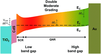
Graded band gap chalcopyrite solar cells are fabricated based on an all solution processable synthesis method with the aid of electrophoretic deposition and a superstrate structure. The solvothermally synthesized nanoparticles crystallize in the chalcopyrite–wurtzite mixed phase without any trace of impurity phases, as confirmed by XRD and Raman spectroscopy. Crack-free electrophoretic deposited films are formed. However, the porosity of the films is raised due to the Ga content. The JV characteristics of the CuIn1−xGaxS2 samples are compared with those of back extreme grading (BEG), back moderate grading (BMG), and double moderate grading (DMG) solar cells. The highest efficiency (JSC = 16.50 mA cm−2, VOC = 640 mV, fill factor = 0.61, η = 6.44%) is achieved in DMG cells, mainly due to reducing the minority carrier recombination at the absorber/back contact interface by back grading and increasing the photoresponse or open circuit voltage by front grading in the space charge region. The medium double grading in this structure avoids notch formation in the band structure. Dark diode analysis demonstrates that the lowest series resistance, shunt conductance and reverse saturation current are obtained, as well as a diode ideality factor near 2, in DMG solar cells.


1. Introduction

Lack of fossil fuel resources, air pollution, global warming, and population growth lead to the necessity of finding new energy resources. Renewable energies, especially solar energy, have the potential to fulfill the 21st century’s energy desires. Among all photovoltaic technologies, chalcopyrite solar cells with the advantages of having a direct and tunable band gap (1.04–2.5 eV), high absorption coefficient (>104 cm−1), appreciable record efficiency (19.9%), and respectable efficiency to cost ratio, introduce themselves as a promising technology to fulfill humankind’s future energy desires.1–3 However, the difficulties in fabricating large area modules, rarity of raw materials, need of costly high vacuum apparatus, and requirement for toxic post selenization treatments, limit the large scale production of these cells.4,5

The solution processable deposition of Cu(In1−xGax)(SySe1−y)2 (CIGS) compounds for the fabrication of solar cells attracts a great deal of attention due to its cost effectiveness, high production rate, ability for roll-to-roll production, compositional uniformity over large areas, and low material waste.6,7 A variety of solution processed methods have been utilized for the deposition of CIGS including spray pyrolysis,8 electrodeposition,9 spin coating,10 doctor blading,11 inkjet printing,12 and electrophoretic deposition (EPD).13 EPD is a low cost, simple, fast, and low waste method with the potential for the automation and the deposition of large area films.14 Although the ability of doctor blading for mass production is higher than EPD, this method always suffers from organic residues used to prepare the paste. EPD has been used for the deposition of quantum dots (QDs) in the fabrication processes for quantum dot sensitized solar cells (QDSCs). CdSe QDs were deposited using EPD to reach an efficiency of 1.48% in QDSCs.15 Kamat et al. used EPD to deposit CIGS quantum dots for the fabrication of a QDSC with an efficiency of 3.91%.16 However, the EPD of chalcopyrite compounds for the deposition of a thick absorber layer in solution processable solar cells has rarely been reported. A Cu2ZnSnS4 semiconductor was deposited via EPD to achieve a 500 nm thick film for application as an absorber layer.17

Since the band gap of chalcopyrite compounds can be tuned by changing the Ga/(In + Ga) and S/(Se + S) ratio in the range of 1.04–1.68 eV and 1.04–1.53 eV,18 respectively, different semiconductors with a slight lattice mismatch and difference in composition can be simply deposited. This composition dependent band gap allows for band gap grading strategies (including front, back, and double gradings) in order to fabricate a device with a tandem structure and surpass the Shockley–Queisser thermodynamic limit for a single planar junction solar cell or to reduce the recombination at the back contact by repelling minority carriers from the interface.19 In most cases, improved efficiencies are reported.20–23 In this article, all solution processable band gap graded CuIn1−xGaxS2 inverted type (superstrate) solar cells were fabricated and the effect of the tandem structure on the cell efficiency of these devices is investigated. Fabrication of these kinds of cells may pave the way to achieve flexible low cost solar cells.

2. Experimental

2.1 Materials

Copper chloride (CuCl2, ≥98%, Merck), indium chloride (InCl3, 99.99%, Alfa Aesar), sulfur powder (S, 99%, Merck), gallium nitrate (Ga(NO3)3, 98%, Merck), absolute ethanol (EtOH, Merck, 99%), 1-propanol (1-PrOH, 99.9%, Merck), deionized water (DIW, 18.2 MΩ), hydrochloric acid (HCl, 32%, Merck), tetrapropyl ortotitanate (TTiP, 98.5%, Merck), cadmium sulfate (3CdSO4·8H2O, 99.5%, Merck), thiourea (NH2–CS–NH2, 99%, Merck), ammonia (NH4OH, 30%, Merck), triethylenetetramine (TETA, 95%, Merck), and a fluorine doped tin oxide transparent conductive substrate (FTO, 15 Ω sq−1, Dyesol) were purchased and used as received.

2.2 TiO2 blocking layer deposition

The sol preparation method for depositing the blocking layer was reported elsewhere.24 Typically, TTiP was dissolved in 1PrOH for 10 min. In another beaker, a solution of 1PrOH, DIW, and HCl was prepared and added drop-wise to the former solution under vigorous stirring and stirred for 1 h. The blocking layer was deposited by dip coating of the prepared sol on pre-cleaned FTO substrates and dried at 100 °C for 10 min. The dip coating and drying processes were repeated twice to reach the thickness of about 100 nm. Then, the film was calcined at 450 °C for 1 h.

2.3 CdS window layer deposition

The CdS n-type layer was deposited through chemical bath deposition as reported elsewhere.25 For this purpose, 0.015 M CdSO4 in 2 ml DIW, 1.5 M thiourea in 1 ml DIW, and 2.6 ml NH4OH in 15 ml DIW solutions were separately prepared and added together before deposition. The substrates were placed in the bath at 80 °C for 12 min. The pale orange CdS deposited substrates were washed and dried.

2.4 CIGS electrophoretic deposition and device fabrication

CuIn1−xGaxS2 nanoparticles were synthesized via a modified solvothermal method according to a previous report.26 Briefly, stoichiometric amounts of CuCl2 (0.2 mmol), InCl3 (0–0.2 mmol), S (0.4 mmol), and Ga(NO3)3 (0–0.2 mmol) were placed into a homemade autoclave in triethylenetetramine as a solvent. The synthesis parameters of 220 °C for 1 h under an internal pressure of 400 kPa and continuous stirring were applied to the samples during the synthesis. Then, the autoclave was allowed to cool naturally to ambient temperature. The precipitates were collected by centrifugation and washing several times with ethanol to remove the organic residues and were then dried at 60 °C for 20 min.

Electrophoretic deposition of the nanoparticles was conducted according to a previous report with slight modification.27 For the electrophoretic deposition, the CuIn1−xGaxS2 nanoparticles were dispersed in EtOH (0.09% wt) by 30 min ultrasonication. A very small amount of TETA (4% vol.) was added to the colloid to increase the dispersibility and deposition current density of the nanoparticles. A DC current with constant voltage and FTO as the anode and TiO2/CdS coated FTO as the cathode were utilized. The electrophoretic deposition parameters were set to 60 V for 60 min with 0.3 cm as the distance between the anode and cathode. For the deposition of the back extreme grading cell (BEG), the colloids of CuInS2, CuIn0.75Ga0.25S2, CuIn0.5Ga0.5S2, CuIn0.25Ga0.75S2, and CuGaS2 were sequentially deposited by applying 60 V for 12 min for each colloid. The colloids of CuInS2, CuIn0.75Ga0.25S2, and CuIn0.5Ga0.5S2 were also successively applied by 60 V for 20 min for each colloid, for the deposition of the back moderate grading cell (BMG). Finally, the colloids of CuIn0.75Ga0.25S2, CuInS2, CuIn0.75Ga0.25S2, and CuIn0.5Ga0.5S2 were consecutively deposited by applying 60 V for 15 min for each colloid for the fabrication of the double moderate grading cell (DMG). After deposition, the films were washed by dipping in EtOH and dried naturally. The films were annealed at 250 °C for 30 min in air and at 400 °C for 1 h under an argon/H2S atmosphere. Finally, the Au layer with a thickness of about 500 nm was deposited on the film using magnetron sputtering through a shadow mask. The schematic structure and FESEM cross section of the CuIn0.5Ga0.5S2 device are shown in Fig. 1.


image file: c5ra26315h-f1.tif
Fig. 1 (a) Schematic representation of the tandem CIGS graded superstrate structure and (b) FESEM cross-sectional view of the electrophoretic deposited layers before Au deposition.

2.5 Characterization of the thin films and solar cells

The phase structure of the films was studied using X-ray diffraction (XRD), on a Philips X-pert pro PW1730, and using Cu-Kα radiation. Field emission scanning electron microscopy (FESEM), on a Hitachi S4160, was used to investigate the morphology of the films. Raman spectra were recorded using a BRUKER (SETERRA, spectral resolution < 3 cm−1) MicroRaman spectrometer (785 nm argon laser, 25 mW) equipped with a confocal microscope. Photovoltaic measurements were performed using an AM 1.5 solar simulator (Sharif Solar). The power of the simulated light was calibrated to 1000 W m−2 with a Si photodiode. JV curves were obtained by applying an external bias to the cell and measuring the generated photocurrent with a PGSTAT digital source meter. All tests were conducted at room temperature. Two cells with the same conditions for each parameter were fabricated for a repeatability test. Diffuse reflectance spectroscopy (DRS), on an Avalight DH-S Avaspec 2048 TEC, was performed to investigate the absorption coefficients and band gaps of the CIGS samples. The spectra were calibrated using the Kubelka–Munk function: F(R) = (1 − R2)/2R, where F(R) and R are the equivalent absorption coefficient and the reflectance, respectively.

3. Results and discussion

Fig. 2(a) shows the XRD patterns of the CuIn1−xGaxS2 nanoparticles synthesized using a solvothermal method. All samples crystallize in both the chalcopyrite and wurtzite crystal structures (JCPDS card no. 27-0159, 47-1372, and 25-0279).28,29 Although the chalcopyrite phase is thermodynamically more stable, the wurtzite metastable phase can be formed in CIGS nanoparticles with the assistance of the coordinating ligands, sulfur source type, coordinating solvent, sequence of metal reactions, reaction temperature, and concentration.30 The smaller size of the gallium ion compared to indium in the lattice causes a shift toward a higher diffraction angle with increasing gallium content. It is believed that the formation of the intermediate Cu2S phase is necessary for wurtzite formation.31,32 TETA can strongly bind to the In3+ cations and act as a ligand, manipulating the kinetics of wurtzite growth. The flexibility of the stoichiometry caused by the random distribution of ions in the wurtzite phase, provides the ability to tune the Fermi energy over a wide range, which is remarkably advantageous for photovoltaic applications.
image file: c5ra26315h-f2.tif
Fig. 2 (a) XRD patterns and (b) Raman spectra of the CuIn1−xGaxS2 nanoparticles.

The Raman spectra of the CuIn1−xGaxS2 nanoparticles are demonstrated in Fig. 2(b). The chalcopyrite semiconductors in the space group of D122d contain two formulae per primitive unit cell. The A1 TO modes are the strongest Raman modes at around 293 cm−1 for CuInS2 and 302 cm−1 for CuGaS2, which match well with the Raman spectrum of chalcopyrite compounds.33 The shoulder at around 302 cm−1 in the CuInS2 sample shows Cu–Au ordering (A*). The wurtzite CIGS phase shows four bands at 256, 288, 302 and 344 cm−1.34 These bands could be observed in the samples. However, they cannot be thoroughly separated from the chalcopyrite Raman modes. The CuxS compounds vibrate at 474 cm−1, and could not be detected in these samples, revealing the nonexistence of impurity phases.35

The FESEM images of CuIn1−xGaxS2 films are represented in Fig. 3. The particle size does not dramatically change with Ga content. However, larger agglomerates could be observed in Ga doped samples. Although relatively homogenous crack-free films are formed in all samples, the porosity of the films is affected by the Ga substitution. Large agglomerates in Ga doped samples cause large porosity in those films. The EDX analyses, and R1 = Cu/In + Ga, R2 = Ga/In + Ga, and R3 = S/Cu + In + Ga ratios of the CuIn1−xGaxS2 samples are tabulated in Table 1. The EDX analyses are well matched with the stoichiometry of the chalcopyrite compounds. The R1, R2, and R3 ratios show the occurrence of a slight off-stoichiometry in the samples, which is associated with the chemical synthesis route.


image file: c5ra26315h-f3.tif
Fig. 3 FESEM images of the CuIn1−xGaxS2 films with x equal to (a) 0, (b) 0.25, (c) 0.5, (d) 0.75 and (e) 1, and (f) graded CIS to CGS.
Table 1 EDX analyses, and R1 = Cu/In + Ga, R2 = Ga/In + Ga, and R3 = S/Cu + In + Ga ratios of the CuIn1−xGaxS2 samples
Sample Cu (at%) In (at%) Ga (at%) S (at%) R1 R2 R3
x = 0 29.20 23.28 0.00 47.53 1.25 0.00 0.91
x = 0.25 25.27 19.20 7.30 48.21 0.95 0.28 0.93
x = 0.5 25.62 13.58 15.53 45.26 0.88 0.53 0.83
x = 0.75 31.20 7.92 13.58 47.28 1.45 0.63 0.90
x = 1 26.33 0.00 29.72 43.94 0.89 1.00 0.78


Fig. 4 reveals the EDX line scans of BEG, BMG, and DMG CIGS thin film cross sections. The In/In + Ga content is gradually increased with distance from the back contact in BEG cells. The Cu and S content does not dramatically change in the different layers of the graded cell. In the case of BMG cells, the Ga content increases with distance from the back contact but with a lower slope. In the DMG sample, the layer deposition starts with CuIn0.5Ga0.5S2 through CuInS2 and ends with CuIn0.75Ga0.25S2.


image file: c5ra26315h-f4.tif
Fig. 4 EDX line scans of graded CuInxGa1−xS2: (a) BEG, (b) BMG, and (c) DMG CIGS thin film cross section.

Fig. 5(a) displays the DRS spectra of the CuInxGa1−xS2 solvothermally synthesized samples. The band gaps of the CuInxGa1−xS2 nanoparticles increase with increasing Ga content as expected. The band gap values of about 1.43, 1.56, 1.77, 1.96 and 2.29 eV could be calculated for x = 0, 0.25, 0.5, 0.75, and 1, respectively. The slightly lower band gaps of the CIGS nanoparticles in this research compared to other reported values may be attributed to the formation of InCu, GaCu, CuIn, and CuGa antisite defects.36 These defects cause a change of up to 0.29 eV in the band edge positions. The InCu2+ + 2VCu defect clusters are also very common in CIGS compounds, which can affect the band gap. However, the formation energies of VS, VCu, VIn, and Cui vacancies and interstitial defects are higher and less likely to occur. The band gap of CuIn1−xGaxS2 compounds can be well approximated by:

 
Eg(x) = xEg(1) + (1 − x)Eg(0) − b(1 − x)x (1)
where b is the bowing parameter and is the consequence of bond alternation in the lattice. The minimization of the free energy causes Cu and In atoms to avoid each other as nearest neighbors in the cation sublattice, resulting in short range ordering. b values of nearly 0 to 0.25 have been previously reported for CIGS.2 The b value of the nanoparticles is about 0.4, which is higher than the expected value and may be due to the wet chemical synthesis method. Fig. 5(b) shows that the color of the colloidal CIGS nanoparticles changes from dark brown to light brown with increasing Ga content.


image file: c5ra26315h-f5.tif
Fig. 5 (a) DRS spectra and (b) colloidal dispersion of the CuIn1−xGaxS2 nanoparticles.

The JV characteristic curves of the CuIn1−xGaxS2, BEG, BMG and DMG solar cells are exhibited in Fig. 6. The values of the short circuit current density (JSC), open voltage (VOC), fill factor (FF), and efficiency (η) of the cells are also listed in Table 2. The highest efficiency in the CuIn1−xGaxS2 samples is achieved when x = 0.25. The band gap of CuIn1−xGaxS2 semiconductors increases with Ga content mainly as a result of conduction band (CB) elevation. Shifting of the CB in the space charge region (SCR) causes an increase in VOC. However, the JSC is slightly decreased due to the lower absorption spectral region. Moreover, Ga widens the existence of the α-phase (the main chalcopyrite compound with an exact stoichiometry in the In2S3–Cu2S phase diagram) and consequently the tolerance to deviation from the Cu/In + Ga ratio. In addition, the c/a lattice constant ratio equals 2 when x ∼ 0.25, which reduces the defect concentration in this sample. The efficiency gradually drops in compounds with higher Ga content. Not only is there a slight increase in VOC and a dramatic decrease in JSC, but there is also a reduction in crystallinity and a more porous film is formed in compounds with higher Ga content, which causes this drop in efficiency. Besides, the lattice mismatch of the CGS film with the back contact is higher than that of the CIS film. Thus, it induces more recombination centers at the back contact. Also, since Ga evaporates more easily than In, it can lead to more 2VCu–GaCu+ defect clusters during the post treatment procedure, which enormously causes interface recombination centers. The FF of 61% is among the highest reported FFs for solution processed superstrate solar cells.37–39


image file: c5ra26315h-f6.tif
Fig. 6 JV characteristic curves of (a) the CuIn1−xGaxS2 solar cells and (b) BEG, BMG and DMG solar cells under dark and illuminated conditions.
Table 2 JV characteristic parameters of CuIn1−xGaxS2, BEG, BMG and DMG solar cells
Sample JSC (mA cm−2) VOC (mV) FF Eff. (%)
x = 0 14.50 580 0.60 5.05
x = 0.25 13.80 630 0.61 5.30
x = 0.5 10.60 670 0.59 4.19
x = 0.75 8.20 720 0.58 3.42
x = 1 6.50 755 0.56 2.75
BEG 10.30 560 0.45 2.60
BMG 15.80 585 0.60 5.55
DMG 16.50 640 0.61 6.44


Schematic representations of the band alignment in BEG, BMG and DMG solar cells are shown in Fig. 7. Of the graded cells, DMG cells show the highest efficiency compared to BMG, BEG and ungraded cells. On the other hand, BEG cells show the lowest efficiency among all cells, while their modified version, BMG cells, exhibit a high enough efficiency of 5.54%. Back grading can potentially increase the performance of the device by repelling CB minority carriers and reducing recombination at the back contact/absorber interface.40 Nevertheless, in the case of too strong grading, this results in a notch behind the SCR and increases the probability of charge recombination at the quasi neutral region.41 Therefore, the efficiency in BEG cells is unexpectedly lower. Moreover, the FF of this device is reduced due to extreme grading. Front grading cannot help to increase the device efficiency unless the grading is applied within the SCR. The concept of double grading (with front grading at the SCR and moderate back and front gradients) is found to be the most efficient grading configuration in CIGS solar cells.21,23 Since VOC mainly depends on the band gap in the SCR and JSC correlates to the overall minimum of the band gap, JSC can be improved due to a relatively higher spectral response and VOC can be optimized due to lower minority carrier recombination in DMG cells.


image file: c5ra26315h-f7.tif
Fig. 7 Schematic representation of the band alignment in BEG, BMG and DMG solar cells.

The diode curves in the dark for the BEG, BMG and DMG cells are demonstrated in Fig. 6(b). The diode curves can be analyzed using:

 
image file: c5ra26315h-t1.tif(2)
 
image file: c5ra26315h-t2.tif(3)
where jd, is the diode current density, j0 is the reverse saturation current density, e is the elementary electron charge, k is the Boltzmann constant, n is the diode ideality factor, RS is the series resistance, GSh is the shunt conductance, j00 is the pre-exponential factor, and Ea is the activation energy of the saturation current.42 A plot of dj/dV versus V gives GSh from the constant dj/dV when V ≤ 0. A plot of dV/dj versus 1/(jGShV) also estimates RS and n from the y intercept and slope in the high bias regime, respectively. A plot of ln(jGShV) versus VjRS gives j0 and n from the y intercept and slope, respectively. The values of RS, GSh, n, and j0 are calculated and show that the DMG device shows the lowest RS and GSh (25 Ω cm2 and 2.2 mS cm−2, respectively) values among all graded cells. The lower j0 value (1.5 × 10⁻³ mA cm−2) of DMG cells indicates less recombination in the SCR and the quasi neutral region (QNR) as a result of the double grading structure. An n equal to 1 corresponds to an ideal diode in which recombination occurs only in the QNR (with no recombination in the SCR). An n value close to 2 describes recombination in the SCR. An n value higher than 2 shows additional recombination mechanisms such as interface recombination and tunneling enhanced recombination.42 The n value of about 1.8 shows an appropriate diode ideality factor for this device.

Crossovers, kinks, or roll-overs could not be observed in the dark and illuminated curves of BMG and DMG solar cells, shown in Fig. 6(b). However, the curves obtained in the dark and under illumination of the BEG cells illustrate crossover. The crossover is due to the large electron barrier in the conduction band. Upon photodoping of the buffer layer, the potential drops over the buffer and thus the electron barrier is reduced. The high density of acceptors can also form the electron barrier. The large negative charge in the acceptor states leads to a large potential drop over the buffer layer. The absorber acceptors are filled under illumination and hence the acceptor charge and electron barrier are reduced.

4. Conclusions

All solution processable graded band gap chalcopyrite solar cells are fabricated for the first time using electrophoretic deposition and employing the superstrate structure of Au/CIGS(normal or graded)/CdS/TiO2/FTO. XRD and Raman spectroscopy confirm that the solvothermally synthesized nanoparticles crystallize in the chalcopyrite–wurtzite mixed phase without any trace of impurity phases. The crack-free films are formed using electrophoretic deposition, possessing different Ga content and using the three different grading strategies of BEG, BMG and DMG. The JV characteristics of the CuIn1−xGaxS2 samples are compared with those of BEG, BMG and DMG solar cells. The highest efficiency of 6.44% is achieved in DMG cells with JSC, VOC and FF of about 16.50 mA cm−2, 640 mV and 0.61, respectively. The main reasons for obtaining the highest improved efficiency in DMG cells are reducing the minority carrier recombination at the absorber/back contact interface by back grading, increasing the photoresponse or VOC by front grading in the SCR, and avoiding notch formation in the band structure by using a medium grading strategy. Lowest RS, GSh, J0, and n near 2 are obtained in DMG solar cell, which exhibit low recombination, appropriate interface quality, and high carrier life time in this cell.

Acknowledgements

We wish to thank The Iran National Science Foundation for supporting this research. The Iran Nanotechnology Initiative Council is gratefully acknowledged for partially supporting this research.

Notes and references

  1. D. Aldakov, A. Lefrancois and P. Reiss, Ternary and Quaternary Metal Chalcogenide Nanocrystals: Synthesis, Properties and Applications, J. Mater. Chem. C, 2013, 1, 3756–3776 RSC .
  2. B. J. Stanbery, Copper Indium Selenides and Related Materials for Photovoltaic Devices, CRC Crit. Rev. Solid State Sci., 2002, 27, 73–117 CrossRef CAS .
  3. J. Kolny-Olesiak and H. Weller, Synthesis and Application of Colloidal CuInS2 Semiconductor Nanocrystals, ACS Appl. Mater. Interfaces, 2013, 5, 12221–12237 CAS .
  4. S. E. Habas, H. A. S. Platt, M. F. A. M. van Hest and D. S. Ginley, Low-Cost Inorganic Solar Cells: From Ink to Printed Device, Chem. Rev., 2010, 110, 6571–6594 CrossRef CAS PubMed .
  5. A. C. Arias, J. D. MacKenzie, I. McCulloch, J. Rivnay and A. Salleo, Materials and Applications for Large Area Electronics: Solution-Based Approaches, Chem. Rev., 2010, 110, 3–24 CrossRef CAS PubMed .
  6. M. Graetzel, R. A. J. Janssen, D. B. Mitzi and E. H. Sargent, Materials Interface Engineering for Solution-Processed Photovoltaics, Nature, 2012, 488, 304–312 CrossRef CAS PubMed .
  7. W. Liu, D. B. Mitzi, M. Yuan, A. J. Kellock, S. J. Chey and O. Gunawan, 12% Efficiency CuIn(Se,S)2 Photovoltaic Device Prepared Using a Hydrazine Solution Process, Chem. Mater., 2010, 22, 1010–1014 CrossRef CAS .
  8. M. Kaelin, D. Rudmann and A. N. Tiwari, Low Cost Processing of CIGS Thin Film Solar Cells. Sol, Energy, 2004, 77, 749–756 CAS .
  9. J. S. Wellings, A. P. Samantilleke, S. N. Heavens, P. Warren and I. M. Dharmadasa, Electrodeposition of CuInSe2 from Ethylene Glycol at 150 °C, Sol. Energy Mater. Sol. Cells, 2009, 93, 1518–1523 CrossRef CAS .
  10. D. B. Mitzi, M. Yuan, W. Liu, A. J. Kellock, S. J. Chey, L. Gignac and A. G. Schrott, Hydrazine-Based Deposition Route for Device-Quality CIGS Films, Thin Solid Films, 2009, 517, 2158–2162 CrossRef CAS .
  11. M. Kaelin, D. Rudmann, F. Kurdesau, H. Zogg, T. Meyer and A. N. Tiwari, Low-Cost CIGS Solar Cells by Paste Coating and Selenization, Thin Solid Films, 2005, 480, 486–490 CrossRef .
  12. W. Wang, Y.-W. Su and C. Chang, Inkjet Printed Chalcopyrite CuInxGa1−xSe2 Thin Film Solar Cells, Sol. Energy Mater. Sol. Cells, 2011, 95, 2616–2620 CrossRef CAS .
  13. W. Guo and B. Liu, Liquid-Phase Pulsed Laser Ablation and Electrophoretic Deposition for Chalcopyrite Thin-Film Solar Cell Application, ACS Appl. Mater. Interfaces, 2012, 4, 7036–7042 CAS .
  14. L. Besra and M. Liu, A review on Fundamentals and Applications of Electrophoretic Deposition (EPD), Prog. Mater. Sci., 2007, 52, 1–61 CrossRef CAS .
  15. M. R. Golobostanfard, H. Abdizadeh and S. Mohajerzadeh, Incorporation of Carbon Nanotubes in a Hierarchical Porous Photoanode of Tandem Quantum Dot Sensitized Solar Cells, Nanotechnology, 2014, 25, 345402 CrossRef PubMed .
  16. P. K. Santra, P. V. Nair, K. G. Thomas and P. V. Kamat, CuInS2-Sensitized Quantum Dot Solar Cell. Electrophoretic Deposition, Excited-State Dynamics, and Photovoltaic Performance, J. Phys. Chem. Lett., 2013, 4, 722–729 CrossRef CAS PubMed .
  17. K. Kornhuber, J. Kavalakkatt, X. Lin, A. Ennaoui and M. Ch, Lux-Steiner, In Situ Monitoring of Electrophoretic Deposition of Cu2ZnSnS4 Nanocrystals, RSC Adv., 2013, 3, 5845–5850 RSC .
  18. I. Aguilera, J. Vidal, P. Wahnon, L. Reining and S. Botti, First-Principles Study of the Band Structure and Optical Absorption of CuGaS2, Phys. Rev. B: Condens. Matter Mater. Phys., 2011, 84, 085145 CrossRef .
  19. M. Gloeckler and J. R. Sites, Band-gap Grading in Cu(In,Ga)Se2 Solar Cells, J. Phys. Chem. Solids, 2005, 66, 1891–1894 CrossRef CAS .
  20. D. B. Mitzi, M. Yuan, W. Liu, A. J. Kellock, S. J. Chey, V. Deline and A. G. Schrott, A High-Efficiency Solution-Deposited Thin-Film Photovoltaic Device, Adv. Mater., 2008, 20, 3657–3662 CrossRef CAS .
  21. T. Dullweber, O. Lundberg, J. Malmstrom, M. Bodegard, L. Stolt, U. Rau, H. W. Schock and J. H. Werner, Back Surface Band Gap Gradings in CuZnGaSe Solar Cells, Thin Solid Films, 2001, 387, 11–13 CrossRef CAS .
  22. S. H. Sohn, N. S. Han, Y. J. Park, S. M. Park, H. S. An, D.-W. Kim, B. K. Min and J. K. Song, Band Gap Grading and Photovoltaic Performance of Solution-Processed Cu(In,Ga)S2 Thin-Film Solar Cells, Phys. Chem. Chem. Phys., 2014, 16, 27112–27118 RSC .
  23. S. Schleussner, U. Zimmermann, T. Watjen, K. Leifer and M. Edoff, Effect of Gallium Grading in Cu(In,Ga)Se2 Solar-Cell Absorbers Produced by Multi-Stage Coevaporation, Sol. Energy Mater. Sol. Cells, 2011, 95, 721–726 CrossRef CAS .
  24. M. R. Golobostanfard and H. Abdizadeh, Comparing Incorporation of Carbon Nanotubes in Hierarchical Porous Photoanodes of Quantum Dot and Dye Sensitized Solar Cells, Ceram. Int., 2015, 41, 497–504 CrossRef CAS .
  25. M. A. Contreras, M. J. Romero, B. To, F. Hasoon, R. Noufi, S. Ward and K. Ramanathan, Optimization of CBD CdS Process in High-Efficiency Cu(In,Ga)Se2-Based Solar Cells, Thin Solid Films, 2002, 403, 204–211 CrossRef .
  26. A. Khanaki, H. Abdizadeh and M. R. Golobostanfard, Effects of Process Parameters on The Synthesis and Characterization of CuIn1−xGaxSe2 Nanopowders Produced by New Modified Solvothermal Method, Mater. Sci. Semicond. Process., 2013, 16, 1397–1404 CrossRef CAS .
  27. A. Khanaki, H. Abdizadeh and M. R. Golobostanfard, Electrophoretic Deposition of CuIn1−xGaxSe2 Thin Films Using Solvothermal Synthesized Nanoparticles for Solar Cell Application, J. Phys. Chem. C, 2015, 119, 23250–23258 CAS .
  28. Y. Qi, Q. Liu, K. Tang, Z. Liang, Z. Ren and X. Liu, Synthesis and Characterization of Nanostructured Wurtzite CuInS2: A New Cation Disordered Polymorph of CuInS2, J. Phys. Chem. C, 2009, 113, 3939–3944 CAS .
  29. B. Koo, R. N. Patel and B. A. Korgel, Wurtzite-Chalcopyrite Polytypism in CuInS2 Nanodisks, Chem. Mater., 2009, 21, 1962–1966 CrossRef CAS .
  30. Y.-H. A. Wang, X. Zhang, N. Bao, B. Lin and A. Gupta, Synthesis of Shape-Controlled Monodisperse Wurtzite CuInxGa1−xS2 Semiconductor Nanocrystals with Tunable Band Gap, J. Am. Chem. Soc., 2011, 133, 11072–11075 CrossRef CAS PubMed .
  31. A. D. P. Leach, L. G. Mast, E. A. Hernandez-Pagan and J. E. Macdonald, Phase Dependent Visible to Near-Infrared Photoluminescence of CuInS2 Nanocrystals, J. Mater. Chem. C, 2015, 3, 3258–3265 RSC .
  32. M. E. Norako and R. L. Brutchey, Synthesis of Metastable Wurtzite CuInSe2 Nanocrystals, Chem. Mater., 2010, 22, 1613–1615 CrossRef CAS .
  33. H. Matsushita, S. Endo and T. Irie, Raman-Scattering Properties of I-III-VI2 Group Chalcopyrite Semiconductors, Jpn. J. Appl. Phys., 1992, 31, 18 CrossRef CAS .
  34. M. Gusain, P. Kumar and R. Nagarajan, Wurtzite CuInS2: Solution Based One Pot Direct Synthesis and Its Doping Studies with Nonmagnetic Ga3+ and Magnetic Fe3+ Ions, RSC Adv., 2013, 3, 18863–18871 RSC .
  35. D. Papadimitriou, N. Esser and C. Xue, Structural Properties of Chalcopyrite Thin Films Studied by Raman Spectroscopy, Phys. Status Solidi B, 2005, 242, 2633–2643 CrossRef CAS .
  36. S. B. Zhang, S.-H. Wei, A. Zunger and H. Katayama-Yoshida, Defect Physics of The CuInSe2 Chalcopyrite Semiconductor, Phys. Rev. B: Condens. Matter Mater. Phys., 1998, 57, 9642–9656 CrossRef CAS .
  37. H. S. An, Y. Cho, S. J. Park, H. S. Jeon, Y. J. Hwang, D.-W. Kim and B. K. Min, Cocktails of Paste Coatings for Performance Enhancement of CuInGaS2 Thin-Film Solar Cells, ACS Appl. Mater. Interfaces, 2014, 6, 888–893 CAS .
  38. D. Lee and K. Yong, Superstrate CuInS2 Photovoltaics with Enhanced Performance Using a CdS/ZnO Nanorod Array, ACS Appl. Mater. Interfaces, 2012, 4, 6758–6765 CAS .
  39. T. Nakada, T. Kume, T. Mise and A. Kunioka, Superstrate-Type Cu(In,Ga)Se2 Thin Film Solar Cells with ZnO Buffer Layers, Jpn. J. Appl. Phys., 1998, 37, 499–501 Search PubMed .
  40. T. Dullweber, U. Rau, M. A. Contreras, R. Noufi and H.-W. Schock, Photogeneration and Carrier Recombination in Graded Gap Cu(In,Ga)Se2 Solar Cells, IEEE Electron Device Lett., 2000, 47, 2249–2254 CrossRef CAS .
  41. A. Chirila, S. Buecheler, F. Pianezzi, P. Bloesch, C. Gretener, A. R. Uhl, C. Fella, L. Kranz, J. Perrenoud, S. Seyrling, R. Verma, S. Nishiwaki, Y. E. Romanyuk, G. Bilger and A. N. Tiwari, Highly Efficient Cu(In,Ga)Se2 Solar Cells Grown on Flexible Polymer Films, Nat. Mater., 2011, 10, 857–861 CrossRef CAS PubMed .
  42. Y. S. Lim, H.-S. Kwon, J. Jeong, J. Y. Kim, H. Kim, M. J. Ko, U. Jeong and D.-K. Lee, Colloidal Solution-Processed CuInSe2 Solar Cells with Significantly Improved Efficiency up to 9% by Morphological Improvement, ACS Appl. Mater. Interfaces, 2014, 6, 259–267 CAS .

This journal is © The Royal Society of Chemistry 2016